


Abstract
This study investigates the formation and evolution of nitrogen-vacancy (NV) centers in nitrogen-doped CVD diamonds. The diamonds were grown via the microwave plasma-assisted chemical vapor deposition (MPACVD) method with different levels of nitrogen doping, then irradiated with helium and hydrogen ions at different energies and doses, followed by low-pressure, high-temperature (LPHT) annealing at 1300 °C and 1400 °C. The presence and intensity of NV0 and NV− centers were identified and tracked by photoluminescence spectroscopy after each step. The results showed that both helium and hydrogen irradiation could induce NV center formation, with variation in NV0/NV− charge states depending on the irradiation conditions. Helium-irradiated samples generally exhibited stronger NV− signatures; however, the hydrogen-irradiated sample 5N10 (3 MeV, 1 × 10¹³ ions/cm2) displayed the most pronounced NV− presence of all samples, highlighting the critical role of nitrogen content and irradiation parameters. Ion irradiation reduced internal hydrostatic stress in all samples—from up to +0.23 GPa (compressive) in N5 and down to −0.82 GPa (tensile) in N10—relaxing stress toward near-zero values while increasing the Raman FWHM from ~3.5 cm−1 to up to 6.7 cm−1, indicating lattice disorder. LPHT annealing at 1300–1400 °C significantly increased NV-related photoluminescence, indicating effective thermal activation of vacancy-nitrogen recombination. Complementary Raman and FTIR analyses were employed to assess stress and defect evolution. The methodology enabled a comprehensive evaluation of the effects of irradiation and annealing on diamond defect structures, providing relevant experimental data for the controlled engineering of NV centers for quantum technologies.
1. Introduction
The advancement of microwave plasma-assisted chemical vapor deposition (MPCVD) techniques constituted a major step forward in materials engineering, enabling the large-scale production of high-purity, single-crystal diamond layers. The development of this technology, including breakthroughs in heteroepitaxial growth for wafer-scale production, was initially driven by the need for materials with extreme properties for applications in optics, electronics, and thermal management, aiming to overcome the scalability and purity limitations of natural or high-pressure, high-temperature (HPHT) diamonds [1].
It was within the context of studying and refining these high-quality diamonds that nitrogen-vacancy (NV) centers, a specific type of crystal defect, gained prominence. Although identified as photoluminescent defects in the 1970s [2], their quantum potential remained unrealized for decades [3]. Breakthroughs in the early 2000s revealed the NV center’s unique spin properties, including its ground-state triplet and optical spin polarization capabilities at room temperature [4,5]. These discoveries laid the groundwork for subsequent applications in quantum sensing and information processing, with early demonstrations showing nanoscale magnetic field sensitivity [6,7].
The research on NV centers in CVD diamond has undergone significant advancements through systematic investigations of their formation mechanisms, spin properties, and optimization strategies for quantum applications. Early breakthroughs demonstrated the interdependence of NV- concentration, spin coherence time (T2), and charge-state stability by varying nitrogen flow during growth and optimizing electron-irradiation fluences, achieving remarkable T2 values ranging from 45.5 μs to 549 μs [8]. Subsequent innovations introduced novel fabrication techniques, including high-energy photon irradiation using Ar+ plasma sources, which enabled the creation of approximately 20,000 NV− centers within the diffraction-limited sample volume of a type-IIa CVD-grown diamond with an as-grown nitrogen concentration of ~0.6 ppm while maintaining excellent spin properties (T1 = 5 ms, T2 = 4 μs) for enhanced DC and AC magnetic field sensitivity [9]. Parallel developments in diamond growth technology yielded ultrapure CVD films through microwave-assisted systems with minimized nitrogen contamination, coupled with advanced implantation methods featuring in situ ultrahigh vacuum processes and hot implantation to prevent surface charging effects [10]. Breakthroughs in high-density NV ensemble creation achieved concentrations up to 8.5 × 1018 cm−3 through precise electron beam narrowing in transmission electron microscopy, enabling studies of NV-NV interactions crucial for many-body quantum physics [11]. Further refinements addressed material challenges by demonstrating that increased substrate misorientation angles reduce inhomogeneous stress distributions, thereby extending spin dephasing times (T2*) for improved DC magnetic sensitivity [12]. Fundamental insights emerged from first-principles calculations revealing hydrogen’s critical role in NV center formation through stable NVH complexes and their orientation-dependent alignment with surface C-H bonds, particularly favoring (111)-oriented CVD growth to eliminate orientation domains [13]. These collective advances—spanning materials synthesis, defect engineering, spin control, and fundamental understanding—have established CVD diamond as a versatile platform for quantum sensing, with optimized NV properties enabling unprecedented sensitivity in magnetometry applications. The introduction of ultrahigh vacuum (UHV) implantation techniques further refined the process, minimizing lattice damage while stabilizing the negatively charged NV− state essential for quantum applications [10,14].
Quantum computing applications witnessed major milestones through the demonstration of room-temperature qubit operation with coherence times exceeding 1 millisecond using dynamical decoupling techniques [10]. Integration with nanophotonic structures enhanced photon collection efficiency, enabling more robust quantum networks [6]. The realization of multi-qubit entanglement in NV ensembles represented a critical step toward scalable quantum processors [7], while microelectronic readout systems improved signal detection fidelity [15].
In sensing and metrology, researchers achieved remarkable progress by developing high-density NV ensembles with concentrations up to 1019 cm−3; however, these are typically accompanied by a spin bath of ~50 ppm P1 centers, resulting in T2 values of a few microseconds [16]. Compact, integrated sensor designs incorporated on-chip microwave and optical components, enabling portable magnetometry applications [17,18]. Multimodal sensing platforms emerged, capable of simultaneous magnetic field and temperature measurements with nanoscale resolution [19], while diamond-embedded microwave antennas improved measurement stability [20].
Recent years have seen NV center technology expand into biological domains, enabling label-free biomolecule detection and intracellular thermometry [21,22]. Real-time vector magnetometry achieved unprecedented sensitivity below pT/√Hz [23], and hybrid quantum systems combined NV centers with silicon vacancies for enhanced functionality [7]. The influence of phosphorus donors on NV center stability was elucidated through first-principles studies [24], while parallel measurement techniques improved scalability [25].
Despite these advances, challenges remain in achieving uniform NV integration across large-area diamond wafers and further extending coherence times through spin bath noise suppression [14]. Commercialization efforts continue to address cost barriers and standardization needs [17], with particular focus on applications in navigation, materials science, and medical diagnostics [26]. The field now stands at an exciting juncture, where fundamental research converges with practical applications, promising transformative impacts across quantum technologies and beyond.
Despite this heightened attention, the research and applications of diamond NV centers face several significant challenges that must be addressed to fully realize their potential for quantum technologies. A primary obstacle lies in achieving high-quality single-crystal diamond through growth methods like heteroepitaxy, which often struggles to maintain the necessary crystal integrity for quantum applications [27]. Decoherence caused by environmental noise remains a persistent issue, limiting NV center performance despite ongoing efforts to enhance coherence times through techniques like the previously mentioned dynamical decoupling [10]. Fundamental understanding of NV center physics, including their interactions with strain fields, still contains unresolved aspects that hinder technological advancement [28]. Practical implementation faces additional hurdles such as low success probability, stringent technical requirements, and high production costs, along with challenges in defect control, characterization, and fabrication techniques [29]. The need to reduce impurities and surrounding spins while controlling NV density, spatial localization, charge state, and orientation presents further complications [4]. Creating large numbers of coherently coupled yet individually addressable NV centers represents another significant challenge [30].
Looking toward future directions, researchers are working to develop scalable production methods through advances in CVD techniques and ion implantation for deterministic NV center generation [10]. The field is expanding to explore alternative diamond defects like group IV color centers that may offer superior properties for quantum photonics [31]. Integration with quantum networks for secure communication and computing is being actively pursued [32], alongside efforts to improve photon collection efficiencies and generate entanglement while maintaining coherent nuclear spin memory [27]. Materials science approaches aim to enhance NV center performance for quantum sensors, networks, simulators, and scalable quantum computers [29]. Novel methods using strain gradients for position encoding and magnetic gradients for individual manipulation are being developed to advance quantum information processing [30]. While the complexity of quantum systems may present unforeseen difficulties, these ongoing advancements in diamond growth techniques and defect engineering suggest a promising future for NV center applications in quantum technology.
The controlled introduction of defects in diamond through ion or electron irradiation is a critical technique for engineering optical and quantum defects, such as NV centers. Among the various ion species used, helium and hydrogen irradiation are prominent due to their distinct interactions with the diamond lattice. This analysis evaluates their relative efficiencies, structural effects, and suitability for defect engineering.
Helium ion implantation is highly effective in generating vacancies, producing approximately an order of magnitude more vacancies than hydrogen ions at comparable doses [33]. This makes helium particularly advantageous for applications requiring high defect densities. Notably, helium irradiation induces a variety of optical centers, with prominent photoluminescence emission lines at approximately 534 nm (HR1; reported in the range 534–536 nm in the literature) and 560 nm (HR2), as reported by Khomich et al. [33]. Post-implantation annealing further transforms these spectra, activating more than a dozen distinct optical centers. However, helium irradiation poses several challenges. At high doses, such as 1 × 10¹⁷ ions/cm2, helium implantation can cause severe lattice damage, leading to fluorescence quenching and amorphization, as observed by McCloskey et al. [34]. Additionally, helium induces rapid lattice swelling, which can result in dechanneling at low doses, impairing vacancy uniformity [35]. Furthermore, high-energy helium implantation can generate A-type color centers and carbon nanoclusters, altering the diamond’s optical properties [36]. Despite these drawbacks, helium remains valuable for applications requiring high vacancy densities, though precise control of implantation parameters is essential to mitigate damage.
Hydrogen irradiation offers a less destructive alternative, with several key advantages. Hydrogen ions induce 16% less implantation damage than helium at optimized doses. Due to their lower mass, hydrogen microbeams enable high spatial precision, making them preferable for applications requiring depth-resolved defect engineering [35]. However, hydrogen implantation is not without limitations. Hydrogen can cause surface blistering and graphitization, particularly at high fluences, which may degrade structural integrity. Moreover, hydrogen generates significantly fewer vacancies than helium, limiting its utility for high-density defect applications [33].
Other techniques, such as electron irradiation, can also produce NV centers but often lack the spatial control and vacancy density achievable with ion implantation, as highlighted by Santonocito et al. [37]. The efficiency of NV formation depends on the competition between different vacancy types, which varies with the irradiation method. This comparative study was undertaken to evaluate the distinct effects of helium and hydrogen ion irradiation on NV center formation in CVD diamond while also investigating the complementary effects of LPHT annealing on defect evolution in helium-irradiated samples.
In this context, several studies have specifically explored helium and hydrogen irradiation as practical tools for NV center engineering. Ngandeu Ngambou et al. demonstrated that moderate He+ ion doses (4–8 × 10¹² ions/cm2) optimize the conversion of substitutional nitrogen into NV centers near the diamond surface, while excessive doses degrade spin properties [38]. Berzins et al. showed that tripling a previously considered optimal He+ implantation dose increases NV− magnetic sensitivity by nearly 30%, though at the cost of additional lattice damage requiring higher annealing temperatures [39]. On the hydrogen side, Findler et al. used NV centers themselves as local nanosensors to detect NVH− complexes via double electron–electron resonance, showing that NVH densities can exceed NV− densities by an order of magnitude in nitrogen-doped CVD layers when hydrogen is incorporated during growth [40], while Glover et al. and Goss et al. established the atomic structure and thermal stability of the NVH and VNH complexes via EPR and first-principles calculations, respectively [41,42]. These works collectively indicate that helium and hydrogen play distinct and sometimes competing roles in vacancy generation and nitrogen passivation, motivating the direct comparative approach adopted in the present study.
2. Materials and Methods
2.1. Diamond Growth
Two independent MPCVD growth experiments were performed to synthesize single-crystal diamond plates, hereafter referred to as groups N5 and N10, with nominal gas-phase nitrogen concentrations of approximately 14.7 ppm and 29 ppm, respectively. Both experiments were carried out using <100>-oriented single-crystal diamond seeds prepared in-house by our research group, which has full capability for seed preparation.
Prior to growth, the seeds with dimensions of 7 × 7 × 0.3 mm3 underwent a sequential cleaning procedure. They were first immersed in an ultrasonic bath of aqua regia (HCl + HNO3 in a 3:1 ratio) for 40 min at room temperature. Subsequently, they were sonicated in acetone for 10 min, followed by isopropanol for 10 min, and finally in deionized water for 10 min. After cleaning, the seeds were positioned on the substrate holder, with nine seeds loaded per growth run.
Diamond films were grown under fixed conditions of 950 °C and 120 Torr, using a gas mixture of 10% CH4 in H2 (purity 99.995% for CH4 and 99.9999% for H2). Nitrogen doping was achieved by adding a mixture of 0.1% N2 in H2 to the feed gas at flow rates of 5 sccm for group N5 and 10 sccm for group N10. The corresponding average growth rates were approximately 15.2 µm/h for N5 and 17.9 µm/h for N10. Growth continued until the diamond layer reached a thickness greater than 2 mm, excluding the original seed thickness, after which the process was stopped.
Each grown crystal was then laser-cut to remove both the seed substrate and the surrounding polycrystalline diamond. To minimize variations typically caused by temperature inhomogeneities during multi-crystal CVD growth, one representative crystal from each group, i.e., specifically the sample that exhibited the least temperature variation during growth, was selected for further processing. Both major faces of these crystals were polished using a standard steel disk for diamond finishing, after which they were sectioned into two plates of approximately 1 mm thickness. The newly exposed laser-cut faces were subsequently polished. Each of the four resulting plates with dimensions of 7 × 7 × 1 mm3 was then divided into four equal pieces of approximately 3 × 3 × 1 mm3. Finally, all pieces were subjected to a second aqua regia cleaning to remove any residual metallic contamination from the polishing step before undergoing irradiation experiments.
2.2. Ion Irradiation
The helium and hydrogen implantations were carried out by Professor Johnny Ferraz Dias at the Ion Implantation Laboratory, Institute of Physics, Federal University of Rio Grande do Sul, using a Tandetron ion accelerator, High Voltage Engineering Europa B.V. (HVEE), Amersfoort, The Netherlands. According to the literature [33,43] and our own data obtained from SRIM (Stopping and Range of Ions in Matter simulations) [44], the implantation energies of 2 and 3 MeV and doses of 1 × 10¹³ and 1 × 10¹⁴ ions/cm2 were selected as they provide sufficient energy to achieve significant penetration into the diamond while maintaining a fluence low enough to prevent excessive radiation damage. Only a single implantation cycle was performed for each condition. The irradiation protocol was guided by SRIM simulations, which calculated ion penetration depths and straggling for both helium and hydrogen in diamond. A summary of the irradiation conditions is provided in Table 1.
Table 1.
Irradiation conditions for each sample.
2.3. Low-Pressure High-Temperature Annealing
Two samples, 1N5 and 1N10, underwent LPHT annealing to study defect evolution and enhanced NV center formation. Two temperature points, 1400 °C for 1N5 and 1300 °C for 1N10, were chosen based on the distinct nitrogen concentrations of the two groups. For the lower-nitrogen N5 sample, a higher annealing temperature of 1400 °C was selected to maximize vacancy mobility and NV formation efficiency in a nitrogen-limited environment. For the higher-nitrogen N10 sample, 1300 °C was chosen as a more conservative temperature to promote NV center formation while limiting secondary defect aggregation (e.g., H3 and N3 centers), which can compete with NV formation at elevated temperatures, particularly in nitrogen-rich matrices. Both temperatures were selected to remain below the reported threshold for NV center thermal degradation (~1500–1600 °C for nitrogen-co-implanted samples), while promoting sufficient vacancy mobility for NV center formation. The samples were exposed to these temperatures for 30 min.
Characterization was performed after each preparation step. Photoluminescence spectroscopy was performed using a Horiba Labram HR Evolution (Horiba France SAS, Villeneuve d’Ascq, France) under 100× objective magnification and 514 nm laser excitation at room temperature to map the presence of defects and NV centers. The Raman peak position was analyzed to evaluate internal stress and lattice crystalline quality, with a spatial resolution of ~5 µm in the focal plane and a waist length of a few micrometers. This analysis was complemented by FTIR spectroscopy performed with a PerkinElmer Frontier spectrometer in basic transmission mode for evaluation of nitrogen incorporation and other related defects.
3. Results
3.1. CVD Diamond Growth
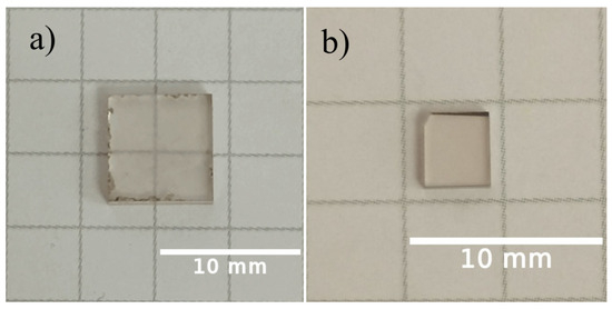
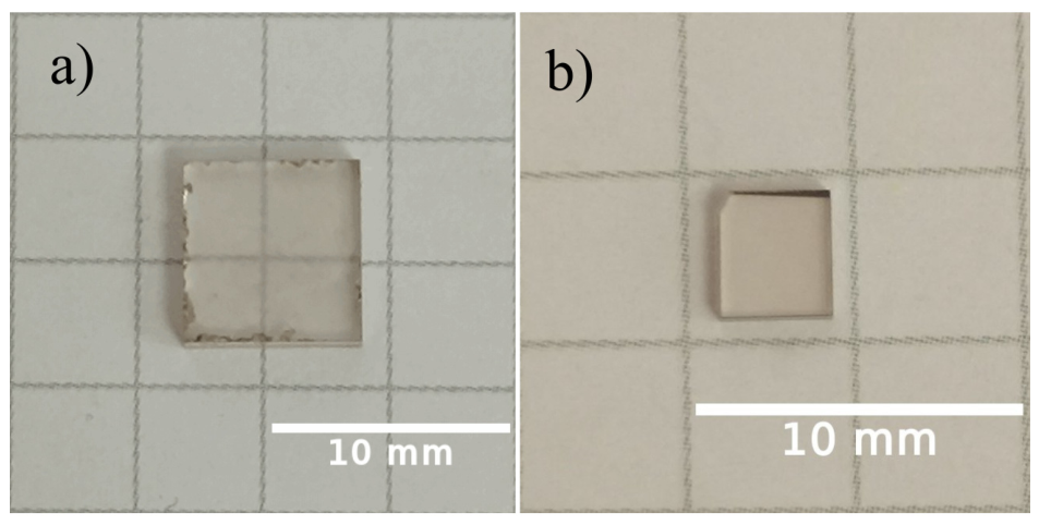
Figure 1 illustrates representative single-crystal diamonds grown via microwave plasma-assisted chemical vapor deposition (CVD) on silicon substrates, with average growth rates ranging from 15.6 for group N5 to 18.2 μm/h for group N10. Figure 1a shows an as-grown crystal from group N5, approximately 7 mm in side dimensions, after cleaning and laser removal of the polycrystalline rim. Figure 1b depicts one processed sample post-cutting and polishing, yielding a uniform, high-quality single-crystal platelet with flat facets and lateral dimensions of 3 mm. This refinement aims to minimize growth-induced inhomogeneities, ensuring uniform exposure of the samples to ion irradiation.
Figure 1.
Digital photographs of representative single-crystal CVD diamond samples from the nitrogen concentration group N5: (a) as-grown morphology, 7 × 7 × 2 mm3; (b) post-processing platelet 3 × 3 × 1 mm3 after laser excision of the seed substrate and polycrystalline edges and polishing.
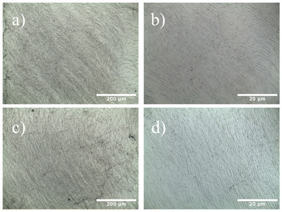
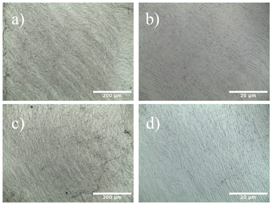
The optical microscopy images presented in Figure 2 for samples N5 and N10 before cutting and polishing reveal distinct surface morphologies characterized by visible growth steps, which vary in spacing and definition. Samples from group N5 (Figure 2a,b) exhibit broader and more widely spaced steps, whereas those from group N10 (Figure 2c,d) show a denser and more closely packed step pattern. This observation aligns with the expected evolution of step-flow growth morphology under increased nitrogen incorporation during CVD synthesis, as previously reported in our previous study [45] and others [46,47]. For instance, Achard et al. [47]. observed that at higher nitrogen concentrations (~75–200 ppm), macro-steps disappear as two-dimensional nucleation becomes more prominent, implying a reduction in the apparent size of the steps.
Figure 2.
Optical microscopy images of the as-grown sample surfaces. Images (a,b) show sample N5 at 10× and 100× magnification, respectively. Images (c,d) show sample N10, also at 10× and 100× magnification, respectively.
3.2. SRIM Simulations
The SRIM simulations summarized in Table 2 and Table 3 reveal key differences between helium and hydrogen ion irradiation in diamond within the 10 keV to 3 MeV energy range, which must be considered for defect and NV center engineering.
Table 2.
Helium irradiation in diamond.
Table 3.
Hydrogen irradiation in diamond.
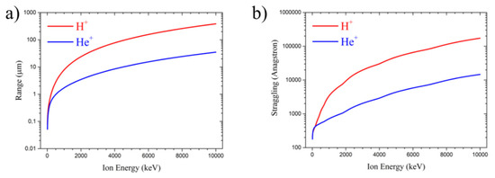
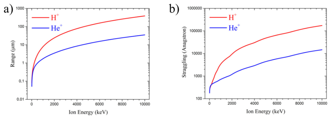
Figure 3a illustrates the ion implantation depth profiles in diamond. Hydrogen ions penetrate significantly deeper into the lattice than helium ions, making them more suitable for introducing defects in the bulk of the material. In contrast, helium ions deposit their energy closer to the surface, resulting in more localized damage. Helium also exhibits substantially higher nuclear stopping power than hydrogen, producing a greater number of lattice displacements per ion along its path. Although both ions show a reduction in stopping power with increasing energy, helium consistently generates more confined damage profiles. This contrast is further emphasized by the straggling behavior shown in Figure 3b, where hydrogen displays greater lateral and longitudinal straggling as a function of ion energy, leading to broader and more diffuse distributions of defects.
Figure 3.
Projected range (a) and straggling (b) as a function of ion implantation energy.
At 2 MeV, hydrogen ions have a projected range of approximately 24 μm in diamond, with broad straggling values (9.4 μm longitudinal and 7.7 μm lateral), enabling deep and diffuse defect formation throughout the bulk. In contrast, helium ions at the same energy penetrate only about 3.5 μm, with more confined damage (1.2 μm longitudinal and 1.1 μm lateral), favoring precise modification of near-surface regions. The nuclear stopping power of helium at this energy (0.041 eV/Å) remains significantly higher than that of hydrogen (0.0029 eV/Å). At 3 MeV, hydrogen ions reach approximately 47.5 μm in range with 19.7 μm longitudinal and 14.5 μm lateral straggling, whereas helium ions stop at around 5.8 μm with 2.04 μm longitudinal and 1.45 μm lateral straggling.
These intrinsic differences lead to distinct practical applications. Helium ion irradiation is more suitable for creating well-defined, defect-rich regions near the diamond surface, providing the spatial precision required for nanoscale devices and quantum sensing applications [33,39]. In contrast, hydrogen ions penetrate much deeper into the crystal, making them better suited for engineering bulk regions of diamond, as needed in volumetric quantum sensors or spin-based memory devices [43]. However, due to their lower stopping power, hydrogen ions typically require significantly higher fluences to achieve vacancy densities comparable to those generated by helium ions [33,43].
3.3. Photoluminescence Spectroscopy
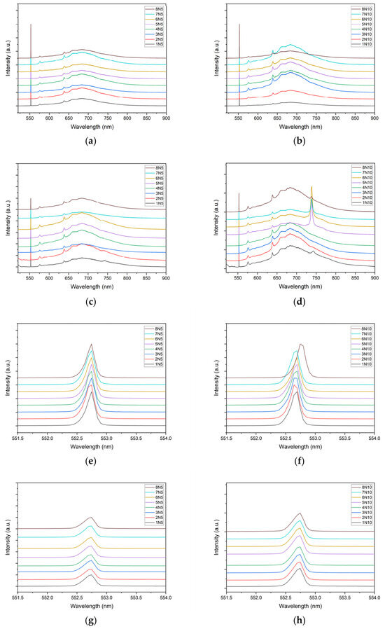
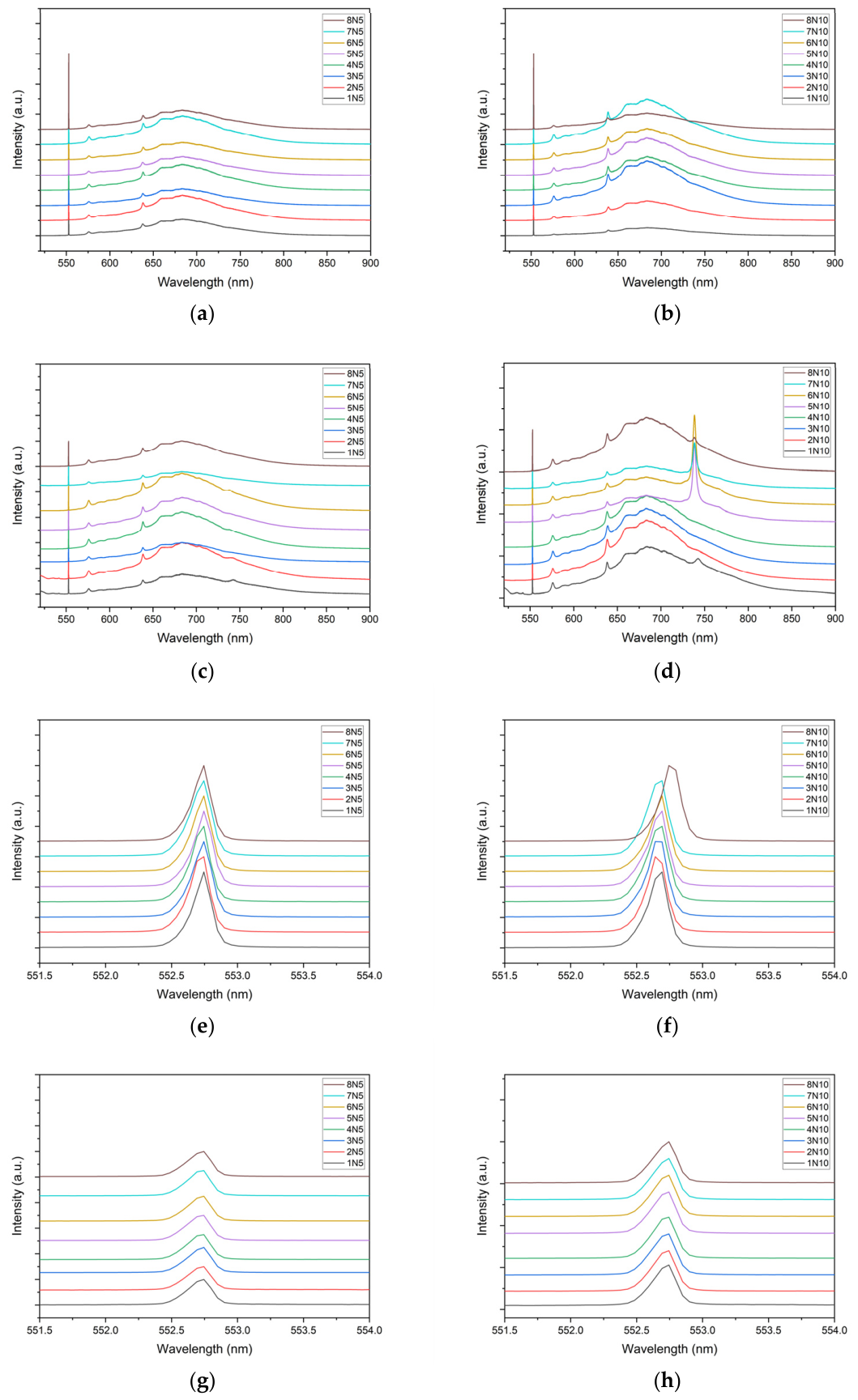
The photoluminescence spectra are presented in Figure 4, obtained under 514 nm laser excitation and normalized relative to the diamond characteristic peak at 552 nm. Distinct bands are observed at approximately 575 nm and 637 nm, corresponding to the neutral (NV0) and negatively charged (NV−) vacancy centers, respectively. These bands are followed by broad phonon sidebands, indicative of strong electron–phonon coupling. The spectral profiles vary among the samples, reflecting differences in NV0 and NV− center concentration, local strain, or formation conditions of each crystal. Overall, the spectral features confirm the dominance of NV-related luminescence, with minor peaks potentially attributed to other point defects, dislocations or stress-induced variations within the diamond lattice. The 534 nm and 542 nm emissions in the photoluminescence spectra were observed after irradiation for samples 1N10, 1N5 and 2N5 and are primarily associated with NV centers or the HR1 center in the case of the 534 nm band [33,48,49,50,51], and were suppressed after LPHT treatment.
Figure 4.
Photoluminescence spectra of all samples. The figure presents two distinct sample groups at different stages of preparation: (a) group N5 and (b) group N10 as-grown; (c) group N5 and (d) group N10 after the irradiation step. Within each irradiated panel, samples are identified by their ion species and conditions: samples 1N5, 2N5, 7N5, 8N5 (and their N10 counterparts) were irradiated with He ions (2 or 3 MeV; 1 × 10¹³ or 1 × 10¹⁴ ions/cm2); samples 3N5, 4N5, 5N5, 6N5 (and their N10 counterparts) were irradiated with H ions (2 or 3 MeV; 1 × 10¹³ or 1 × 10¹⁴ ions/cm2) (e–h) diamond Raman peak for each group. Full irradiation conditions for each sample are given in Table 1.
In the N5 group, photoluminescence data revealed that NV center formation varied depending on the ion type and energy. In helium-irradiated samples, such as 1N5 and 2N5, NV− centers were clearly dominant over NV0.
The hydrogen-irradiated samples in this group (3N5, 4N5, 5N5, and 6N5) showed more diverse behavior. Some, like 3N5, had relatively low NV-related emission intensities, while others, like 4N5 and 5N5, showed more intense signals—again with NV− being the dominant charge state. Sample 6N5 exhibited a more balanced distribution between NV0 and NV−, suggesting partial compensation. Interestingly, 7N5, which was also helium-irradiated (2 MeV, 1 × 10¹⁴ ions/cm2), had the weakest NV signals in the group, indicating less efficient center formation under those specific conditions. We note that only a single measurement was performed for each sample, so verification of reproducibility for sample 7N5 specifically, and for the dataset in general, is identified as a priority for future work.
Samples in the N10 group generally showed higher NV-related signal intensities compared to N5, particularly those irradiated with hydrogen. In the helium-irradiated subgroup (1N10, 2N10, 7N10, and 8N10), NV− remained the dominant species. Some samples, like 2N10, showed strong NV− signatures with relatively low NV0/NV− ratios, reinforcing the trend. Others, such as 1N10, showed a more balanced distribution, while some, like 7N10, exhibited low overall NV signal intensity, pointing to limited defect formation under the applied conditions.
Hydrogen-irradiated samples (3N10, 4N10, 5N10, and 6N10) displayed stronger and more evenly distributed NV signals. Sample 5N10 stood out with the most pronounced NV− presence, while 6N10 was notable for its near-equal proportions of NV0 and NV− center ZPL signals. These results suggest that higher fluences and energies of hydrogen ions favor the formation and stabilization of NV centers, while also promoting charge-state balance. A semi-quantitative evaluation of the NV−/NV0 charge-state ratio was performed by integrating the photoluminescence intensity within spectral windows centered on the zero-phonon lines at 637 nm (NV−) and 575 nm (NV0), including their respective phonon sidebands, after subtraction of the background luminescence. The resulting NV−/NV0 ratios are summarized in Table 4.
Table 4.
NV−/NV0 intensity ratio for all irradiated samples, calculated as the ratio between the total integrated photoluminescence areas of the NV− (637 nm) and NV0 (575 nm) charge states. Samples are grouped by nitrogen content series (N5 and N10).
Helium-irradiated samples in both groups (e.g., 1N5, 2N5, 1N10, 2N10) generally showed ratios above 1.5, consistent with NV− dominance. Among hydrogen-irradiated samples, 5N10 displayed the highest NV−/NV0 ratio in the entire dataset, underscoring that this apparent contradiction with the group-level trend is resolved when the dominant role of the N10 nitrogen concentration is considered: the higher nitrogen content of this group effectively stabilizes the NV− charge state even under hydrogen irradiation. These results emphasize that both ion species and nitrogen concentration jointly determine the charge-state distribution, and that group-level generalizations must account for this interaction. We note that a full, unambiguous quantification of NV−/NV0 ratios from PL spectra requires careful deconvolution of overlapping phonon sidebands and correction for relative quantum yields. Since these steps are beyond the scope of the present work, the reported values should be regarded as semi-quantitative, and a more detailed analysis will be addressed in future studies.
In addition, emission lines near 742 nm and 738 nm, which were not present in the as-grown samples, became detectable and even prominent in some samples after irradiation. Although these features are sometimes attributed in the literature to the neutral and the negatively charged silicon-vacancy centers: SiV0 and SiV−, respectively, the 742 nm line in this case is more reliably assigned to the GR1 center, which is associated with neutral vacancies in diamond and typically exhibits a zero-phonon line (ZPL) at 741 nm. The GR1 center forms readily under irradiation and is known to anneal out at high temperatures. This behavior is consistent with the observed disappearance of the 742 nm line after annealing at 1400 °C, strongly supporting its identification as GR1. In contrast, the negatively charged SiV− center, with its sharp and well-defined ZPL at 738 nm, is thermally stable up to at least 1400 °C and would not vanish under such conditions. While SiV0 can theoretically form via charge-state conversion of SiV− in nitrogen-rich diamonds due to irradiation-induced Fermi level shifts, its emission is rarely observed and difficult to isolate, especially given its spectral overlap with GR1. Therefore, in this case, the 742 nm emission is best explained by the presence of GR1 rather than SiV0 [52,53].
Although the NV center exhibits its characteristic ZPLs at 575 nm (NV0) and 637 nm (NV−), it may also contribute to secondary emissions near 542 nm through interactions with other lattice defects [54]. The N2V center, a more complex nitrogen-related defect consisting of two nitrogen atoms and a vacancy, is predominantly found in nitrogen-rich diamonds. While its primary emission lies in the near-infrared region, it can influence the overall photoluminescence spectrum in the visible range and may therefore be partially responsible for the observed emission near 542 nm [55]. Despite extensive investigations reported in the literature, the emission at 534 nm remains without a definitively established origin, although it has also been attributed to the HR1 center, as previously mentioned.
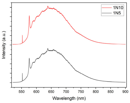
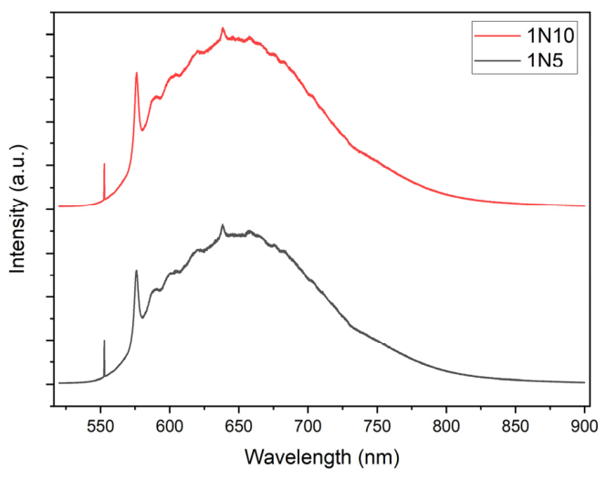
Figure 5 presents the photoluminescence spectra for samples 1N5 (black line in Figure 5) and 1N10 (red line in Figure 5), which showed similar behaviors after LPHT annealing treatment at 1400 °C and 1300 °C, respectively.
Figure 5.
Photoluminescence spectra of samples 1N5 and 1N10 after LPHT annealing.
Before the heat treatment, the samples showed relatively weak emissions, with the spectra dominated by background luminescence and less intense peaks in these regions. This is evidenced by comparing the photoluminescence spectra before and after the annealing process in the regions near 575 nm and 637 nm.
This behavior is typical for irradiated samples, where a large number of vacancies have been formed, but there has not yet been enough thermal mobilization for these vacancies to combine with substitutional nitrogen atoms (Ns) to form the NV0 and NV− centers. The thermal stability of NV defects is observed up to 1400 °C; at higher temperatures, they aggregate into complex defects like H3 and N3. In contrast, the aggregation temperature for these defects is considerably lower (1200 °C) in diamonds that have been heavily nitrogen-implanted and then high-pressure annealed. Diamonds co-implanted with nitrogen and helium demonstrate markedly enhanced thermal stability, with NV centers maintaining their intensity at temperatures up to 1600 °C [56,57,58].
After the annealing, a significant increase in emission intensity was observed. The NV center-related bands around 575 nm and 637 nm became more pronounced, with the NV− band becoming substantially more intense than the NV0 band. This behavior is consistent with what has been reported in the literature for irradiated CVD diamonds that have been subjected to heat treatments [57]. The reduction in background luminescence, especially above 700 nm, indicates the elimination of non-radiative defects and complex vacancy clusters that require the high energy provided by temperatures above 1300 °C to dissociate, improving vacancy mobility for NV formation [56,59].
The different responses between samples 1N5 and 1N10 can be attributed to variations in nitrogen content, the concentration of vacancies generated by irradiation, or the presence of residual defects that were not completely eliminated during the LPHT. Therefore, it is possible that sample 1N10 has a more favorable Ns concentration or a lower density of electron traps, resulting in a higher population of NV− after the heat treatment. The lack of new bands in the spectrum suggests that the formation of NV centers was the primary process activated by the LPHT treatment. This indicates that the growth and irradiation conditions were compatible with their selective and efficient formation.
3.4. Local Stress Analysis
The full width at half maximum (FWHM) of the diamond Raman peak was used as an indicator of crystalline integrity, and its position was used to estimate the local hydrostatic stress in a series of CVD diamond samples by analyzing the shift relative to the stress-free reference value at 1332 cm−1. The stress values were calculated using Equation (1):
where σ is the hydrostatic stress in GPa, Δshift = DRaman − 1332 is the shift in the measured Raman peak position DRaman in cm−1 relative to the unstressed diamond peak, and αh is the hydrostatic stress coefficient. In this study, a value of αh = 3 cm−1/GPa was adopted based on previous literature [60]. The results are compiled in Table 5.
Table 5.
Diamond Raman peak position, FWHM and respective stress calculations for each sample as grown and after the irradiation process.
Raman spectroscopy measurements revealed distinctions in internal stress and crystalline quality among the CVD diamond samples before and after ion irradiation. Non-irradiated samples in the group N5 exhibited positive values for Δshift, indicating mild compressive stress (up to +0.23 GPa), while those from group N10 showed significant negative shifts, corresponding to high tensile stress (down to −0.82 GPa). Upon irradiation with helium or hydrogen ions at doses ranging from 1 × 10¹³ to 1 × 10¹⁴ ions/cm2 and energies between 2 and 3 MeV, most samples exhibited a notable reduction in internal stress. In N5 samples, compressive stress was largely neutralized or even reversed to slight tension. In N10 samples, the initially high tensile stress was strongly reduced, with some cases reaching near-zero or even slightly compressive values. This stress relaxation, however, came at the cost of increased structural disorder, as evidenced by the broadening of the Raman peak. The increase was more pronounced in hydrogen-irradiated samples, particularly with 2 MeV ions, reaching FWHM values up to 6.7 cm−1, indicating significant lattice damage. Helium irradiation caused milder peak broadening, suggesting it is a more favorable option when aiming to control internal stress without severely compromising crystal quality. Overall, ion irradiation proved effective for tuning hydrostatic stress in CVD diamond, especially in nitrogen-rich films, though trade-offs in lattice integrity must be considered. A commercially available Element Six electronic-grade CVD diamond was also measured, showing an FWHM of 3.63 cm−1 and a Raman peak centered at 1331.79 cm−1. This reference was used both to validate the instrument’s resolution and Raman shift accuracy and to provide a benchmark of structural quality, reinforcing that the obtained structural integrity is still suitable for advanced applications.
Post-annealing Raman measurements for sample 1N10 exhibited a Raman peak at 1331.57 cm−1 with an FWHM of 5.785 cm−1, while sample 1N5 showed a peak at 1331.815 cm−1 and an FWHM of 5.543 cm−1. These values are comparable to their pre-annealed states, indicating that the irradiation-induced lattice defects responsible for FWHM broadening and stress relaxation are stable under these LPHT treatment conditions, and more intense thermal protocols or a longer annealing time may be necessary to restore pristine crystalline order without significantly harming NV center concentration. It is worth noting that previous work has demonstrated that while prolonged LPHT annealing can enhance optical properties of CVD diamond, treatment above 1400 °C risks promoting defect aggregation into H3 or N3 complexes [56]. Our 30 min protocol was deliberately chosen to balance NV formation efficiency against this risk, which explains the limited structural recovery observed in the Raman data.
3.5. Fourier Transform Infrared Spectroscopy
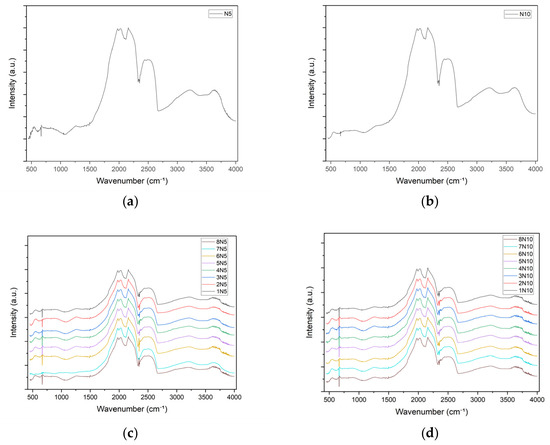
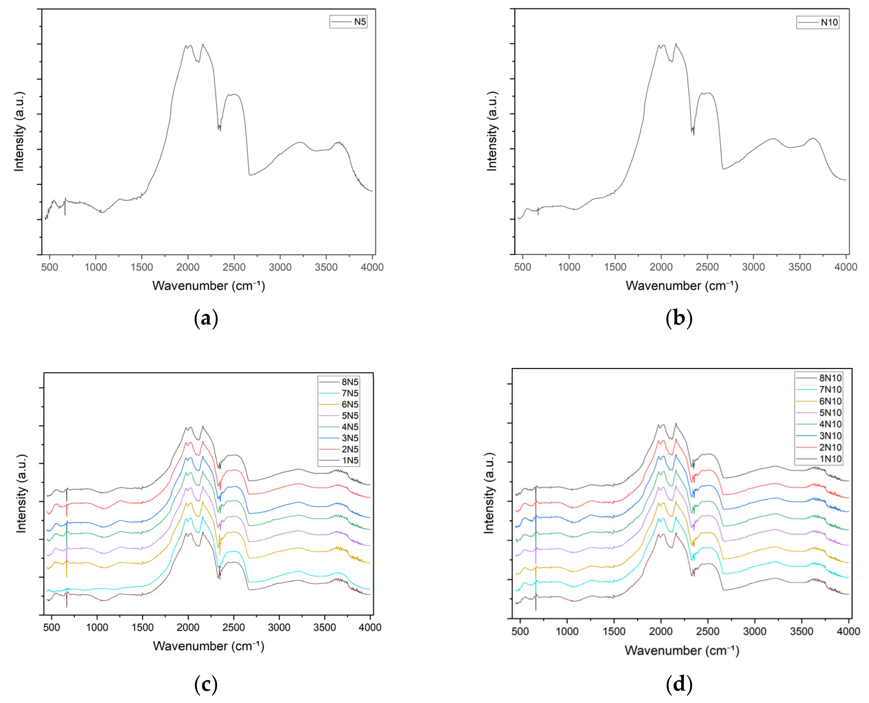
FTIR spectroscopy was carried out on samples before laser cutting for individual sample preparation and after the irradiation step to assess nitrogen incorporation into the diamond lattice and to investigate potential defects induced by ion bombardment. As shown in Figure 6, the spectrum displays the characteristic multiphonon absorption bands of diamond in the 1600–2600 cm−1 region. Additionally, very weak absorption features were observed around 2850 and 2920 cm−1, corresponding to C–H stretching vibrations; however, no evidence of hydrogen-related [61] electronic transitions was found.
Figure 6.
FTIR absorption spectra of the samples. Panels (a,b) show representative spectra of groups N5 and N10, respectively, in their as-grown state. Panels (c,d) display the full set of spectra for each group after irradiation: (c) for group N5 and (d) for group N10.
In an ideal diamond crystal, absorption in the one-phonon region is symmetry-forbidden; however, the presence of lattice defects can locally disturb this symmetry, enabling infrared activity in this range. In the present spectrum, a broad absorption band between 1000 and 1400 cm−1 was observed, which is likely linked to defect-related vibrational modes commonly reported in nitrogen-containing CVD diamonds [62,63]. Although distinct peaks such as those at 1046, 1130, 1332, 1353, and 1371 cm−1—e.g., reported by Wang et al. and Zaitsev et al. [64]—were not distinctly observed, the overall absorption pattern in this region suggests the influence of similar nitrogen-related defect structures. Similarities between N5 and N10 spectra indicate comparable defect profiles despite varying nitrogen levels.
The FTIR spectra of samples N5 and N10 (Figure 6a,b), acquired prior to laser cutting into individual pieces, exhibit features typical of nitrogen-doped CVD diamond, including a broad absorption band between 1000 and 1400 cm−1 in the one-phonon region, activated by local symmetry breaking associated with nitrogen-related defects. Notably, no distinct peak was observed at 3123 cm−1, the characteristic NVH0 stretching mode reported in the literature [41,42]. This absence indicates that, under the present irradiation conditions (2–3 MeV, 1 × 10¹³–1 × 10¹⁴ ions/cm2), hydrogen implantation did not produce a detectable population of NVH complexes, consistent with the comparatively low fluences employed relative to those in studies reporting NVH incorporation during CVD growth itself [40]. The overlaid spectra of the irradiated subsets (Figure 6c,d) show only minor variations in intensity and shape within the 1000–1400 cm−1 region, with no significant differences between the N5 and N10 groups despite their different nitrogen content. In the absence of a clear spectroscopic signature, we attribute these subtle variations to the general population of nitrogen-related point defects (Ns+, C-centers) rather than to NVH formation. We therefore conclude that, within the sensitivity of our FTIR measurements, hydrogen irradiation at the doses studied here did not generate a measurable concentration of NVH complexes.
4. Conclusions
This study investigated the formation and activation of NV centers in nitrogen-doped CVD diamond samples subjected to helium and hydrogen ion irradiation followed by LPHT annealing. Photoluminescence measurements confirmed the successful generation of NV0 and NV− centers under a range of irradiation conditions, with helium-irradiated samples generally showing stronger NV− signatures than hydrogen-irradiated ones when nitrogen content is held constant. However, the hydrogen-irradiated sample 5N10 exhibited the most pronounced NV− presence across the entire dataset, which is not a contradiction but rather reflects the decisive role of the higher nitrogen concentration of the N10 group in stabilizing the NV− charge state. This result underscores that both ion species and matrix nitrogen concentration jointly govern NV− formation efficiency. However, considerable variation was observed within each group, suggesting that local growth conditions and defect interactions significantly influence NV formation efficiency and charge-state distribution. LPHT annealing enhanced NV-related emissions in all treated samples, with the disappearance of GR1 and HR1 features indicating effective transformation of irradiation-induced vacancies into NV centers. FTIR spectra showed no clear evidence of NVH complex formation under the applied hydrogen irradiation conditions. Raman analysis revealed that ion implantation reduced internal stress, particularly in hydrogen-irradiated samples, but introduced measurable lattice disorder. These results demonstrate the viability of ion irradiation and annealing strategies for NV center engineering in CVD diamond while also highlighting the sensitivity of the outcome to growth parameters and irradiation protocols.
Author Contributions
Conceptualization, J.V.d.S.N., J.S.G. and V.J.T.-A.; methodology, J.V.d.S.N., J.S.G., J.F.D., A.M.Z., E.J.C. and V.J.T.-A.; investigation, J.V.d.S.N. and J.S.G.; formal analysis, J.V.d.S.N.; writing—original draft preparation, J.V.d.S.N.; writing—review and editing, all authors; supervision, E.J.C. and V.J.T.-A. All authors have read and agreed to the published version of the manuscript.
Funding
This research was funded by FAPESP and CNPq, grant 2023/02807-0, and FAPESP grant 2019/18572-7.
Data Availability Statement
The data supporting the findings of this study are available from the corresponding author upon reasonable request.
Acknowledgments
We especially thank the Ion Implantation Laboratory at UFRGS and Johnny F. Dias for their support and assistance with the ion implantation experiments and Alexander M. Zaitsev for his valuable guidance and support with the LPHT annealing treatments. During the preparation and revision of this manuscript, the authors used Claude Sonnet 5, developed by Anthropic, to improve the writing and clarity of the text and to assist in checking the consistency and numbering of in-text citations with the corresponding reference list. The authors have reviewed and edited the generated output and take full responsibility for the content of this publication.
Conflicts of Interest
Author José Vieira da Silva Neto was employed by the company TCarbon Diamond LTDA. The remaining authors declare that the research was conducted in the absence of any commercial or financial relationships that could be construed as a potential conflict of interest.
References
- Engels, J.; Weippert, J.; Luo, T.; Kustermann, J.; Quellmalz, P.; Mathes, N.; Lindner, L.; Giese, C.; Kirste, L.; Knittel, P. High ODMR contrast and alignment of NV centers in microstructures grown on heteroepitaxial diamonds. Appl. Phys. Lett. 2024, 124, 164001. [Google Scholar] [CrossRef] [Scilit]
- Davies, G.; Hamer, M.F. Optical studies of the 1.945 eV vibronic band in diamond. Proc. R. Soc. Lond. Ser. A Math. Phys. Sci. 1976, 348, 285–298. [Google Scholar] [CrossRef] [Scilit]
- Liu, Y.-C.; Dzeng, Y.-C.; Ting, C.-C. Nitrogen vacancy-centered diamond qubit: The fabrication, design, and application in quantum computing. IEEE Nanotechnol. Mag. 2022, 16, 37–43. [Google Scholar] [CrossRef] [Scilit]
- Achard, J.; Jacques, V.; Tallaire, A. Chemical vapour deposition diamond single crystals with nitrogen-vacancy centres: A review of material synthesis and technology for quantum sensing applications. J. Phys. D Appl. Phys. 2020, 53, 313001. [Google Scholar] [CrossRef] [Scilit]
- Takahashi, S.; Hanson, R.; van Tol, J.; Sherwin, M.S.; Awschalom, D.D. Quenching Spin Decoherence in Diamond through Spin Bath Polarization. Phys. Rev. Lett. 2008, 101, 47601. [Google Scholar] [CrossRef] [Scilit]
- Schröder, T.; Mouradian, S.L.; Zheng, J.; Trusheim, M.E.; Walsh, M.; Chen, E.H.; Li, L.; Bayn, I.; Englund, D. Quantum nanophotonics in diamond. J. Opt. Soc. Am. B 2016, 33, B65–B83. [Google Scholar] [CrossRef] [Scilit]
- Ramponi, R.; Coccia, G.; Guo, Y.; Kuriakose, A.; Alam, S.; Shahbazi, S.; Bennett, A.J.; Bharadwaj, V.; Hadden, J.P.; Jedrkiewicz, O. Diamond platform for Quantum Technologies: Laser and ion beam writing. In 2024 24th International Conference on Transparent Optical Networks (ICTON); IEEE: New York, NY, USA, 2024; p. 1. [Google Scholar]
- Luo, T.; Lindner, L.; Langer, J.; Cimalla, V.; Vidal, X.; Hahl, F.; Schreyvogel, C.; Onoda, S.; Ishii, S.; Ohshima, T. Creation of nitrogen-vacancy centers in chemical vapor deposition diamond for sensing applications. New J. Phys. 2022, 24, 033030. [Google Scholar] [CrossRef] [Scilit]
- Karki, P.B.; Timalsina, R.; Dowran, M.; Aregbesola, A.E.; Laraoui, A.; Ambal, K. An efficient method to create high-density nitrogen-vacancy centers in CVD diamond for sensing applications. Diam. Relat. Mater. 2023, 140, 110472. [Google Scholar] [CrossRef] [Scilit]
- Chakraborty, T.; Lehmann, F.; Zhang, J.; Borgsdorf, S.; Wöhrl, N.; Remfort, R.; Buck, V.; Köhler, U.; Suter, D. CVD growth of ultrapure diamond, generation of NV centers by ion implantation, and their spectroscopic characterization for quantum technological applications. Phys. Rev. Mater. 2019, 3, 065205. [Google Scholar] [CrossRef] [Scilit]
- Hayasaka, K.; Kanehisa, K.; Ueda, M.; Kimura, K.; Tanii, T.; Onoda, S.; Enomoto, S.; Kawarada, H. High-density NV Ensemble with Mutual Interaction of NV Centers Created in Ultra Heavily Nitrogen-doped CVD Diamond. Res. Sq. 2023. [Google Scholar] [CrossRef] [Scilit]
- Tsuji, T.; Sekiguchi, T.; Iwasaki, T.; Hatano, M. Extending Spin Dephasing Time of Perfectly Aligned Nitrogen-Vacancy Centers by Mitigating Stress Distribution on Highly Misoriented Chemical-Vapor-Deposition Diamond. Adv. Quantum Technol. 2024, 7, 2300194. [Google Scholar] [CrossRef] [Scilit]
- Feng, Y.; Li, X.-Z.; Wang, E.G.; Zhang, S.B.; Zhang, L. Microscopic origin for the orientation dependence of NV centers in chemical-vapor-deposited diamond. J. Phys. Condens. Matter 2014, 26, 485004. [Google Scholar] [CrossRef] [Scilit]
- Nebel, C.E. Nitrogen-vacancy doped CVD diamond for quantum applications: A review. Semicond. Semimet. 2020, 103, 73–136. [Google Scholar] [CrossRef] [Scilit]
- Wirtitsch, D.; Wachter, G.; Reisenbauer, S.; Schalko, J.; Schmid, U.; Fant, A.; Sant, L.; Trupke, M. Microelectronic readout of a diamond quantum sensor. arXiv 2024, arXiv:2403.03090. [Google Scholar]
- Bauch, E.; Singh, S.; Lee, J.; Hart, C.A.; Schloss, J.M.; Turner, M.J.; Barry, J.F.; Pham, L.M.; Bar-Gill, N.; Yelin, S.F.; et al. Decoherence of ensembles of nitrogen-vacancy centers in diamond. Phys. Rev. B 2020, 102, 134210. [Google Scholar] [CrossRef] [Scilit]
- Pogorzelski, J.; Horsthemke, L.; Homrighausen, J.; Stiegekötter, D.; Gregor, M.; Glösekötter, P. Compact and fully integrated led quantum sensor based on nv centers in diamond. Sensors 2024, 24, 743. [Google Scholar] [CrossRef] [Scilit]
- Zeng, S.; Yang, S.; Shang, Z.; He, X. NV color center fluorescence signal measurement based on FPGA architecture. J. Phys. Conf. Ser. 2024, 2740, 012008. [Google Scholar] [CrossRef] [Scilit]
- Zhu, X.; Wu, H.; Chen, B.; Yu, T.; Qian, P.; Fan, J.-W.; Chen, B. Joint quantum sensing of vector magnetic field and temperature with nitrogen-vacancy centers in diamond. Appl. Phys. Lett. 2023, 123, 244002. [Google Scholar] [CrossRef] [Scilit]
- Guo, Y.; Zhao, J.; Weng, C.; Lin, S.; Yang, Y.; Zhu, W.; Lou, L.; Wang, G. Robust diamond-embedded microwave antenna for optimizing quantum sensing using nitrogen-vacancy center ensembles. Appl. Phys. Lett. 2023, 123, 264003. [Google Scholar] [CrossRef] [Scilit]
- Zalieckas, J.; Greve, M.M.; Bellucci, L.; Sacco, G.; Håkonsen, V.; Tozzini, V.; Nifosì, R. Quantum sensing of microRNAs with nitrogen-vacancy centers in diamond. Commun. Chem. 2024, 7, 101. [Google Scholar] [CrossRef] [Scilit]
- Rizzato, R.; von Grafenstein, N.R.; Bucher, D.B. Quantum sensors in diamonds for magnetic resonance spectroscopy: Current applications and future prospects. Appl. Phys. Lett. 2023, 123, 260502. [Google Scholar] [CrossRef] [Scilit]
- Thooppanom, N.; Yodsungnoen, R.; Sapermsap, N.; Sangtawesin, S. Real Time Vector Magnetometry with Quantum Diamond Sensor. J. Phys. Conf. Ser. 2025, 2934, 012022. [Google Scholar] [CrossRef] [Scilit]
- Zou, D.; Shen, S.; Li, L.; Wang, Q.; Liang, K.; Chen, L.; Wu, G.; Shen, W. Influence of phosphorus donor on the NV center in diamond: A first-principles study. Phys. B Condens. Matter 2024, 676, 415614. [Google Scholar] [CrossRef] [Scilit]
- Cambria, M.; Chand, S.; Reiter, C.; Kolkowitz, S. Scalable parallel measurement of individual nitrogen-vacancy centers. arXiv 2024, arXiv:2408.11715. [Google Scholar]
- Hart, J.W.; Knowles, H.S. Multimodal quantum metrology in living systems using nitrogen-vacancy centres in diamond nanocrystals. Front. Quantum Sci. Technol. 2023, 2, 1220015. [Google Scholar] [CrossRef] [Scilit]
- Oshnik, N.O.; Westrich, S.; Burmeister, N.; Opaluch, O.; Mehmel, L.; Issaoui, R.; Tallaire, A.; Brinza, O.; Achard, J.; Neu-Ruffing, E. Nitrogen-Vacancy Centers in Epitaxial Laterally Overgrown Diamond: Towards Up-scaling of Color Center-based Quantum Technologies. Mater. Quantum Technol. 2025, 5, 025201. [Google Scholar] [CrossRef] [Scilit]
- Doherty, M.W.; Manson, N.B.; Delaney, P.; Jelezko, F.; Wrachtrup, J.; Hollenberg, L.C.L. The nitrogen-vacancy colour centre in diamond. Phys. Rep. 2013, 528, 1–45. [Google Scholar] [CrossRef] [Scilit]
- Rodgers, L.V.H.; Hughes, L.B.; Xie, M.; Maurer, P.C.; Kolkowitz, S.; Bleszynski Jayich, A.C.; de Leon, N.P. Materials challenges for quantum technologies based on color centers in diamond. MRS Bull. 2021, 46, 623–633. [Google Scholar] [CrossRef] [Scilit]
- Xu, Z.; Yin, Z.; Han, Q.; Li, T. Quantum information processing with closely-spaced diamond color centers in strain and magnetic fields. Opt. Mater. Express 2019, 9, 4654–4668. [Google Scholar] [CrossRef] [Scilit]
- Bradac, C.; Gao, W.; Forneris, J.; Trusheim, M.E.; Aharonovich, I. Quantum nanophotonics with group IV defects in diamond. Nat. Commun. 2019, 10, 5625. [Google Scholar] [CrossRef] [Scilit]
- Childress, L.; Hanson, R. Diamond NV centers for quantum computing and quantum networks. MRS Bull. 2013, 38, 134–138. [Google Scholar] [CrossRef] [Scilit]
- Khomich, A.A.; Popovich, A.; Khomich, A.V. Photoluminescence Spectra of Helium Ion-Implanted Diamond. Materials 2024, 17, 5168. [Google Scholar] [CrossRef] [Scilit]
- McCloskey, D.; Fox, D.; O’Hara, N.; Usov, V.; Scanlan, D.; McEvoy, N.; Duesberg, G.S.; Cross, G.L.W.; Zhang, H.Z.; Donegan, J.F. Helium ion microscope generated nitrogen-vacancy centres in type Ib diamond. Appl. Phys. Lett. 2014, 104, 031109. [Google Scholar] [CrossRef] [Scilit]
- Dooley, S.P.; Jamieson, D.N.; Prawer, S. He+ and H+ mubeam damage, swelling and annealing in diamond. Nucl. Instrum. Methods Phys. Res. B 1993, 77, 484–491. [Google Scholar] [CrossRef] [Scilit]
- Lopatin, O.N.; Nikolaev, A.G.; Valeev, V.F.; Nuzhdin, V.I.; Khaibullin, R.I. Crystal-Chemical Features of Diamonds Implanted with Helium Ions. Crystallogr. Rep. 2018, 63, 327–330. [Google Scholar] [CrossRef] [Scilit]
- Santonocito, S.; Denisenko, A.; Stöhr, R.; Knolle, W.; Schreck, M.; Markham, M.; Isoya, J.; Wrachtrup, J. NV centres by vacancies trapping in irradiated diamond: Experiments and modelling. New J. Phys. 2024, 26, 013054. [Google Scholar] [CrossRef] [Scilit]
- Ngandeu Ngambou, M.W.; Perrin, P.; Balasa, I.; Brinza, O.; Valentin, A.; Mille, V.; Bénédic, F.; Goldner, P.; Tallaire, A.; Achard, J. Optimizing ion implantation to create shallow NV centre ensembles in high-quality CVD diamond. Mater. Quantum Technol. 2022, 2, 045001. [Google Scholar] [CrossRef] [Scilit]
- Berzins, A.; Grube, H.; Sprugis, E.; Vaivars, G.; Fescenko, I. Impact of Helium Ion Implantation Dose and Annealing on Dense Near-Surface Layers of NV Centers. Nanomaterials 2022, 12, 2234. [Google Scholar] [CrossRef] [Scilit]
- Findler, C.; Blinder, R.; Schüle, K.; Balasubramanian, P.; Osterkamp, C.; Jelezko, F. Detecting nitrogen-vacancy-hydrogen centers on the nanoscale using nitrogen-vacancy centers in diamond. Phys. Rev. Mater. 2024, 8, 026203. [Google Scholar] [CrossRef] [Scilit]
- Glover, C.; Newton, M.E.; Martineau, P.; Twitchen, D.J.; Baker, J.M. Hydrogen Incorporation in Diamond: The Nitrogen-Vacancy-Hydrogen Complex. Phys. Rev. Lett. 2003, 90, 185507. [Google Scholar] [CrossRef] [Scilit]
- Goss, J.P.; Briddon, P.R.; Jones, R.; Sque, S. The vacancy–nitrogen–hydrogen complex in diamond: A potential deep centre in chemical vapour deposited material. J. Phys. Condens. Matter 2003, 15, S2903–S2911. [Google Scholar] [CrossRef] [Scilit]
- Mrózek, M.; Schabikowski, M.; Mitura-Nowak, M.; Lekki, J.; Marszałek, M.; Wojciechowski, A.M.; Gawlik, W. Nitrogen-vacancy color centers created by proton implantation in a diamond. Materials 2021, 14, 833. [Google Scholar] [CrossRef] [Scilit]
- Ziegler, J.F.; Ziegler, M.D.; Biersack, J.P. SRIM—The stopping and range of ions in matter (2010). Nucl. Instrum. Methods Phys. Res. B 2010, 268, 1818–1823. [Google Scholar] [CrossRef] [Scilit]
- Sierra Gómez, J.; Vieira, J.; Fraga, M.A.; Corat, E.J.; Trava-Airoldi, V.J. Surface Morphology and Spectroscopic Features of Homoepitaxial Diamond Films Prepared by MWPACVD at High CH4 Concentrations. Materials 2022, 15, 7416. [Google Scholar] [CrossRef] [Scilit]
- Tallaire, A.; Collins, A.T.; Charles, D.; Achard, J.; Sussmann, R.; Gicquel, A.; Newton, M.E.; Edmonds, A.M.; Cruddace, R.J. Characterisation of high-quality thick single-crystal diamond grown by CVD with a low nitrogen addition. Diam. Relat. Mater. 2006, 15, 1700–1707. [Google Scholar] [CrossRef] [Scilit]
- Achard, J.; Silva, F.; Brinza, O.; Tallaire, A.; Gicquel, A. Coupled effect of nitrogen addition and surface temperature on the morphology and the kinetics of thick CVD diamond single crystals. Diam. Relat. Mater. 2007, 16, 685–689. [Google Scholar] [CrossRef] [Scilit]
- Tzeng, Y.-K.; Ke, F.; Jia, C.; Liu, Y.; Park, S.; Han, M.; Frost, M.; Cai, X.; Mao, W.L.; Ewing, R.C. Improving the creation of SiV centers in diamond via sub-μs pulsed annealing treatment. Nat. Commun. 2024, 15, 7251. [Google Scholar] [CrossRef] [Scilit]
- Becker, J.N.; Neu, E. The silicon vacancy center in diamond. In Semiconductors and Semimetals; Elsevier: Amsterdam, The Netherlands, 2020; pp. 201–235. [Google Scholar]
- Burachenko, A.G.; Lipatov, E.I.; Genin, D.E.; Ripenko, V.S.; Savvin, A.D.; Sorokin, D.A.; Shulepov, M.A.; Vins, V.G.; Yelisseyev, A.P.; Puchikin, A.V. Luminescence spectra of diamonds containing nitrogen-vacancy and interstitial photoactive centers. J. Lumin. 2021, 237, 118214. [Google Scholar] [CrossRef] [Scilit]
- Malykhin, S.; Mindarava, Y.; Ismagilov, R.; Jelezko, F.; Obraztsov, A. Control of NV, SiV and GeV centers formation in single crystal diamond needles. Diam. Relat. Mater. 2022, 125, 109007. [Google Scholar] [CrossRef] [Scilit]
- Waldermann, F.C.; Olivero, P.; Nunn, J.; Surmacz, K.; Wang, Z.Y.; Jaksch, D.; Taylor, R.A.; Walmsley, I.A.; Draganski, M.; Reichart, P.; et al. Creating diamond color centers for quantum optical applications. Diam. Relat. Mater. 2007, 16, 1887–1895. [Google Scholar] [CrossRef] [Scilit]
- Lagomarsino, S.; Flatae, A.M.; Kambalathmana, H.; Sledz, F.; Hunold, L.; Soltani, N.; Reuschel, P.; Sciortino, S.; Gelli, N.; Massi, M.; et al. Creation of Silicon-Vacancy Color Centers in Diamond by Ion Implantation. Front. Phys. 2021, 8, 601362. [Google Scholar] [CrossRef] [Scilit]
- Treussart, F.; Vlasov, I.I. Chapter 7—Photoluminescence of Color Centers in Nanodiamonds. In Nanodiamonds; Arnault, J.-C., Ed.; Elsevier: Amsterdam, The Netherlands, 2017; pp. 155–181. [Google Scholar]
- Johnson, B.C.; de Vries, M.O.; Healey, A.J.; Capelli, M.; Manian, A.; Thalassinos, G.; Abraham, A.N.; Hapuarachchi, H.; Luo, T.; Mochalin, V.N. The Nitrogen-Vacancy-Nitrogen Color Center: A Ubiquitous Visible and Near-Infrared-II Quantum Emitter in Nitrogen-Doped Diamond. ACS Nano 2025, 19, 19046–19056. [Google Scholar] [CrossRef] [Scilit]
- Meng, Y.; Yan, C.; Lai, J.; Krasnicki, S.; Shu, H.; Yu, T.; Liang, Q.; Mao, H.; Hemley, R.J. Enhanced optical properties of chemical vapor deposited single crystal diamond by low-pressure/high-temperature annealing. Proc. Natl. Acad. Sci. USA 2008, 105, 17620–17625. [Google Scholar] [CrossRef] [Scilit]
- Pezzagna, S.; Rogalla, D.; Wildanger, D.; Meijer, J.; Zaitsev, A. Creation and nature of optical centres in diamond for single-photon emission—Overview and critical remarks. New J. Phys. 2011, 13, 035024. [Google Scholar] [CrossRef] [Scilit]
- Edmonds, A.M.; D’Haenens-Johansson, U.F.S.; Cruddace, R.J.; Newton, M.E.; Fu, K.M.C.; Santori, C.; Beausoleil, R.G.; Twitchen, D.J.; Markham, M.L. Production of oriented nitrogen-vacancy color centers in synthetic diamond. Phys. Rev. B Condens. Matter Mater. Phys. 2012, 86, 035201. [Google Scholar] [CrossRef] [Scilit]
- Siyushev, P.; Kaiser, F.; Jacques, V.; Gerhardt, I.; Bischof, S.; Fedder, H.; Dodson, J.; Markham, M.; Twitchen, D.; Jelezko, F.; et al. Monolithic diamond optics for single photon detection. Appl. Phys. Lett. 2010, 97, 241902. [Google Scholar] [CrossRef] [Scilit]
- Kato, Y.; Umezawa, H.; Shikata, S.; Teraji, T. Local stress distribution of dislocations in homoepitaxial chemical vapor deposite single-crystal diamond. Diam. Relat. Mater. 2012, 23, 109–111. [Google Scholar] [CrossRef] [Scilit]
- Fuchs, F.; Wild, C.; Schwarz, K.; Koidl, P. Hydrogen-related IR absorption in chemical vapour deposited diamond. Diam. Relat. Mater. 1995, 4, 652–656. [Google Scholar] [CrossRef] [Scilit]
- Wang, W.; Hall, M.S.; Moe, K.S.; Tower, J.; Moses, T.M. Latest-generation CVD-grown synthetic diamonds from Apollo Diamond Inc. Gems Gemol. 2007, 43, 294–312. [Google Scholar] [CrossRef] [Scilit]
- Date, L.; Radouane, K.; Caquineau, H.; Despax, B.; Couderc, J.P.; Yousfi, M. Analysis of the N2O dissociation by r.f. discharges in a plasma reactor. Surf. Coat. Technol. 1999, 116–119, 1042–1048. [Google Scholar] [CrossRef] [Scilit]
- Zaitsev, A.M.; Wang, W.; Moe, K.S.; Johnson, P. Spectroscopic studies of yellow nitrogen-doped CVD diamonds. Diam. Relat. Mater. 2016, 68, 51–61. [Google Scholar] [CrossRef] [Scilit]

Disclaimer/Publisher’s Note: The statements, opinions and data contained in all publications are solely those of the individual author(s) and contributor(s) and not of MDPI and/or the editor(s). MDPI and/or the editor(s) disclaim responsibility for any injury to people or property resulting from any ideas, methods, instructions or products referred to in the content. |
© 2026 by the authors. Licensee MDPI, Basel, Switzerland. This article is an open access article distributed under the terms and conditions of the Creative Commons Attribution (CC BY) license.