


Abstract
This paper presents an adaptive talkative power (TP) framework that enables simultaneous high-efficiency power transfer and reliable data communication under time-varying load conditions. A high-frequency TP-based bidirectional boost converter employing a SiC-based zero voltage switching–quasi square wave (ZVS-QSW) topology is proposed, incorporating closed-loop online efficiency optimization. Data transmission is realized through adaptive switching-frequency modulation at the transmitter, allowing information encoding while preserving optimal power transfer efficiency. To support reliable data detection under unknown and non-constant load conditions, an adaptive receiver architecture is developed that extracts information from output voltage ripple variations induced by frequency modulation. Owing to the nonlinear and complex nature of the ripple characteristics, a supervised machine-learning-based classification approach is employed for data detection, eliminating the need for prior knowledge of converter parameters and overcoming the limitations of conventional maximum-likelihood detection methods. The proposed system is validated through real-time simulations using a dSPACE MicroLabBox system in conjunction with MATLAB/Simulink R2025b. Simulation results demonstrate power transfer efficiencies approaching 98% while enabling reliable and efficient data transmission across a wide range of operating conditions, including varying conversion ratios and dynamic load variations, thereby confirming the effectiveness and robustness of the proposed TP-based power and data transmission scheme.
1. Introduction
Talkative Power (TP) technology denotes the simultaneous transmission of electrical power and information over a shared circuit [1,2,3,4]. In recent years, this concept has attracted growing interest due to its strong potential to transform a wide range of applications, including smart grid infrastructures, Internet-of-Things (IoT) systems, and renewable energy integration. Within the domain of power electronics, TP has been increasingly explored in building energy management systems, switching reluctance motor/generator drives, wireless electric vehicle charging platforms, and microgrid architectures.
The ability to concurrently transfer power and data offers several notable advantages, such as improved system efficiency, reduced wiring and hardware complexity, enhanced operational reliability, and expanded functional capabilities. From a converter perspective, TP enables bidirectional power electronic interfaces to exchange control, monitoring, and diagnostic information in real time while maintaining uninterrupted power flow between the source and load sides. This seamless integration of energy conversion and communication enhances coordination between power-intensive subsystems and supports advanced control strategies, thereby making TP a promising solution for next-generation power electronic systems [5].
TP technology can be implemented across a wide range of power electronic converters, including non-isolated DC–DC topologies, single- and dual-active full-bridge converters, three-phase AC–DC converters, cascaded H-bridge configurations, and bidirectional power interfaces. This broad adaptability enables TP to be integrated into diverse systems, thereby increasing its potential for widespread adoption in modern power electronics applications. Moreover, TP supports various modulation techniques for simultaneous data transmission, such as frequency-shift keying (FSK), differential phase-shift keying (DPSK), conventional phase-shift keying (PSK), and pulse-position modulation (PPM) [6,7,8,9,10]. These methods provide flexibility in communication design while maintaining reliable power delivery.
Despite its promising advantages, TP technology introduces several implementation challenges, particularly in the accurate data detection at the receiver. In TP systems, the transmitted data is typically encoded in the ripples of the output voltage or current. Reliable detection of these signal components requires careful consideration of converter design, filtering, and sensing strategies to minimize interference with the primary power flow. Another critical challenge concerns the selection and implementation of the modulation scheme. The choice of modulation not only determines the robustness and reliability of data communication but also directly affects the efficiency of power transfer. Consequently, optimizing the modulation strategy is essential to ensure seamless integration of data transmission without compromising overall energy delivery in power electronic systems [11].
Another significant challenge in TP design is achieving seamless integration among all components involved in both power and data transmission to meet specific application requirements. In TP systems, circuit parameters such as voltage, current, duty cycle, and switching frequency are inherently interdependent, affecting performance during simultaneous energy and information transfer. Therefore, the design of the transmitter, receiver, and associated power transfer circuitry should be carefully optimized for the target application to ensure reliable operation. Successfully addressing these integration challenges is critical for advancing TP technologies and realizing their full potential in diverse power electronic applications [12].
Bidirectional boost converters have emerged as critical components in modern power electronics due to their ability to facilitate energy flow in both directions between two voltage levels. They are widely applied in applications such as electric vehicles, renewable energy systems, energy storage integration, and smart grids, where efficient energy exchange and regenerative capabilities are essential. From a structural perspective, bidirectional converters commonly utilize topologies such as buck-boost, half-bridge, full-bridge, or dual-active-bridge, each presenting unique trade-offs in efficiency, control complexity, and voltage/current handling capabilities. Recent progress has focused on improving power density, switching performance, and control strategies to support dynamic operation under varying load and source conditions [13]. Despite these advances, challenges remain in achieving high efficiency over a wide operating range, minimizing electromagnetic interference, and ensuring reliability under frequent bidirectional energy cycling, which continue to drive research in topology optimization, and thermal management solutions [14,15,16].
The integration of TP technology with bidirectional converters can significantly expand the application range of these converters by enabling simultaneous power and data transfer. However, treating the bidirectional converter as a shared channel for power and data introduces several technical challenges. To achieve optimal performance under varying operating conditions, various methods have been proposed in the literature to enhance efficiency and minimize losses. One promising strategy involves employing the zero voltage switching–quasi square wave (ZVS-QSW) technique to optimize converter operation, reduce switching losses, and improve overall efficiency [7,15].
In parallel, adaptability remains a critical requirement for DC–DC converters intended for diverse applications. The ability to adjust circuit parameters without degrading performance is particularly important in TP-based converters, where power transfer and data communication are inherently coupled. Adaptive data modulation schemes, or dynamic adjustment of modulation parameters, can significantly improve system efficiency; however, such adaptability also increases system complexity. In this context, supervised learning algorithms offer a powerful tool for enabling adaptive control in TP-enabled converters, especially when handling large-scale, nonlinear, and high-dimensional operating conditions [17,18]. These techniques are particularly advantageous under unknown or time-varying load scenarios, such as those encountered in battery charging and portable device applications. The inclusion of adaptive bidirectional control, however, adds complexity to the TP receiver design, necessitating careful consideration of sensing, modulation, and signal/data extraction strategies. These aspects will be discussed in greater detail in the following sections.
1.1. Background
Several studies have investigated the fundamentals and applications of TP technology. In [1,2,3], comprehensive analyses of TP are presented, providing an in-depth discussion of its operating principles and potential applications across diverse power electronic systems. These studies highlight the versatility of TP and its suitability for simultaneous power and data transmission in modern energy infrastructures. An overview of advanced Power Line Communication (PLC) techniques, with TP treated as a specialized form of PLC, is provided in [4], which also includes a detailed review of switching ripple-based PLC methods.
The application of TP to specific converter topologies has been explored in several studies. In [5], TP is implemented in a basic buck–boost converter using various pulse-width-modulation (PWM)-based data modulation schemes. The authors also investigate TP signal detection using a maximum-likelihood approach; however, they note that the complexity of the receiver circuitry poses challenges for practical implementation and may adversely affect system efficiency. In [8], TP conversion is applied to photovoltaic systems, where power and signal dual modulation is employed to optimize DC power delivery. Similarly, Ref. [9] focuses on the design of low-voltage inbound PLC systems based on TP conversion and introduces a digital transmission technique suitable for ultra-low signal-to-noise ratio (SNR) environments and nonlinear load conditions. In [10], a novel frequency-shift-keying (FSK)-based TP method is proposed for active rectified LLC resonant converters, demonstrating improved compatibility with resonant power conversion.
The integration of TP with wireless power transfer (WPT) is investigated in [19], further extending the applicability of TP technology. In addition, we introduced the design of an efficient TP-based WPT transmitter and an optimized receiver architecture tailored for constant power load applications in [18]. Additionally, Ref. [7] presents a modified analog hysteretic control scheme that combines ZVS-QSW with data transmission. Although this approach achieves efficient soft switching, the control strategy—particularly the switching frequency regulation—used for data detection is not adaptive, which limits its applicability to dynamic operating conditions.
To address the unpredictable and time-varying nature of shared power and communication channels, adaptive data transmission strategies have proven essential [20]. For instance, adaptive impedance-matching systems have been proposed to mitigate severe signal degradation and ensure efficient signal transfer under dynamic conditions. Similarly, robust data reception in complex environments heavily relies on adaptive detection architectures [21]. Research has demonstrated that power line modems utilizing adaptive threshold decisions and flexible frequency selection can significantly improve communication reliability and collision avoidance. Furthermore, advanced dynamic modulation schemes have been developed to autonomously adjust to periodic channel variations, thereby optimizing the bit-error-rate (BER) without compromising system efficiency [22]. While these foundational studies underscore the critical necessity of adaptability in conventional PLC, extending these principles to TP—where power transfer efficiency and data encoding are inherently and tightly coupled—remains a formidable challenge.
Bidirectional converters and ZVS-QSW techniques have been extensively investigated in the literature, particularly for efficiency optimization. Online optimization of control parameters in bidirectional boost converters has been reported in several studies, emphasizing the critical role of switching frequency selection in achieving optimal performance [14,15]. As highlighted earlier, maintaining optimal switching conditions under varying conversion ratios is essential for adaptive and practical bidirectional systems, and this requirement constitutes a primary focus of the present work.
To address the combined power electronic and communication challenges inherent in TP systems, machine learning-based approaches have recently gained attention. Detailed discussions on the application of machine learning techniques as optimal solutions for TP receiver design are provided in [17,18]. These algorithms have demonstrated strong capability in handling large-scale, nonlinear, and complex problems commonly encountered in signal detection and parameter estimation, as discussed in [23,24,25,26]. Furthermore, in [17,18] we presented the analysis that explores the use of machine learning across various TP application scenarios, underscoring its significant potential for enhancing adaptability and performance in TP-enabled power electronic systems.
1.2. Motivations and Contributions
The primary focus of this paper is achieving the adaptive data transmitting and receiving process while maintaining efficient power transmission. To enable adaptive data detection under varying operating conditions, the receiver architecture should also be redesigned to ensure reliable and flexible information extraction. Although these considerations are highly relevant for practical TP implementations, they have not been adequately addressed in existing literature. This paper aims to bridge this research gap. A representative application scenario for the proposed approach is the charging of batteries and electronic devices with diverse and time-varying load characteristics. As discussed earlier, achieving this objective introduces multiple challenges that should be addressed through the design of an optimal data receiver and the appropriate selection of data transmitter parameters. Overall, this paper’s main contributions can be summarized as follows:
- This paper proposes a high-frequency TP-based bidirectional boost converter model that incorporates closed-loop online efficiency optimization for a SiC-based ZVS-QSW topology. The proposed model enables efficient simultaneous transmission of power and data to the load under varying load conditions. To achieve this objective, an adaptive frequency modulation scheme is employed at the transmitter to encode data while preserving high power transfer efficiency. Correspondingly, an adaptive receiver architecture is developed to reliably detect the transmitted information by monitoring and analyzing voltage ripple variations induced by switching frequency modulation at the transmitter side.
- In this paper, an optimal data receiver is designed using a supervised machine learning-based classification algorithm. This approach is motivated by the adaptive modulation strategy and the significant nonlinearity and complexity present in large datasets derived from output voltage ripple analysis. For practical scenarios, it is assumed that the non-constant load (e.g., a charging device) has no knowledge of the bidirectional boost converter’s circuit parameters, which remain unknown. Under these conditions, traditional maximum-likelihood detection methods become ineffective. Therefore, the proposed receiver is designed to detect variations in output voltage ripple caused by different frequency transmissions, enabling reliable information extraction despite the presence of unknown and variable system parameters.
- The proposed model is validated through real-time simulations using the dSPACE Real-Time Target Machine in conjunction with Simulink Real-Time. Results indicate that the bidirectional boost converter achieves efficiencies approaching 98% across a broad range of power levels for boost conversion ratios below 2. Simulations were performed under varying conditions, including different conversion ratios, number of neural network (NN) neurons, and other relevant parameters, to comprehensively evaluate system performance and efficiency under diverse operating scenarios.
The remainder of this paper is organized as follows. Section 2 presents the modeling of the TP-based bidirectional boost converter. Section 3 describes the design of an efficient data transmitter and an optimal adaptive receiver. Section 4 presents the simulation results, and Section 5 presents the conclusion.
2. Modeling of TP Method with Bidirectional Boost Converter
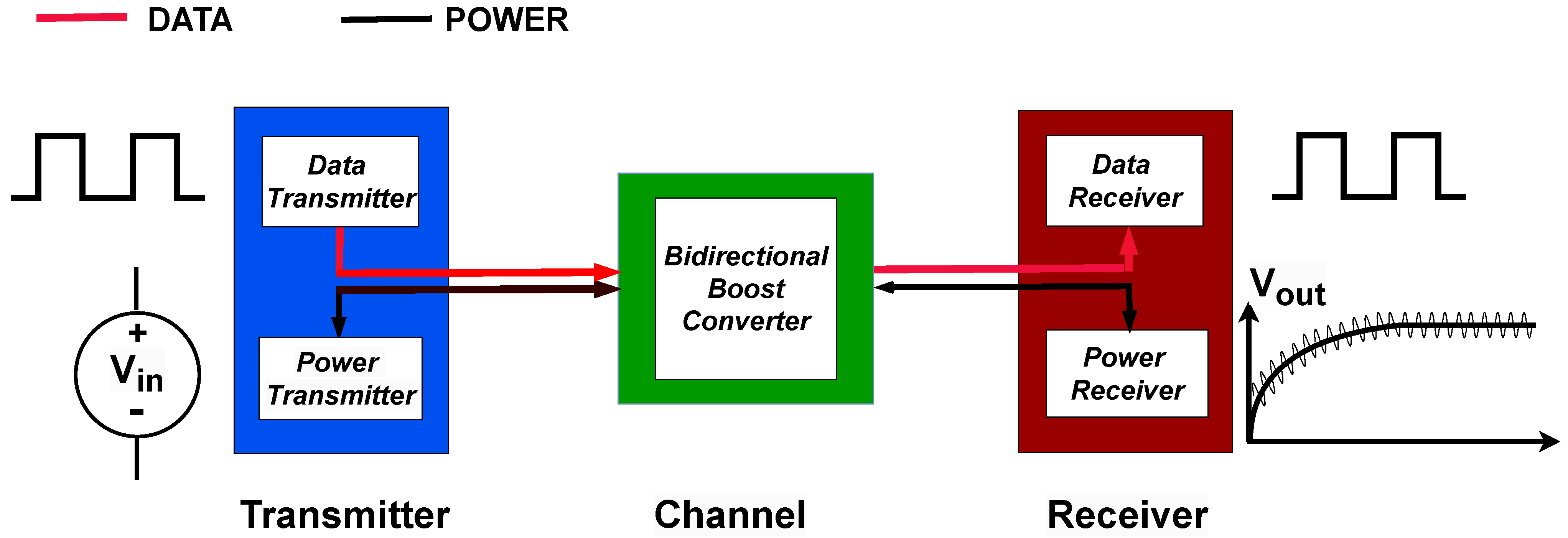
Figure 1 illustrates the block diagram of the proposed system, which integrates the TP method with a bidirectional boost converter serving as a unified channel for simultaneous power and data transmission. As shown in Figure 1, both information and power are transferred from the transmitter on the left side to the receiver on the right side. Although the transmitted data can be extracted from either the output current or voltage ripple, this paper focuses on analyzing the output voltage ripple for data detection.
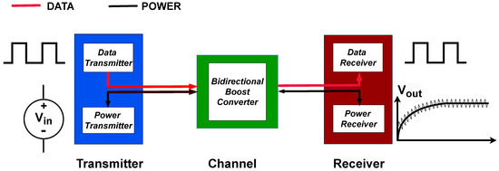
Figure 1.
Block diagram of the proposed model.
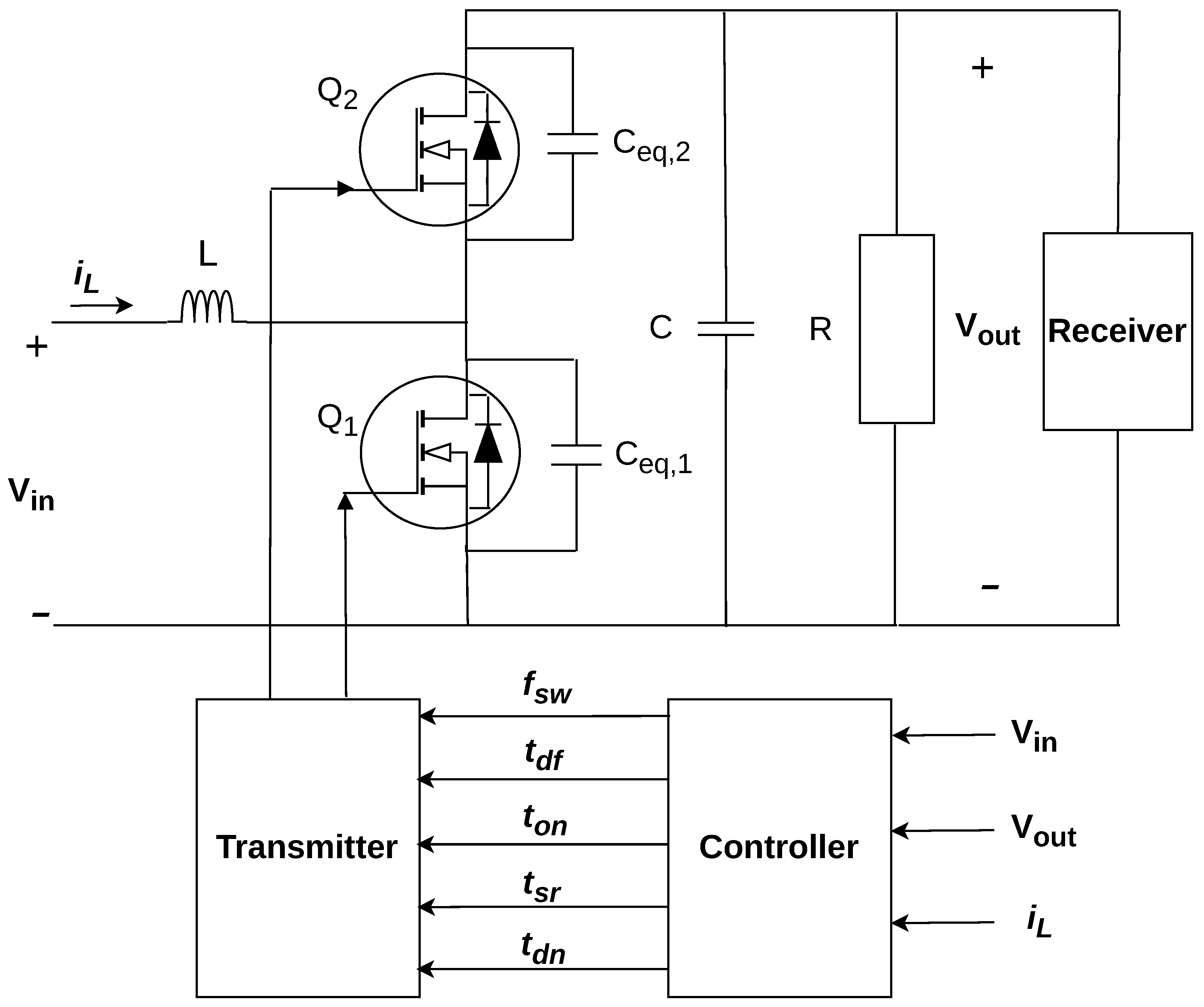
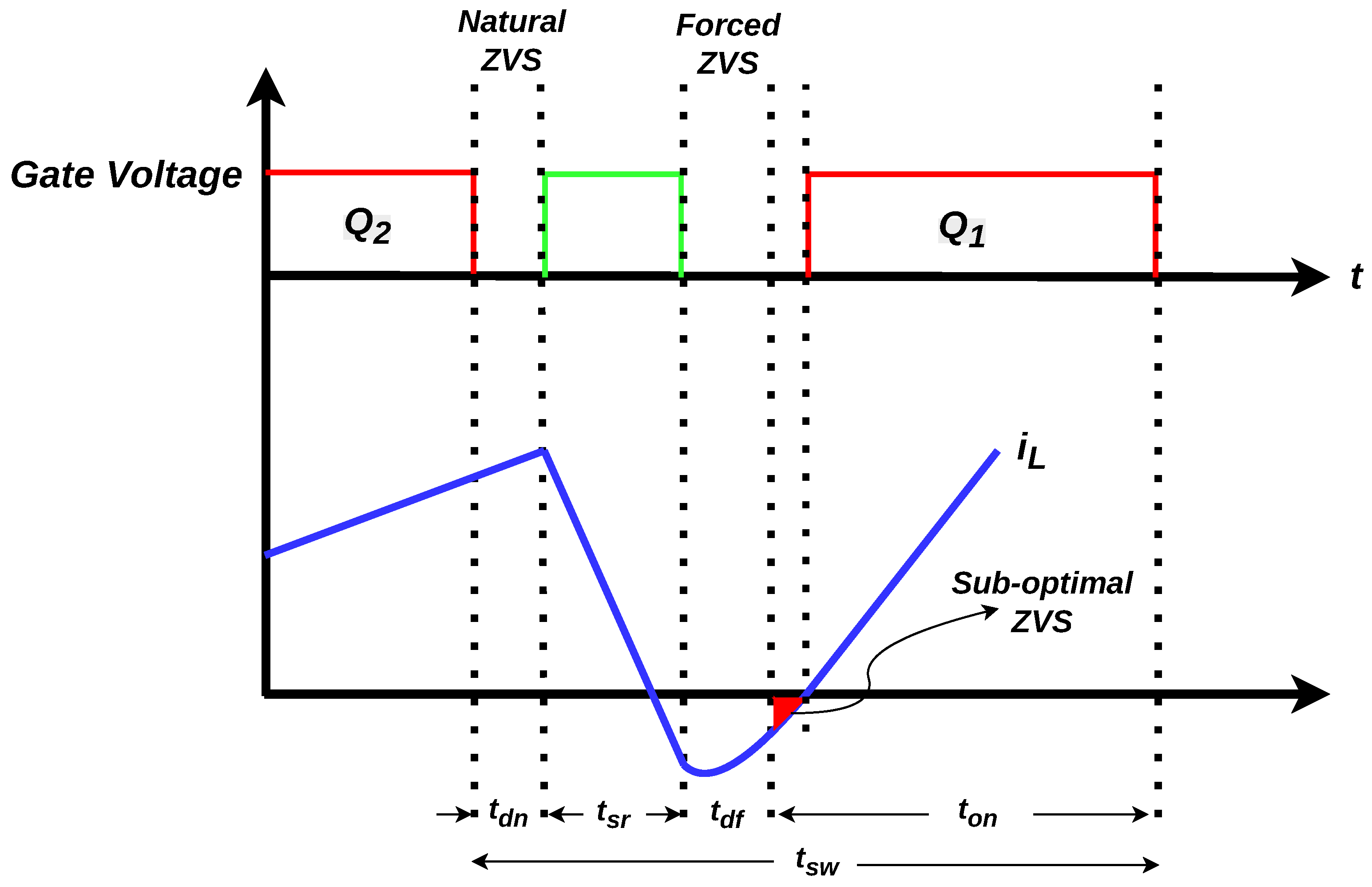
Figure 2 presents the schematic diagram of the proposed channel circuit. The main objective of the transmitter is to adjust the PWM signal for each data bit, while the main objective of the receiver is to process the output voltage to detect the transmitted data; both are discussed in detail in the following sections. The main switch can be turned on at any instant following the completion of the forced ZVS resonant interval . In the ZVS-QSW operation, the inductor current is intentionally driven negative during the resonant interval , ensuring that the synchronous rectifier switch always turns on under zero-voltage conditions after the natural resonant interval . However, excessive negative current at the turn-off instant of leads to increased circulating currents, which require higher peak currents to maintain the same average inductor current. This phenomenon results in elevated conduction losses. These losses can be minimized by optimally regulating the negative inductor current during , thereby achieving minimum conduction ZVS-QSW operation [13]. The operating waveforms of the ZVS-QSW bidirectional converter, including the key timing intervals, are illustrated in Figure 3. Maintaining this optimal state requires precise control over the timing parameters, specifically the switching period and the . and represent the combined output capacitances of the active semiconductor devices participating in the commutation process. During the dead-time interval, resonate with the main boost inductor and governs the voltage transition across the switches. Its magnitude directly affects the ZVS condition and the required natural dead-time, and therefore plays a critical role in determining switching losses and overall converter efficiency.
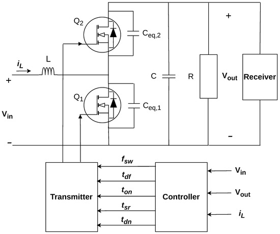
Figure 2.
Schematic diagram of the channel circuit.
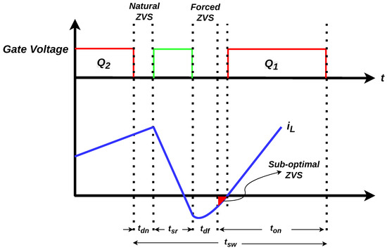
Figure 3.
ZVS-QSW operating waveforms.
Operation in this mode enables ZVS transitions with the lowest feasible negative current, significantly reducing conduction losses [13,14,15,16]. Nevertheless, this requires precise tuning of key timing parameters, particularly the switching period and the forced ZVS dead-time interval . As operating conditions vary, these parameters should be adjusted online to preserve minimum-conduction ZVS-QSW operation and to maintain optimal converter efficiency over the full operating range. Accordingly, online efficiency optimization techniques that dynamically regulate converter timing parameters have been widely adopted for both conventional SiC-based converters and wide-band-gap-based power converters. In this work, the online optimization strategy presented in [14] is employed to regulate the converter timing parameters and switching frequency.
The output voltage of the bidirectional converter in both boost and reverse power flow modes is determined using the following equations.
where is input voltage, D denotes the duty cycle of the PWM signal for switch , and denote the output voltages in boost and reverse modes, respectively. Switch is driven by a complementary PWM signal relative to switch .
Below, the ripple of the output voltage in both boost and reverse modes is analyzed. In boost mode, the total output voltage ripple arises from two main sources, the capacitive ripple and the equivalent series resistance (ESR) ripple, which can be calculated using (2) and (3), respectively.
In the above equations is the average output (load) current, C is output capacitance, is switching frequency, is the effective internal resistance of a capacitor, and and denote the voltage ripples caused by the capacitor and ESR, respectively, in boost mode. Additionally, in the above equation represents the inductor current () ripple, which can be calculated using the following equation.
where L is the inductance of the inductor. Consequently, the total output voltage ripple in boost mode can be calculated from the following equation.
Similar to boost mode, the output voltage ripple in reverse mode arises from two main sources: the capacitive ripple and the ESR ripple. While the ESR ripple in reverse mode is the same as in boost mode, the capacitive ripple differs and can be calculated using the following equations [13,14,15,16]:
Consequently, the total output voltage ripple in reverse mode can be calculated from (7).
Switching Frequency Adjustment
As can be concluded from the above equations, the output voltage ripple in both boost and reverse modes is a function of the PWM switching frequency. Consequently, by considering the switching MOSFET as a data transmitter and a receiver located on the load side, the PWM switching frequency can be used to convey data from the transmitter to the receiver. Based on the fundamentals of FSK modulation, two distinct switching frequencies can be assigned to represent the logic levels 0 and 1 of each data bit. According to (5) and (7), the only modulation scheme suitable for a bidirectional converter is FSK. This is because the output voltage ripple is independent of the phase of the transmitter. Furthermore, altering the amplitude or pulse position of the signals to implement amplitude-shift keying (ASK) or PPM is not feasible, as such changes would introduce distortions that adversely affect the operation of the bidirectional converter.
However, the most efficient method for simultaneous power and data transmission in a bidirectional converter relies on FSK modulation. The variation of the switching frequency should occur as close as possible to the optimal switching frequency. In the following, the role of the switching frequency on the functional parameters of the bidirectional converter is analyzed, and based on this analysis, an efficient method is proposed to determine the appropriate switching frequency. In the first step, the conduction loss is analyzed and calculated using the following equation:
where is the inductor RMS current, which can be calculated from (9), and represents the total equivalent series resistance of the conduction path, including the ON-state resistance of the active switches and the winding resistance (copper loss) of the main inductor.
According to (4) and (8), it can be concluded that a low leads to a large inductor RMS current, which in turn results in higher conduction losses. In the second step of the analysis, the switching loss is evaluated. The switching loss is calculated as follows [13]:
where denotes the switching power loss, refers to the equivalent output capacitance of the i-th switch, and is a shape factor (typically 0.5 for linear switching transitions). The index i corresponds to each individual MOSFET. and represent the off-state drain-source voltage and the drain current at the switching instant, respectively.
As demonstrated in (10), the switching loss is directly proportional to . Consequently, a high leads to increased switching loss. Although the steady-state voltage conversion ratio of a boost converter is primarily determined by the duty cycle, the switching frequency has a strong impact on three critical factors. First, it directly affects the inductor current ripple, which in turn influences the output voltage ripple. Second, it determines the conduction losses in both semiconductor devices and passive components. Third, it governs the switching losses associated with device capacitance. Proper selection of the switching frequency is therefore essential to balance voltage regulation and overall converter efficiency.
Based on the above switching frequency analysis, it can be concluded that should be determined through an optimization process that minimizes the output voltage ripple and total loss of the bidirectional converter, defined as the sum of conduction and switching losses. The proposed online optimization exploits this property to identify the optimal operating point without requiring prior knowledge of parasitic parameters or temperature-dependent effects.
In the proposed bidirectional boost converter, the switching frequency is adjusted through an online, measurement-based efficiency optimization process that operates in parallel with the main closed-loop voltage control. The overall control structure consists of two decoupled loops:
- Inner Control Loop (Voltage/Current Regulation): The inner loop is responsible for output voltage (or current) regulation and overall system stability. It operates using conventional PWM or QSW control and assumes the switching frequency to be constant over short time intervals. This loop ensures a fast dynamic response and robust regulation against load and input voltage variations.
- Outer Optimization Loop (Efficiency Maximization): The outer loop performs online efficiency optimization by adaptively adjusting the switching frequency. Its objective is to minimize the total converter losses while preserving stable operation guaranteed by the inner control loop.
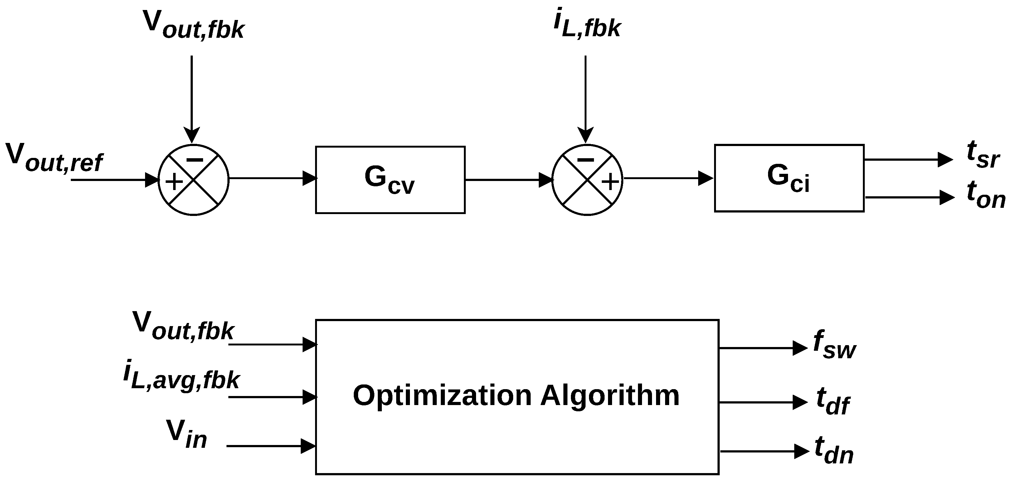
Figure 4 illustrates the detailed controller block of the TP-based bidirectional boost converter. The controller receives feedback signals from both the input and output, including the output voltage , the average inductor current and the input voltage . Based on these measurements, the optimization algorithm determines the optimal switching frequency , , , and to achieve efficient operation. In the control block diagram illustrated in Figure 4, the blocks labeled and represent the voltage and current compensators, respectively, which are implemented as standard Proportional-Integral (PI) controllers. Due to the highly nonlinear characteristics of the ZVS-QSW bidirectional converter, a two-step approach is employed to dynamically determine the requisite control variables. Initially, polynomial fit functions are utilized to correlate the real-time operating conditions with the baseline tuned parameters. Subsequently, an online optimization method is applied to fine-tune these variables and achieve the optimal soft-switching parameters. This comprehensive methodology is detailed in [14]. The optimization loop operates exclusively on empirical real-time power measurements, thereby obviating the need for complex loss modeling. At each optimization step, the converter efficiency is calculated as follows:
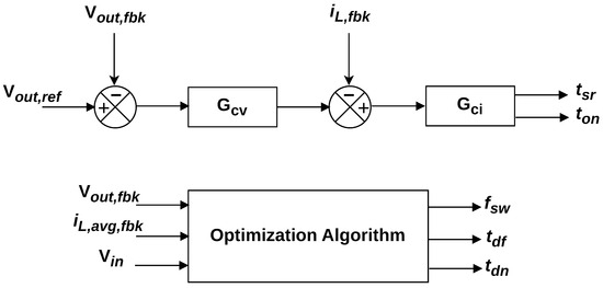
Figure 4.
Block diagram of the controller.
It is important to emphasize that because this online optimization relies exclusively on real-time empirical measurements of input and output power ( and ), all frequency-dependent losses—including both the core and copper losses of the magnetic components—are inherently captured. This model-free approach allows the system to maximize overall efficiency without requiring complex analytical loss models for the inductor. A small perturbation, as defined in (12), is applied to the switching frequency, and the resulting change in efficiency is observed:
- If the efficiency increases, the switching frequency is further adjusted in the same direction.
- If the efficiency decreases, the direction of frequency adjustment is reversed.
In the above equation, denotes the kth step of the switching frequency optimization process, and represents the applied perturbation. This process is repeated iteratively, causing the switching frequency to converge toward the value that maximizes efficiency under the current operating conditions. For more details, to systematically determine the optimal switching frequency, the online optimization algorithm evaluates a cost function, J, defined as the total power loss of the converter. The objective is to minimize this cost function by adjusting the switching frequency (), which is mathematically expressed as
To minimize this cost function, an iterative gradient-based optimization technique, such as the gradient descent algorithm, is employed. By evaluating the gradient of the measured power loss with respect to the switching frequency, the algorithm iteratively updates in the direction of the steepest descent, thereby converging to the global minimum and ensuring maximum efficiency under time-varying load conditions.
On the other hand, ZVS–QSW operation enables soft switching in bidirectional boost converters by exploiting the resonant interaction between the main boost inductor and the intrinsic output capacitances of the power semiconductor devices during the dead-time interval. Zero-voltage turn-on is achieved when the energy stored in the inductor is sufficient to completely discharge the equivalent switch capacitance prior to turn-on, with the required natural dead-time being inversely proportional to the inductor current. This operating principle significantly reduces turn-on switching losses and electromagnetic interference, thereby enabling efficient operation at higher switching frequencies without the need for additional resonant components. As a result, ZVS–QSW operation improves overall efficiency, increases power density, and remains fully compatible with bidirectional power flow. Since ZVS feasibility strongly depends on the operating point, the switching frequency can be adaptively adjusted to maintain ZVS–QSW operation while balancing conduction and switching losses over a wide range of load and voltage conditions.
To avoid interaction between regulation and optimization, the switching frequency is updated on a significantly slower time scale than the inner control loop. This separation of time scales ensures that voltage regulation remains stable while the efficiency optimization gradually adapts the operating frequency. In the proposed bidirectional boost converter, the switching frequency is controlled through a model-free, online efficiency optimization loop that perturbs the frequency based on measured efficiency [15]. Consequently, the previously introduced control parameters are updated synchronously with the switching frequency to maintain system consistency. By decoupling frequency optimization from voltage regulation, the control strategy guarantees both high efficiency and stable closed-loop performance across a wide range of operating conditions.
3. Efficient Data Transmitter and Optimal Data Receiver Design
Information transmission and reception are critical components of TP technology, particularly in systems where power delivery performance should be preserved. Inadequate transmission strategies or suboptimal modulation techniques can adversely affect power transfer, leading to reduced efficiency or operational disturbances. Conversely, the ability to reliably receive and accurately detect transmitted information has a direct impact on the overall efficiency and robustness of TP systems. Accordingly, the following subsections examine the design considerations of an efficient data transmitter and an optimal data receiver.
3.1. Efficient Data Transmitter Design
As discussed earlier, variations in bidirectional boost converter parameters such as phase, amplitude, and pulse width introduce significant distortion in power transmission, making them unsuitable for reliable data encoding. In practice, information transfer in a bidirectional boost converter can be effectively achieved through modulation of the switching frequency; therefore, FSK modulation is adopted in this work. Consequently, in this study, the switching frequency is utilized as the sole information-bearing variable to encode data, as described by (5) and (7).
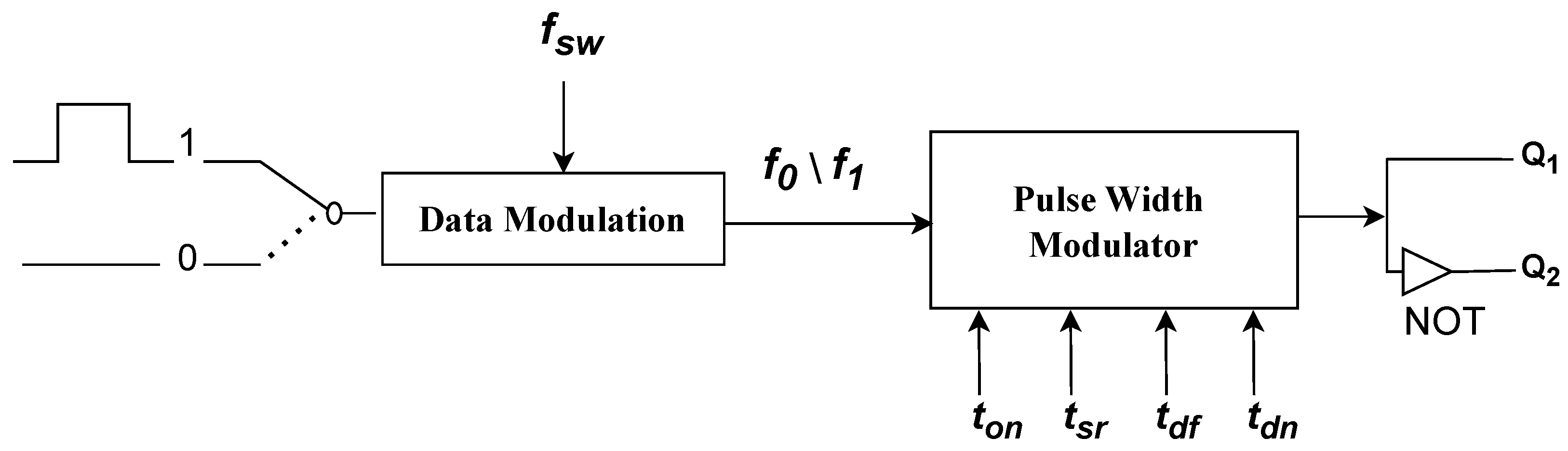
The transmitter encodes binary information by assigning distinct values of the switching frequency to represent logic states ‘0’ and ‘1’. By modulating at the transmitter, the receiver can distinguish between the two states by analyzing the resulting output voltage ripple. Figure 5 illustrates the schematic of the proposed data transmitter. The optimal switching frequencies that maximize energy efficiency are determined using the online efficiency optimization technique described earlier. Based on this optimization, the frequencies and are calculated from (14) to represent logic ‘0’ and ‘1’, respectively.
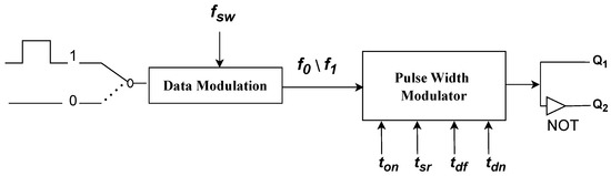
Figure 5.
Block diagram of the transmitter.
In (14), represents the deviation of or from the optimal . The frequencies and differ only slightly from the optimal switching frequency to ensure that power transmission efficiency is not significantly reduced. Since the optimal changes with variations in load or other parameters of the bidirectional boost converter, the transmitter should adaptively adjust and to maintain maximum efficiency.
According to (5) and (7), increasing the difference between and enhances the distinguishability of the resulting output voltage ripple , improving data detection at the receiver. Therefore, is chosen to be as small as possible to preserve efficiency. However, under higher noise conditions, should be increased to ensure reliable detection of transmitted data at the receiver.
3.2. Optimal Data Receiver Design
To optimize the data receiver design, it is essential to account for the unknown values of the bidirectional boost converter circuit components at the receiver side. This consideration is critical to maintaining the efficiency of the proposed TP model over a wide range of load conditions, particularly in charging applications. A key requirement is that the load should reliably distinguish between the transmissions corresponding to and through detailed analysis of the output voltage . Accordingly, the differences between and transmissions manifest as distinguishable ripple characteristics in , which can be exploited for robust data detection.
Due to the uncertainty of parameters within the receiver and the presence of a time-varying load, along with the critical requirement for adaptive operation under circuit variations, conventional maximum likelihood methods are often ineffective. Furthermore, since depends on multiple interrelated parameters, the resulting information detection problem is inherently nonlinear and complex. By introducing reasonable simplifications, can be approximated as a function of the duty cycle D, capacitance C, and inductance L. To address these challenges, this paper employs a supervised learning-based classification approach to accurately extract the transmitted information encoded as and within the signal.
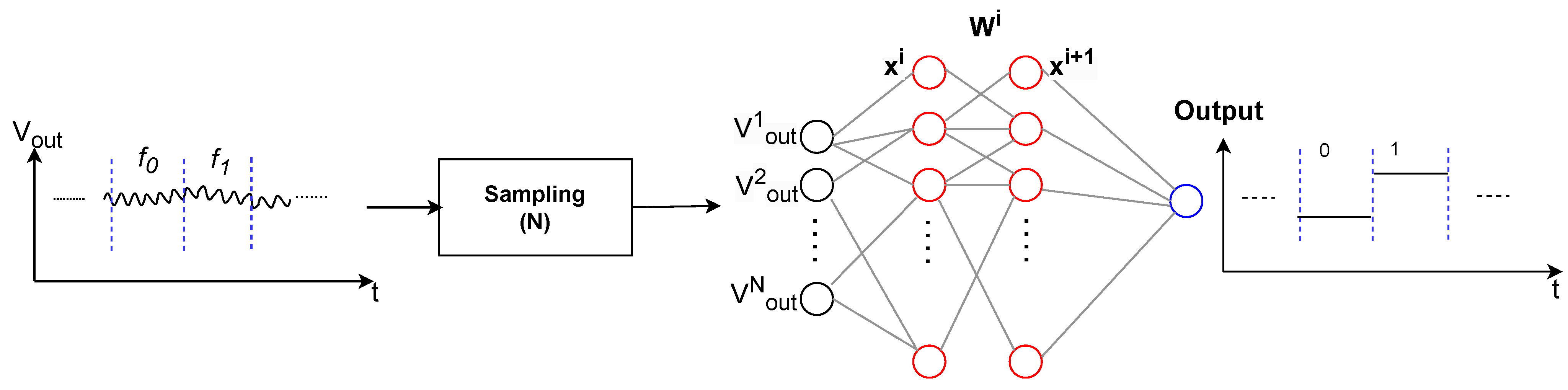
In this study, a multi-layer NN was employed to analyze samples and identify the transmitted symbols, or . The NN’s input layer consists of N neurons, where N corresponds to the number of samples collected during the transmission of each switching frequency symbol over a time interval . The hidden layers are configured with twice the number of neurons as the input layer, while the output layer comprises a single neuron. The sign of the output neuron determines whether or was transmitted. The architecture and depth of the hidden layer were determined empirically to strike an optimal balance between classification accuracy and computational complexity. Since the proposed method is intended for practical execution on standard Microcontroller Units (MCUs) or Digital Signal Processors (DSPs), minimizing the computational load is essential. Experimental evaluations indicated that a single hidden layer provides sufficient detection robustness, whereas increasing the network depth yields only marginal improvements in accuracy at the cost of a disproportionately higher computational load.
The network architecture, illustrated in Figure 6, corresponds to a fully connected NN. Inter-layer connectivity is realized through the activation function, specifically the hyperbolic tangent, such that the neuron values in each layer depend on those in the preceding layer. Let denote the vector of neurons in the i-th layer, and let represent the corresponding weight matrix. Prior to its use as an information detector, the NN should undergo a training process, during which the weights are iteratively adjusted to ensure that changes in the input layer produce the desired output. The training process begins with randomly initialized weights, which are subsequently optimized using gradient descent in combination with backpropagation [17]. The NN is trained to classify signals into two relative categories: the lower and higher frequency states of the FSK modulation. By focusing on these relative ripple differences rather than absolute values, the detection remains robust even as the baseline switching frequency is shifted by the efficiency optimizer.
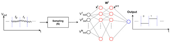
Figure 6.
NN detector of the data receiver: samples are utilized in the first layer and bit 0 or 1 is detected as output in the last layer.
During training, the NN is presented with a dataset of signal samples corresponding to various circuit parameters L, C, and (, ) pairs. The network is trained to map these inputs to their respective ideal responses, represented by the transmitted switching frequency symbols. Through iterative adjustments, the weights of neurons across all layers gradually converge to their optimal configurations. It is important to note that information detection is not confined to steady-state samples; the NN is extensively trained to extract critical insights from transient behaviors, such as over or undershooting events, thereby significantly expanding the scope of data analysis and interpretation.
Upon completion of the training phase, the network demonstrates high proficiency, producing accurate outputs with minimal error across a wide range of input variations. The accuracy of the network during testing is influenced by several factors, including the quality and diversity of the dataset. A rich and uncorrelated dataset not only improves weight optimization during training but also brings the network closer to the ideal performance. Another key factor is the number of samples; increasing the sample size enhances the network’s ability to detect underlying patterns and effectively distinguish between and transmissions.
To evaluate the practical feasibility of the system, the computational complexity of the proposed neural network is systematically analyzed. The implemented receiver NN comprises three layers, with N, , and 1 denoting the number of neurons in the input, hidden, and output layers, respectively. During the feed-forward inference process, each of the hidden neurons computes the weighted sum of the N input values. The resulting sum is then passed through the activation function, which imposes a constant computational cost per neuron. Subsequently, the outputs of the hidden layer are weighted, summed, and fed into the single output neuron, which applies a final activation. Consequently, the total computational complexity of the feed-forward process scales as , which asymptotically simplifies to . Furthermore, during the offline training phase, the complexity of the back-propagation algorithm must be considered. The back-propagation process involves calculating the error gradients, multiplying them by the corresponding synaptic weights, and updating the network parameters. This procedure demands a computational effort that strictly mirrors the feed-forward process. Therefore, the computational complexity during training is effectively doubled per data point, as both feed-forward and back-propagation operations must be iteratively executed for every sample in the training dataset. It should be noted that the training process of the NN—which is comprehensively detailed in the manuscript—can be performed entirely offline. Once the network is trained, executing the model (inference) to achieve data detection is easy as the model is computationally lightweight.
SNR generally plays a crucial role in information detection and is a key parameter that strongly influences detection accuracy. To calculate the SNR, we first determine the power of the noise. The thermal noise can be expressed as
where K is the Boltzmann constant, T is the temperature, and B is the bandwidth. From (5) and (7), which equal to amplitude of the desired signal, it is evident that the noise power is significantly lower than the signal power, justifying the assumption of a high SNR, for which the probability of error approaches zero. In low-SNR scenarios, performance can be improved by increasing the time interval or the number of samples, thereby enhancing the integration process.
It is worth noting that the above design is intended for the transmission of a single bit; however, it is fully compatible with multi-bit transmission. In multi-bit configurations, additional transmission frequency indices are employed, and the number of output-layer neurons corresponds to the number of transmitted bits.
4. Real-Time Simulations and Verification
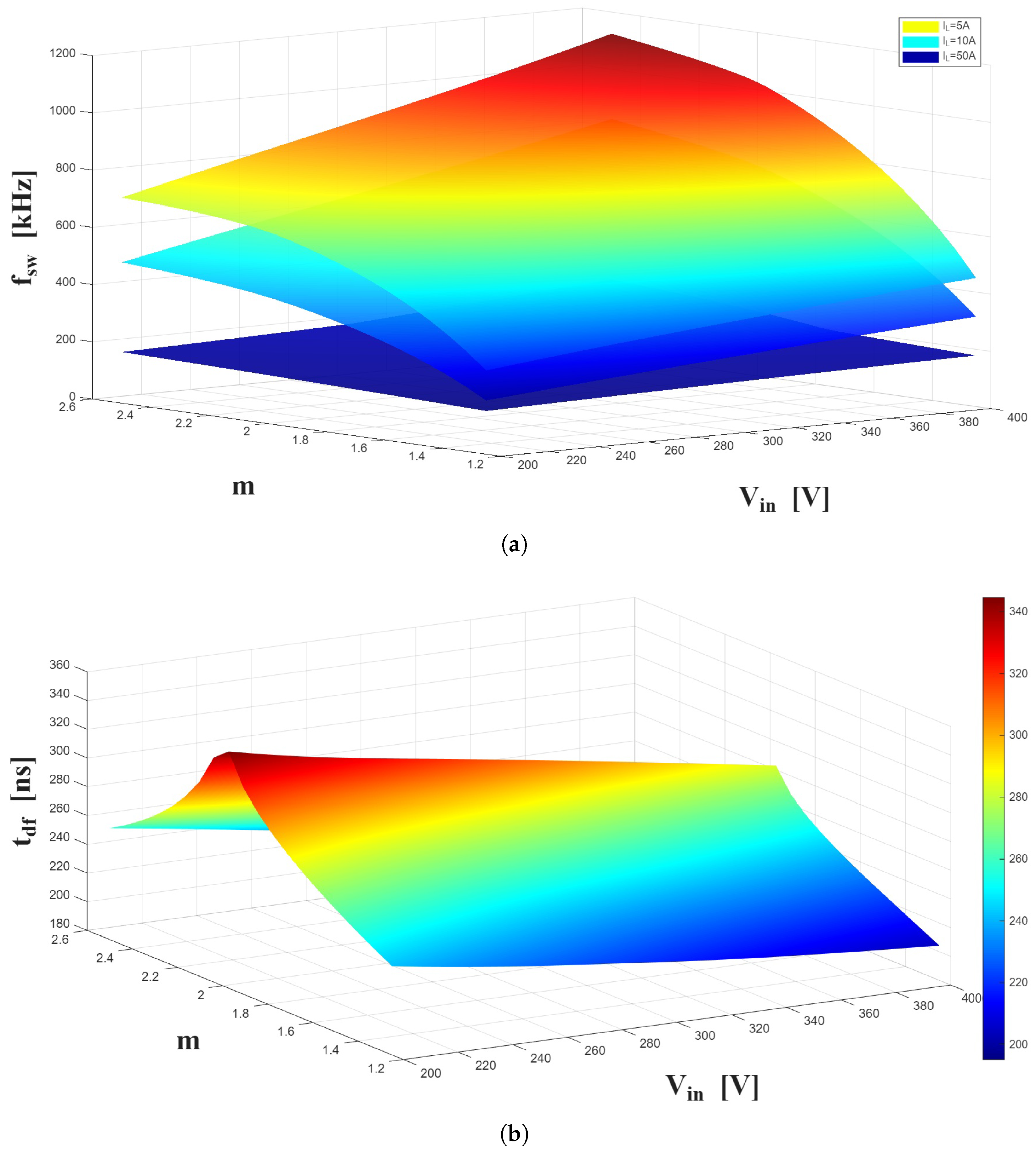
This section presents the simulation studies conducted on the proposed data transmitter and receiver designs. As summarized in Table 1, the output voltage is varied to demonstrate the robustness of the proposed scheme in accurately detecting transmitted information under load fluctuations. Parameter m in Table 1 is a conversion ratio which equals to . Figure 7 illustrates the optimal and of the bidirectional boost converter as a function of and m. The switching frequency values shown in this figure are obtained after the controller reaches a steady and reliable operating state. Based on this analysis, the frequency deviation is selected as 5 KHz, and the corresponding values of and are subsequently determined using (14). By substituting and in place of the optimal switching frequency (shown in Figure 7a) into the above equation, the system efficiency can be calculated using (11), yielding a value close to 98%. Considering that the efficiency of the bidirectional boost converter without TP technology is already near this level, it can be concluded that the design presented in this paper approaches the optimal performance. For a comprehensive analysis, the 600 V output voltage limit for , as specified in Table 1, was not enforced in the simulation results shown in Figure 7.

Table 1.
Simulation Parameters.
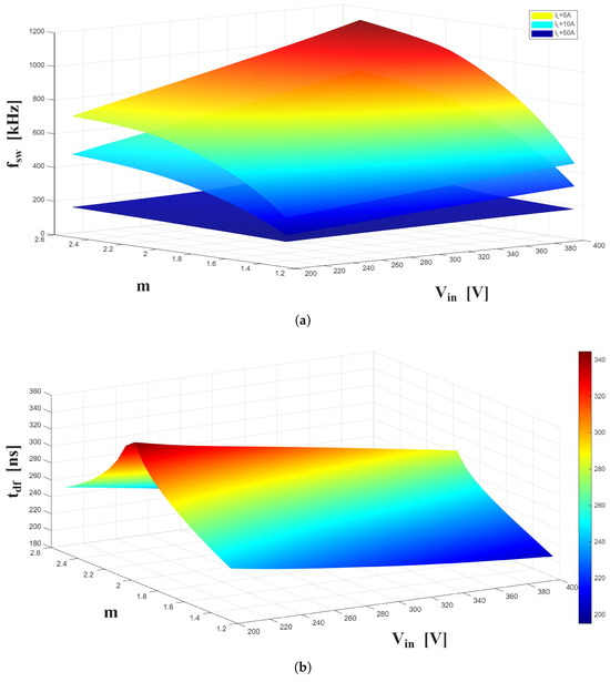
Figure 7.
(a) Optimal value of as a function of m and ; (b) Optimal as a function of m and in TP based bidirectional boost converter.
In the following subsections, simulations of the receiver operation are carried out under two distinct scenarios, denoted as Scenario A and Scenario B.
4.1. Scenario A
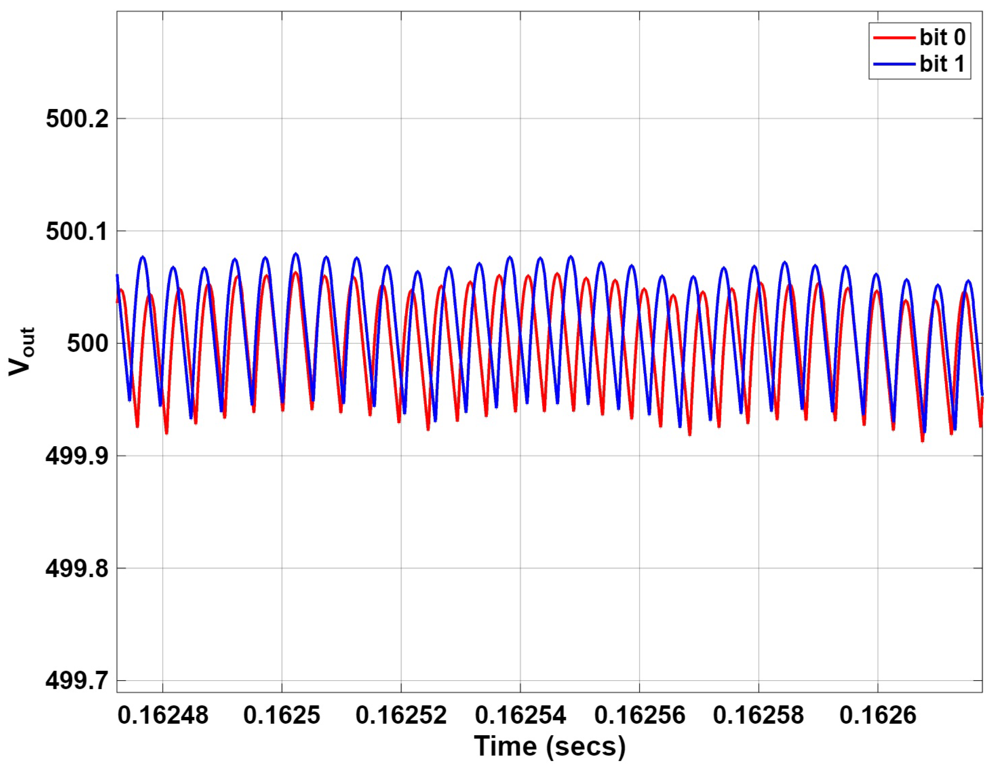
In this scenario, simulations were performed in Simulink to implement the model presented in Figure 1, including the transmitter, receiver, controller, and bidirectional boost converter, thereby producing a variety of outputs for analysis. Figure 8 shows the variation of for the two transmission states and . Notably, the ripple characteristics differ between and (corresponding to bit 0 and bit 1), both in terms of the ripple pattern and the amplitude magnitude. As discussed previously, accurate classification of the transmitted bit requires training the N with a comprehensive dataset. To construct this dataset, multiple circuit configurations were generated by varying component values up to ±25% from those listed in Table 1. It is important to note that the classification accuracy improves with increased dataset size and diversity. In this study, a total of 20,000 training data points were employed. For each circuit transmitting the and pair, the corresponding signals were recorded and used for NN training. Consequently, four distinct information transmission modes—00, 01, 10, and 11—were identified, each corresponding to a unique pattern. During NN training, however, these modes were processed in a single-bit format. This approach enhances the network’s learning capability, reducing classification errors when consecutive bits are identical compared to sequences of non-identical bits.
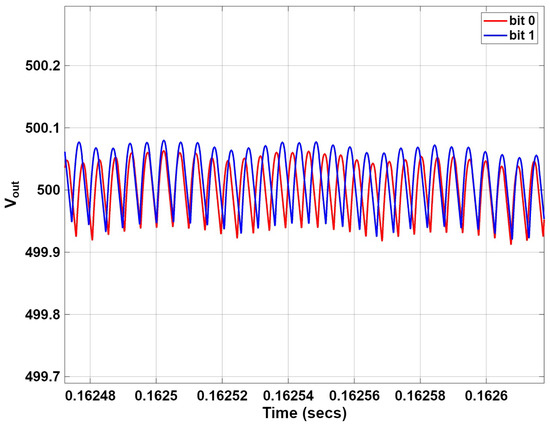
Figure 8.
of two state transmission and multiple controller adjustment cycles. Blue signal related to transmission and red signal related to transmission: both the patterns concealed within the ripple and the magnitude of the ripple amplitude are different for each signal.
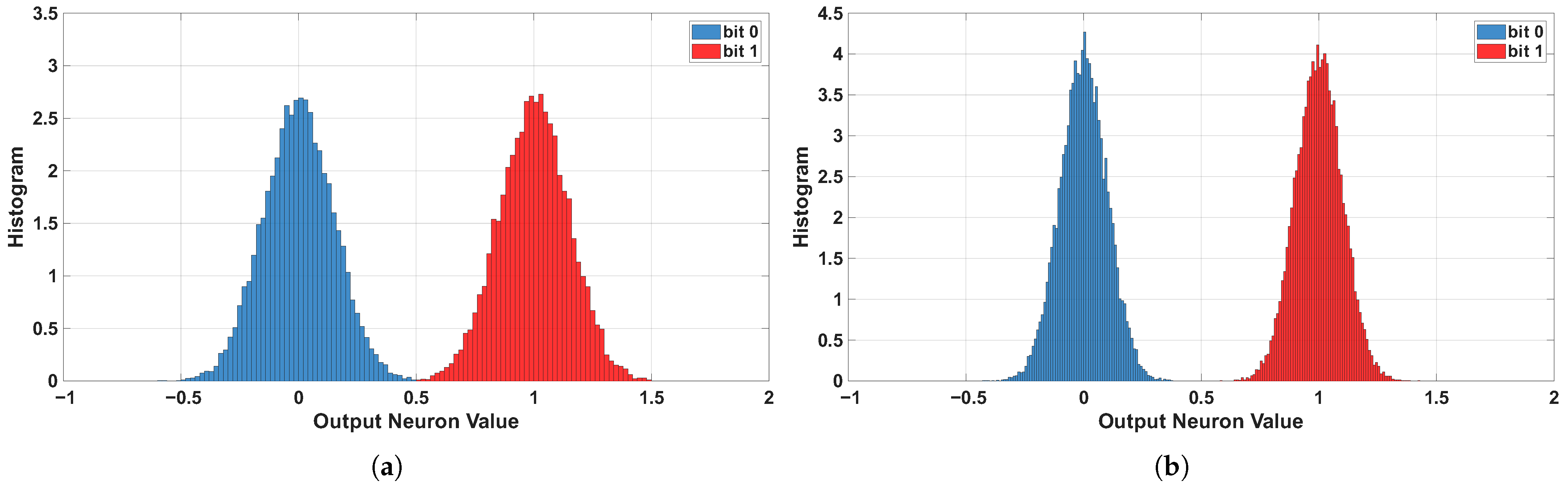
Figure 9 presents a histogram of the output neuron values of the NN’s final layer, based on 5000 test data points. In the figure, bit 1 is represented on the right and bit 0 on the left. The results indicate that the detector accurately identifies the transmitted information. The detection effectiveness is strongly correlated with the distance of the final-layer neuron values from zero for both bit states. Notably, the ripple—affected not only by and but also by circuit component variations—plays a key role in detection performance. Cases where the neuron value approaches zero typically occur when specific L and C values minimize the ripple, thereby reducing detection accuracy. Improved performance is observed with an increased number of hidden layers in the NN. For the simulations, two hidden layers were employed to evaluate the detector’s performance. The detection accuracy improves with an increasing number of samples, as illustrated by the comparison between Figure 9a,b. However, higher sample counts result in increased computational complexity. To address this trade-off while maintaining performance, a practical approach is to isolate portions of the signal that exhibit strong similarity across both transmission modes ( and ) for subsequent sampling. This similarity is most pronounced in the transient-state region of .
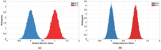
Figure 9.
Histogram of the neuron values of the NN’s last layer based on 5000 test data points and 20,000 training data points: (a) for N = 500 samples and (b) for N = 1000 samples.
4.2. Scenario B
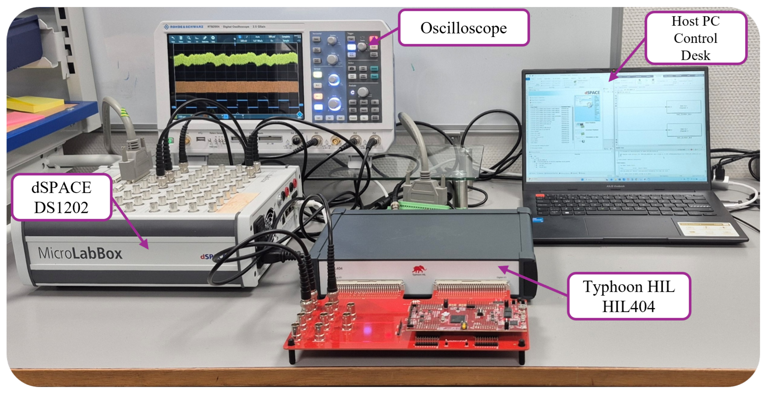
In this scenario, a real-time Hardware-in-the-Loop (HiL) simulation was conducted to validate the feasibility of the proposed TP technique in the bidirectional boost converter circuit. The experimental setup, shown in Figure 10, employs the dSPACE MicroLabBox Real-Time Target Machine in conjunction with Simulink, providing a versatile platform for investigating and implementing design principles in mechatronics, motion control, power electronics, and signal processing. In this scenario, a real-time HiL simulation was conducted to validate the feasibility of the proposed TP technique in the bidirectional boost converter circuit. The experimental setup employs a dSPACE MicroLabBox real-time system in conjunction with MATLAB/Simulink R2025b, providing a flexible and widely adopted platform for real-time control and power electronics applications.
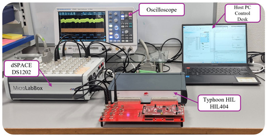
Figure 10.
Details of the experimental setup based on dSPACE Real-Time Target Machine.
The dSPACE MicroLabBox integrates a high-performance multi-core processor together with programmable FPGA-based I/O, enabling deterministic real-time execution of control algorithms and fast signal acquisition. The real-time application is automatically generated from Simulink models using dSPACE’s real-time interface and executed on the MicroLabBox target with fixed-step solvers. Analog and digital I/O channels are used to interface the converter model, controller, and measurement signals, ensuring accurate emulation of the bidirectional boost converter dynamics under real-time constraints. This setup enables closed-loop validation of the proposed data transmission and reception strategy while preserving timing accuracy and computational determinism [27,28].
Using this setup, the circuit and control architecture described in this paper were implemented and evaluated in real time, confirming the validity of the simulation results and demonstrating the effectiveness of the proposed TP-based bidirectional boost converter under realistic operating conditions. Specifically, the bidirectional boost converter was emulated in the Typhoon HIL, while the remaining system components, including the controller, transmitter, and receiver blocks, were implemented on the dSPACE platform.
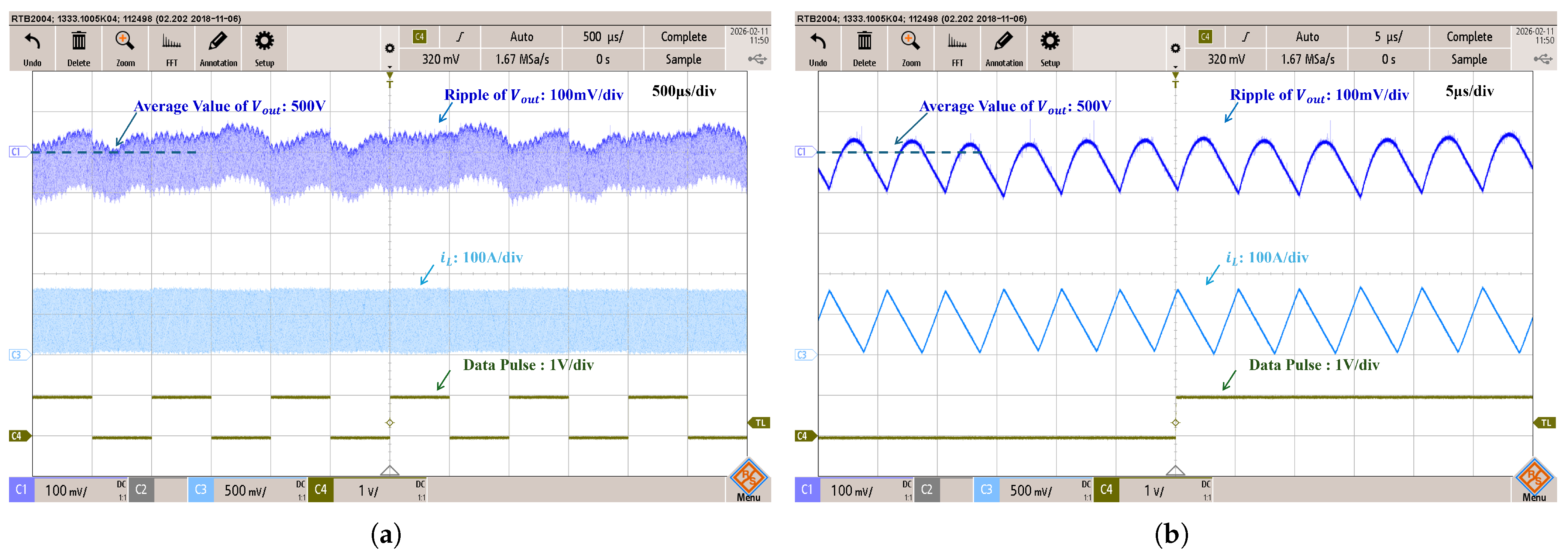
The HiL results under steady-state are shown in Figure 11. The output voltage, inductor current, and data bit are illustrated in this figure. Figure 11b presents a zoomed-in view of Figure 11a at the instant when the transmitted bit transitions from 0 to 1. Since the frequency deviation, , is relatively small (approximately 5 kHz) compared to the switching frequency, kHz, the output voltage ripple varies smoothly, and no noticeable overshoot or undershoot occurs during the bit transition. In contrast, for larger values of , the variation in the output ripple becomes less smooth. Furthermore, as expected, the amplitude of the output voltage ripple is less than 1% of the nominal output voltage, which is acceptable for simultaneous power and data transmission through the inductor current. Overall, the real-time HiL simulations validate the effectiveness of the proposed TP technique, demonstrating that the bidirectional boost converter sustains a high power transfer efficiency approaching 98% under realistic operating conditions.
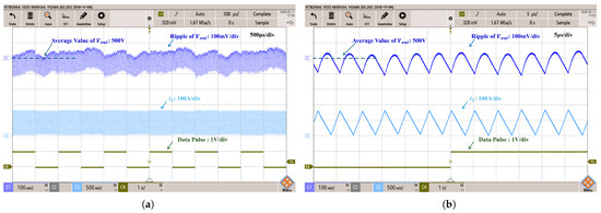
Figure 11.
(a) HiL steady-state results of , with = 200 KHz and = 5 KHz; (b) a zoomed-in view results during a 0-to-1 bit transition.
5. Conclusions
In this paper, we investigated the application of TP technology for the simultaneous transmission of power and information in adaptive scenarios, using a high-frequency bidirectional boost converter based on a SiC ZVS-QSW topology. A primary focus was the efficient design of both the data transmitter and receiver, key components of TP systems. Data encoding was achieved through the switching frequency, which was carefully chosen to maximize energy efficiency by employing closed-loop online optimization, with only minor adjustments to the switching frequency. To ensure practical relevance, the proposed model assumes that charging devices operate without knowledge of the converter parameters and may experience varying loads during operation, necessitating adaptive transmission of both power and data. The design of the optimal data receiver employed an NN-based classification algorithm, enabling accurate detection of information embedded in the output voltage ripple.
Simulation results confirmed the effectiveness of the proposed system, demonstrating its ability to seamlessly handle simultaneous power and data transmission. This work addresses the limitations of previous methods and highlights the practical potential of TP technology. Future work will explore the integration of advanced machine learning and artificial intelligence techniques to further optimize the design of TP transmitters and receivers for a wide range of applications.
Author Contributions
Conceptualization, S.A.M.; Methodology, S.A.M.; Software, A.M.; Validation, A.M. and M.H.K.; Formal analysis, S.A.M. and A.M.; Resources, S.A.M.; Data curation, S.A.M.; Writing—original draft, S.A.M.; Writing—review & editing, S.A.M. and M.H.K.; Visualization, S.A.M.; Supervision, M.H.K.; Funding acquisition, M.H.K. All authors have read and agreed to the published version of the manuscript.
Funding
This research was funded by Aarhus University Research Foundation, AUFF-E-2023-9-60.
Data Availability Statement
The original contributions presented in this study are included in the article. Further inquiries can be directed to the corresponding authors.
Acknowledgments
During the preparation of this manuscript, the authors used Gemini 3 Flash to refine the linguistic clarity and verify the grammatical accuracy of the text. The authors have reviewed and edited the output and take full responsibility for the content of this publication.
Conflicts of Interest
The authors declare no conflicts of interest.
References
- Liserre, M.; Beiranvand, H.; Leng, Y.; Zhu, R.; Hoeher, P.A. Overview of Talkative Power Conversion Technologies. IEEE Open J. Power Electron. 2023, 4, 67–80. [Google Scholar] [CrossRef]
- He, X.; Wang, R.; Wu, J.; Li, W. Nature of power electronics and integration of power conversion with communication for talkative power. Nat. Commun. 2020, 11, 2479. [Google Scholar] [CrossRef]
- Leng, Y.; Zhu, R.; Beiranvand, H.; Liserre, M.; Hoeher, P.A. Review of Coding Theory and Applications of Switching Ripple-based Talkative Power Converters. In Proceedings of the 2022 IEEE 13th International Symposium on Power Electronics for Distributed Generation Systems (PEDG), Kiel, Germany, 26–29 June 2022; IEEE: New York, NY, USA, 2022; pp. 1–6. [Google Scholar] [CrossRef]
- Hoeher, P.A.; Leng, Y.; Zhu, R.; Liserre, M. Talkative Power Conversion: A Tutorial. Proc. IEEE 2025, 113, 344–369. [Google Scholar] [CrossRef]
- Hoeher, P.A.; Mewis, M.; Liserre, M. Channel Coding and Receiver Design for Simultaneous Wireline Information and Power Transfer. IEEE Open J. Power Electron. 2021, 2, 545–558. [Google Scholar] [CrossRef]
- Leng, Y.; Zhu, R.; Liserre, M.; Hoeher, P.A. Variable Zero-Vector-Width-Based Three-Phase DC/AC Talkative Power Conversion. IEEE J. Emerg. Sel. Top. Power Electron. 2024, 12, 3402–3414. [Google Scholar] [CrossRef]
- Mönch, S.; Kuring, C.; Geng, X.; Hoeher, P.A.; Liserre, M.; Quay, R.; Dieckerhoff, S. Efficient Talkative Power Conversion with Quasi-Square-Wave Zero-Voltage Switching Hysteretic Current Control. IEEE Trans. Power Electron. 2023, 38, 12383–12387. [Google Scholar] [CrossRef]
- Guan, Y.; Wu, J.; Liu, K.; Zhao, K.; He, X. Multi-Input PV Optimizer System with Built-in Communication using Talkative Power Conversion. IEEE J. Emerg. Sel. Top. Power Electron. 2024, 12, 3392–3401. [Google Scholar] [CrossRef]
- Wang, F.; Yuan, D.; Zhang, X. Low Voltage Inbound Powerline Communication Based on Talkative Power Conversion. IEEE J. Emerg. Sel. Top. Power Electron. 2024, 12, 3348–3359. [Google Scholar] [CrossRef]
- Liu, K.; Yang, H.; Chen, Y.; Hui, Y.; Wu, J.; He, X. Active Rectified LLC Resonant Converter Using Combined Frequency and Phase Modulation for Talkative Power Conversion. IEEE J. Emerg. Sel. Top. Power Electron. 2024, 12, 3315–3324. [Google Scholar] [CrossRef]
- Hui, Y.; Tang, K.; Liu, K.; Chen, Y.; Wu, J.; He, X. Power and Signal Dual Modulation in DC/DC Converters Using FSK-Based DSSS for High Anti-Interference Performance. IEEE Trans. Power Electron. 2026, 41, 3712–3725. [Google Scholar] [CrossRef]
- Mietzner, J.; Chakraborty, C.; Hoeher, P.A.; Lampe, L. Comprehensive Signal Modeling for Talkative Power Conversion. IEEE Access 2025, 13, 111098–111114. [Google Scholar] [CrossRef]
- Luo, F.L.; Ye, H. Advanced DC/DC Converters; CRC Press: Boca Raton, FL, USA, 2024. [Google Scholar] [CrossRef]
- Sankaranarayanan, V.; Gao, Y.; Erickson, R.W.; Maksimovic, D. Online Efficiency Optimization of a Closed-Loop Controlled SiC-Based Bidirectional Boost Converter. IEEE Trans. Power Electron. 2022, 37, 4008–4021. [Google Scholar] [CrossRef]
- Maksimovic, D. Design of the zero-voltage-switching quasi-square-wave resonant switch. In Proceedings of IEEE Power Electronics Specialist Conference—PESC ’93, Seattle, WA, USA, 20–24 June 1993; IEEE: New York, NY, USA, 1993; pp. 323–329. [Google Scholar] [CrossRef]
- Majmunović, B.; McDonald, B.A.; Yu, S.-Y.; Strydom, J. 90∘-Valley Unified Controller for Zero-Voltage-Switching Quasi-Square-Wave (ZVS-QSW) Boost Converter. IEEE Trans. Power Electron. 2024, 39, 6930–6940. [Google Scholar] [CrossRef]
- Mousavi, S.A.; Izadi, Z.G.; Khooban, M. Applications of Deep Machine Learning in Future Energy Systems; Elsevier: Amsterdam, The Netherlands, 2024; Chapter 9. [Google Scholar]
- Mousavi, S.A.; Izadi, Z.G.; Khooban, M. Empowering Talkative Power Technology in Wireless Power Transfer with Machine Learning. IET Power Electron. 2024, 17, 3083–3092. [Google Scholar] [CrossRef]
- He, X.; Liu, S.; Wu, J.; Feng, Y.; Wang, R.; Li, W.; Weng, W. Wireless power and information dual transfer system via magnetically coupled resonators. Commun. Eng. 2024, 3, 8. [Google Scholar] [CrossRef]
- Taherinejad, N.; Lampe, L.; Mirabbasi, S. An Adaptive Impedance-Matching System for Vehicular Power Line Communication. IEEE Trans. Veh. Technol. 2017, 66, 927–940. [Google Scholar] [CrossRef]
- Kim, D.-S.; Lee, S.-Y.; Wang, K.-Y.; Choi, J.-C.; Chung, D.-J. A Power Line Communication Modem Based on Adaptively Received Signal Detection for Networked Home Appliances. IEEE Trans. Consum. Electron. 2007, 53, 864–870. [Google Scholar] [CrossRef]
- Miao, M.; Wang, L.; Chen, G. Design and Performance Analysis of an Adaptive-MDCSK System Over Katayama Power Line Communication Channel. IEEE Trans. Commun. 2025, 73, 8747–8755. [Google Scholar] [CrossRef]
- Eldar, Y.C.; Goldsmith, A.; Gündüz, D.; Poor, H.V. (Eds.) Machine Learning and Wireless Communications; Cambridge University Press: Cambridge, UK, 2022. [Google Scholar]
- He, R.; Ding, Z. Applications of Machine Learning in Wireless Communications; Institution of Engineering and Technology: Stevenage, UK, 2019. [Google Scholar]
- Huang, J.; Lan, M.; Zhang, H.; Huang, C.; Zhang, W.; Cui, S. Design of Noncoherent Communications: From Statistical Method to Machine Learning. IEEE Wirel. Commun. 2020, 27, 76–83. [Google Scholar] [CrossRef]
- Siegel, B. Industrial Anomaly Detection: A Comparison of Unsupervised Neural Network Architectures. IEEE Sens. Lett. 2020, 4, 7501104. [Google Scholar] [CrossRef]
- Hajihosseini, M.; Andalibi, M.; Gheisarnejad, M.; Farsizadeh, H.; Khooban, M.-H. DC/DC Power Converter Control-Based Deep Machine Learning Techniques: Real-Time Implementation. IEEE Trans. Power Electron. 2020, 35, 9971–9977. [Google Scholar] [CrossRef]
- Amin, M.; Aziz, G.A.A.; Durkin, J.; Mohammed, O.A. A Hardware-in-the-Loop Realization of Speed Sensorless Control of PMa-SynRM with Steady-State and Transient Performances Enhancement. IEEE Trans. Ind. Appl. 2019, 55, 5331–5342. [Google Scholar] [CrossRef]
Disclaimer/Publisher’s Note: The statements, opinions and data contained in all publications are solely those of the individual author(s) and contributor(s) and not of MDPI and/or the editor(s). MDPI and/or the editor(s) disclaim responsibility for any injury to people or property resulting from any ideas, methods, instructions or products referred to in the content. |
© 2026 by the authors. Licensee MDPI, Basel, Switzerland. This article is an open access article distributed under the terms and conditions of the Creative Commons Attribution (CC BY) license.