Article

A Graded Partial Dielectric Transformer for Bandwidth Enhancement in an Ultrawideband High-Power Combined TEM Antenna


by
Alexander D. Dowell
,
Mohamed Z. M. Hamdalla
* and
Kalyan C. Durbhakula
Missouri Institute for Defense and Energy, University of Missouri-Kansas City, Kansas City, MO 64110, USA
*
Author to whom correspondence should be addressed.
Telecom 2026, 7(3), 54; https://doi.org/10.3390/telecom7030054
Submission received: 11 March 2026 / Revised: 22 April 2026 / Accepted: 6 May 2026 / Published: 11 May 2026

Abstract

Designing an ultrashort, fast-rising high-power microwave (HPM) system requires an antenna that simultaneously provides ultrawideband (UWB) operation, high gain, and megawatt-level power handling under strict size, weight, and power (SWaP) constraints. To meet these requirements, this paper proposes an improved UWB HPM antenna that integrates a graded partial dielectric transformer (PDT) with a Koshelev-type combined antenna. The graded PDT improves impedance matching and field continuity by smoothing the dielectric-to-free-space transition, thereby alleviating a key bandwidth limitation of conventional combined antennas. Through iterative simulation, low-cost fabrication, and experimental validation, the proposed design achieves a 2.8x bandwidth enhancement, increasing the measured fractional bandwidth from 53% to 148%, with S11 < −10 dB from 0.5 to 3.0 GHz and with an additional −10 dB operating band from 3.5 to 4.4 GHz. Simulations predict a peak gain value of 15 dBi at 2.1 GHz. High-voltage pulsed tests (9–10 kV, 500 ps rise time) confirm robust operation, with radiated electric fields exceeding 10 kV/m at 1 m and no observable breakdown. The lightweight 3D-printed PLA structure (197 g) provides a scalable solution for directed-energy and electromagnetic-pulse applications.

1. Introduction

High-Power Microwave (HPM) systems are becoming increasingly central to applications such as directed-energy weapons, high-power radar, and wireless power transfer [1,2,3]. A typical HPM system consists of several electrical and electromagnetic (EM) components, including prime power, RF or microwave pulsed power sources, pulse modulators, pulse forming networks, transmission lines, impedance transformers, and antennas, each playing a vital role in the delivery of high-energy pulses [4]. Among these, the high-power microwave antenna is particularly critical as it directly influences the efficiency and effectiveness of the entire system. Therefore, HPM systems demand antenna solutions capable of sustaining and radiating extremely high peak power, often in the megawatt to gigawatt range, while achieving ultra-wideband (UWB) performance, low voltage standing-wave ratio (VSWR), and meeting stringent size, weight, and power (SWaP) constraints [5]. Traditional HPM antenna designs such as horn, reflector, or Yagi–Uda provide excellent gain and structural resilience, but often sacrifice bandwidth or agility, particularly in compact or mobile platforms [6]. Combined monopole–dipole antennas have emerged as compelling alternatives for HPM applications [6]. By merging electric monopole and magnetic dipole elements, these antennas achieve more balanced electromagnetic radiation, enabling wider operational bandwidths and enhanced pulse fidelity within a compact form factor [7]. However, ensuring smooth impedance matching across the feed-to-radiator interface remains challenging, especially under short, high-amplitude pulses typical in UWB HPM systems [8,9].
To mitigate impedance mismatch, several classic techniques such as stepped-impedance transformers [10,11], Klopfenstein tapers [12,13], and quarter-wave matching networks [14,15] have been widely used in other applications to increase bandwidth and reduce reflections. However, these strategies generally rely on design principles that are optimized for planar, homogeneous media, making them less effective when applied to complex three-dimensional geometries or additive-manufactured structures frequently used in modern high-power designs [6,16,17]. Among prominent UWB antennas for HPM, the Vivaldi antenna is a notable design, and recent studies have significantly advanced its application in high-power domains. However, conventional implementations, which typically feature thin metallic plating on lightweight substrates, are not inherently optimized to withstand the extreme peak-power densities encountered in many HPM scenarios. Specialized adaptations, such as all-metal builds and thicker conductive layers, are required to meet the stringent requirements of breakdown mitigation and thermal stability. For instance, an all-metal antipodal Vivaldi antenna recently demonstrated feasibility for high-power operation through evolutionary fabrication and measurement techniques [18]. However, Vivaldi antennas do not meet the SWaP requirements for next-generation HPM systems. Another notable design is a compact ultra-wideband TEM horn antenna tailored for HPM applications, spanning 2.7 to 12.5 GHz, achieving a gain of up to 8.57 dBi, and offering a power-handling capacity of up to 54 MW, all while remaining lightweight and easy to fabricate [19].
Building on these prior research streams, we propose an integrated antenna architecture: a combined monopole–dipole design augmented by a 3D-printed partial dielectric transformer (PDT). Existing HPM UWB antennas typically optimize one or two metrics, such as bandwidth, gain, or power handling, but rarely all three within a lightweight, rapidly manufacturable platform. In addition, most broadband matching methods reported for high-power antennas are tailored to metallic or homogeneous structures and do not directly address the abrupt dielectric-to-air transition introduced by additively manufactured feed regions. The proposed graded PDT addresses this gap by enabling a smoother feed transition that minimizes reflections while preserving structural simplicity. By leveraging simulation tools and additive manufacturing in metallized PLA, we realize an antenna design that achieves S11 < −10 dB across 0.5–3.0 GHz (148% fractional bandwidth) with an additional sub-band from 3.5 to 4.4 GHz, all within a compact, lightweight assembly. The design’s high-voltage capability is further validated through time-domain experiments using 9–10 kV monopolar pulses, demonstrating robust operation in ambient air without breakdown.
Collectively, this work bridges high-power antenna engineering, additive manufacturing, and UWB design. By integrating a PDT within a combined antenna, the resulting configuration achieves improved impedance matching, enhanced SWaP performance, and strong high-peak-power capability. The remainder of this paper is organized as follows. Section 2 describes the antenna configuration, PDT design methodology, and design evolution. Section 3 presents the fabrication approach and the measured/simulated results. Section 4 discusses the performance tradeoffs, practical limitations, scalability, and future work. Section 5 concludes the paper.

2. Materials and Methods

The development of a PDT and its integration with the combined antenna followed a rigorous, iterative process that combined theoretical analysis, computational modeling and simulation, and experimental validation. The complete design evolution from initial concept to final implementation is presented below, with detailed analysis of the key results shown in the accompanying figures.

2.1. Combined Antenna Configuration

The antenna design builds on the combined antenna configuration previously described in [7] and illustrated in Figure 1. The body (1) serves as the structural foundation, providing mechanical support for all components. The electrical monopole (2) radiates the electric field (E-field) component of the electromagnetic wave, contributing to the antenna’s high-power handling capabilities. The magnetic dipoles (3) radiate the magnetic field component, enhancing the UWB performance by balancing the electromagnetic fields. The TEM horn (4) extends the bandwidth to higher frequencies and improves the directivity of the antenna by efficiently guiding the wavefront. The plate (5) determines the geometry of the magnetic dipoles and aids in impedance matching across a broad frequency range.
The combined antenna’s radiating elements, illustrated in Figure 1, were carefully engineered to complement the PDT’s performance. The electric monopole, measuring 198 mm in length (λ/4 at 300 MHz), featured an 8 mm tip diameter to control field enhancement effects. The magnetic dipoles employed a curved profile with a 75 mm radius and a 5 mm edge radius. The TEM horn section incorporated a 297 × 350 mm aperture.

2.2. Design Evolution and Performance Validation

This section details the complete design evolution of the PDT-integrated combined antenna, from initial concept to final implementation.
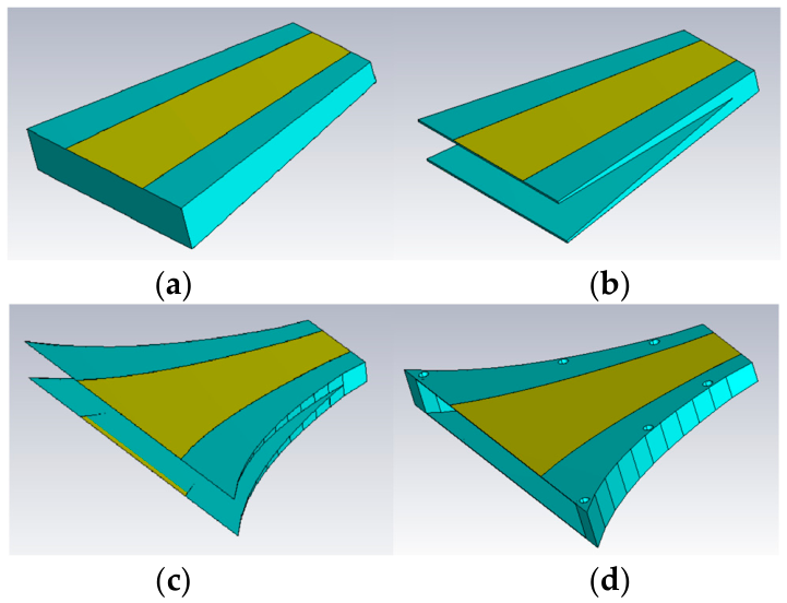
The first impedance transformer design (V1), which is a conventional parallel plate transmission line separated by a homogeneous dielectric, is not depicted in this paper for brevity. Moving forward, this paper only discusses and shows figures and results for design versions 2 and above. Version 2 (V2) of the PDT design establishes the baseline configuration featuring a solid polylactic acid (PLA) dielectric core with relative permittivity εr = 3.11 and top and bottom copper traces of 35 μm thickness. The V2 design demonstrated excellent performance in simulations, achieving reflection coefficient values below −15 dB across the 0.5–4 GHz frequency range. Figure 2a shows the initial impedance transformer design with 100% dielectric infill with identical copper traces on the top and bottom. The initial impedance transformer is then integrated with the combined antenna, as shown in Figure 1, represented by (6).
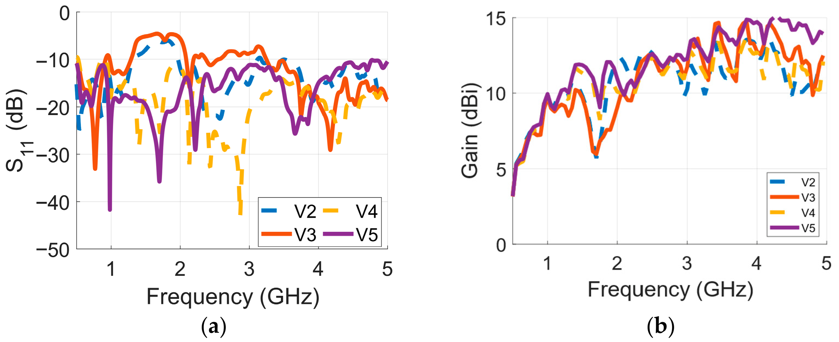
However, when integrated with the standalone combined antenna geometry, V2 revealed significant impedance mismatches at the dielectric-to-air transition region, particularly between 1–2 GHz, where S11 failed to meet the −10 dB threshold as illustrated in Figure 3a.
To address these interface discontinuities, version 3 (V3) introduced 45° wedge cuts along the dielectric edges, as shown in Figure 2b. These geometric modifications reduced impedance mismatches at very low frequencies while maintaining structural integrity. Subsequent electromagnetic simulations confirmed that V3 improved the matching at low frequencies but did not improve the overall bandwidth performance, though it introduced minor fabrication complexities due to its more intricate geometry.
In practice, once the PDT is integrated with the antenna, the environment seen by the transformer’s traces differs significantly from the isolated scenario. As the transformer’s top and bottom traces interface with the antenna’s flanges, the dielectric material between the traces abruptly transitions to free space in the antenna gap. The sharp dielectric-to-free-space gradient introduces reflections not captured in the isolated transformer simulations, ultimately influencing the overall antenna bandwidth and S11. To better prepare the transformer for realistic conditions, we alleviated the detrimental effects of the dielectric discontinuity and improved the performance of the integrated system. Therefore, the PDT was further improved by segmenting the transition dielectric as shown in Figure 2c,d, while maintaining a gradual material transition through the segments.
The design of the transformer involved maintaining a characteristic impedance (Z0) of 50 ohms and using a dielectric constant (εr) of 3.11 for PLA material. The calculation of the material and geometric properties was carried out as follows. The first 10 mm of the transformer is entirely PLA (100%), with dimensions provided in the first row of Table 1. This section is not graded and establishes the initial geometry. The remaining 70 mm of the transformer is divided into 10 graded cross-sections, each 7 mm apart. Ten sections were selected to limit fabrication complexity; using more sections would increase manufacturing difficulty. For each successive section, the volume percentage of the dielectric material is reduced by 10%, resulting in a gradual transition from 100% PLA to 0% PLA.
The transformer impedance at each cross-section was governed by two key equations. The effective permittivity and the characteristic impedance formula [20,21]:
ε r e f f = ε r + 1 2 + ε r 1 2 1 + 12 H W 1 2
Z 0 = 120 π ε r e f f [ W H + 1.393 + 0.667 l n ( W H + 1.444 ) ] 1
where H is the substrate height and W is the trace width.
Physically, reducing the effective permittivity along the transformer decreases the local wave slowdown and gradually transforms the fields from a dielectric-loaded region to an air-filled region. The corresponding trace-width adjustment maintains the target characteristic impedance, so the field distribution evolves smoothly instead of encountering an abrupt discontinuity. This graded transition reduces reflections at the transformer-to-antenna interface and improves wideband matching.
These equations precisely determined the dimensions for all ten graded sections of the PDT, as comprehensively detailed in Table 1. The table shows the complete transition from 100% PLA dielectric at the feed point to 0% dielectric material at the antenna interface, with the parameters of each section calculated to maintain proper impedance matching.
The height (H) of the transformer is determined by the constraints of the antenna. At the feed end (first cross-section), H = 7.7694 mm, based on the backplate slot height. At the transmitting end (final cross-section), H = 13.1549 mm, corresponding to the flange gap distance. The height changes linearly across the graded sections, with each step reducing the height by 10%.
The relative permittivity of each cross-section is calculated as follows [22]:
v =   ε r e f f 1 ε r 0 1  
where ε r 0 is the reference permittivity of the PLA material, and v represents the ratio of the effective permittivity to the baseline permittivity.
For each cross-section, the trace width (W) is computed using (1) and (2). Then the dielectric width is determined as twice the trace width (2W) for each cross-section to ensure proper impedance matching. Therefore, the permittivity and width of each section can be evaluated as shown in Table 1.
The 10% grading increment was selected as a practical compromise between electromagnetic smoothness and manufacturability. Finer segmentation can better approximate a continuous taper, but it also increases modeling, printing, alignment, and metallization complexity without producing a commensurate improvement in our design iterations. The linear height variation is dictated by the antenna geometry, namely the backplate slot at the feed end and the larger flange gap at the radiating end. Consequently, the dielectric-filling ratio and the cross-sectional height were co-varied to maintain a realizable 50-ohm transition.
The design evolution continued with Version 4 (V4), which implemented a carefully optimized tapered profile featuring ten distinct transition zones, as shown in Figure 2c. This iteration represented a significant advancement, achieving S11 below −12 dB across the 0.3–5 GHz target bandwidth, as shown in Figure 3. The tapered profile improved impedance matching and distributed the transition more gradually, which also improved mechanical robustness. The final iteration, Version 5 (V5), incorporated precision mounting interfaces, structural support ribs, and modified trace geometries to accommodate the N-type feed connector, as shown in Figure 1. Importantly, V5 retained the broadband matching advantages of V4 while solving practical integration challenges. The key graded-section dimensions are summarized in Table 1, and the updated figures include the principal dimensions required to reproduce the final design.
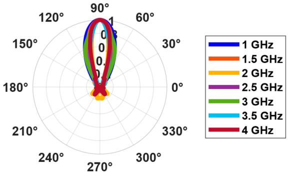
In addition, the simulated normalized radiation patterns of V5 are illustrated in Figure 4 at representative frequencies across the operating band, showing consistent directional radiation behavior. The gain increases with frequency because the antenna aperture becomes electrically larger in terms of wavelength, which improves aperture efficiency and directivity while the graded transition maintains acceptable matching. Accordingly, the highest simulated gain is 15 dBi near 2.1 GHz.
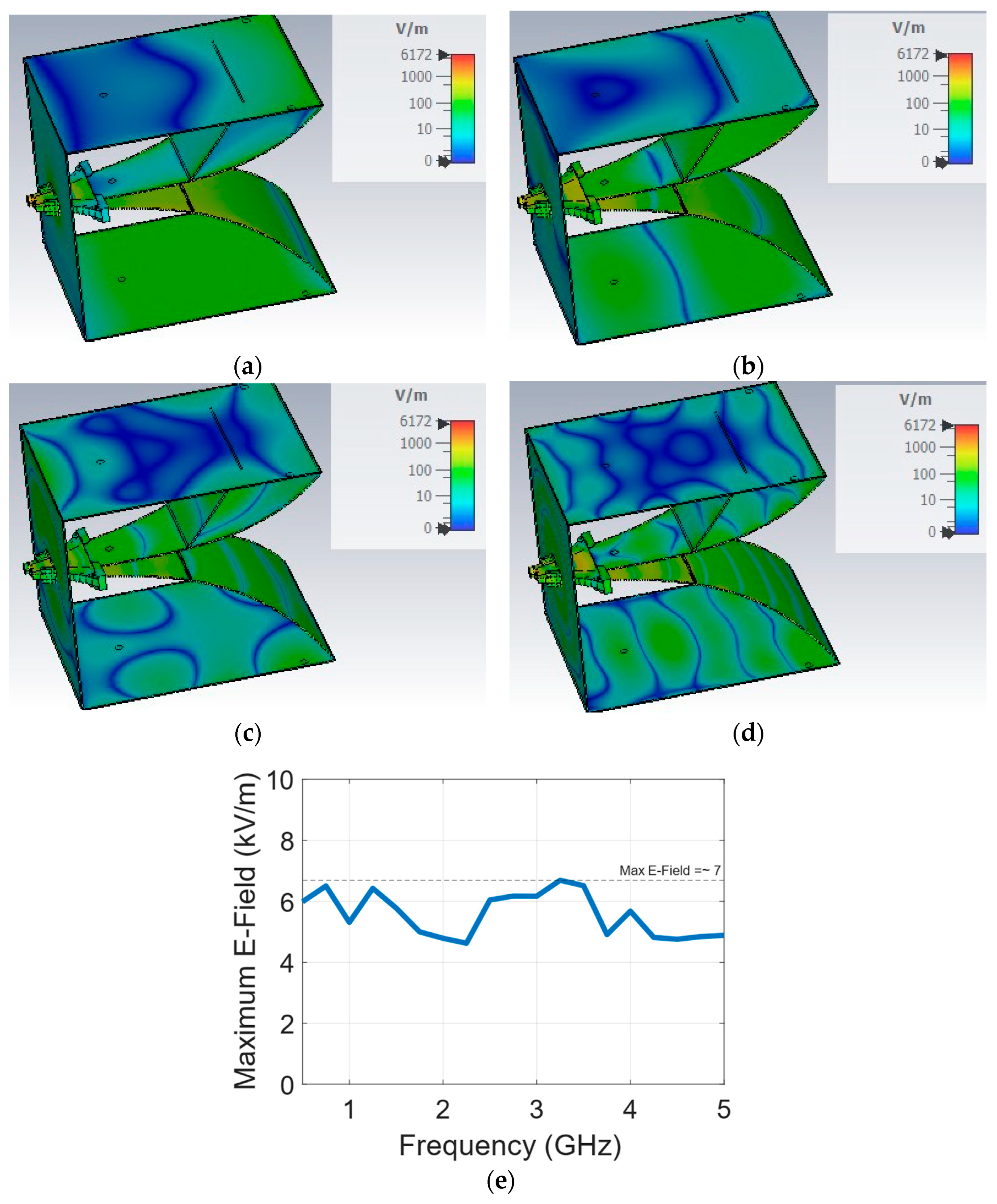
The proposed development process successfully addressed the fundamental challenges of broadband impedance matching in high-power UWB antennas while maintaining structural robustness for practical applications. Moreover, a theoretical estimate of the power-handling capability of the integrated PDT-antenna system can be obtained by examining the simulated 3D maximum electric-field distribution around the antenna, as illustrated in Figure 5. The highest local electric field in the V5 integrated model reaches approximately 7000 V/m when 0.5 W of input power is applied in the simulation. Because the electric field scales with the square root of the input power, the maximum peak power at which the adopted breakdown threshold (approximately 0.7 MV/cm) would be approached is [19]:
      p b r e a k d o w n =   E 1 E 2 2 × p i n
where E1 and E2 represent the adopted breakdown field and the maximum simulated electric field corresponding to the input power Pin, respectively. Hence, the final integrated system is estimated to tolerate approximately 50 MW peak power in simulation before approaching this threshold, thereby meeting the intended HPM design target.

3. Results

The antenna system, including PDT, was fabricated using additive manufacturing (AM) techniques to achieve precise geometric control while meeting structural and electromagnetic requirements. The antenna and PDT were 3D-printed using fused deposition modeling (FDM) with polylactic acid (PLA) as the primary dielectric material. The PLA was selected for its favorable dielectric properties (εr ≈ 3.11) and compatibility with high-resolution printing. The printing process was carefully controlled to maintain dimensional accuracy, with layer heights set to 0.1 mm for fine structural details.
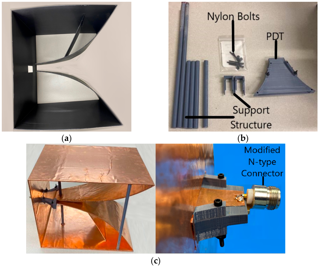
To ensure mechanical stability and electrical performance, the antenna frame was printed as a single integrated structure, eliminating assembly-related misalignments. Early prototypes (V2) used a two-part assembly for the antenna body, but this introduced unwanted seams that degraded RF performance. Subsequent iteration (V5) transitioned to a monolithic design, as shown in Figure 6a,b, significantly improving structural integrity and electromagnetic continuity.
After printing, the antenna’s conductive surfaces were metallized using adhesive-backed copper foil (35 μm thickness) to ensure low-loss RF performance, as shown in Figure 6c. The custom-modified connector was used to accommodate the changed feed geometry introduced by the PDT.
All measurements were conducted in an indoor laboratory environment to minimize external interference. A Rohde & Schwarz ZNA-43 vector network analyzer (VNA) was utilized for S-parameter characterization. The antenna was mounted on a non-conductive stand to reduce ground reflections, and the N-type feed was connected to the VNA through a low-loss coaxial cable for accurate S11 measurements.
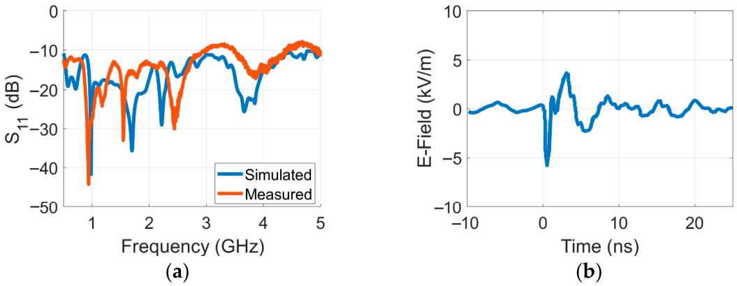
The final V5 prototype achieves a measured −10 dB reflection coefficient (S11) from 0.5 to 3.0 GHz, corresponding to an absolute bandwidth of 2.55 GHz and a fractional bandwidth of 148%. The fractional bandwidth is calculated as F B W   =   2 ( f _ H     f _ L ) / ( f _ H   +   f _ L )   × 100 % , where f _ L and f _ H are the lower and upper −10 dB cutoff frequencies of the continuous operating band. A second −10 dB operating band is observed from approximately 3.5 to 4.4 GHz, as illustrated in Figure 7a. This measured response aligns closely with simulation; the minor discrepancies above 3 GHz are attributed to fabrication tolerances and connector effects.
In addition, the antenna’s pulsed radiation capability was validated using a D-Dot sensor. The D-Dot sensor captures the radiated electric field in the time domain. For time-domain testing, the antenna was excited by a nanosecond-scale RF pulser, generating monopolar Gaussian pulses (~9–10 kV amplitude, 500 ps rise time). The D-Dot sensor, positioned 1 m from the antenna aperture, recorded the radiated field, which was subsequently integrated to derive the E-field waveform.
The raw sensor output was numerically integrated to derive the E-field waveform presented in Figure 7b, revealing a peak-to-peak amplitude of 10 kV/m at 1 m distance. Beyond the peak amplitude, the measured waveform preserves the intended monopolar character with limited trailing ringing, indicating that the PDT does not introduce severe pulse distortion within the validated operating regime. These results demonstrate the antenna’s ability to handle high-voltage pulses without breakdown in ambient conditions. A more comprehensive far-field pulse-fidelity study will be pursued once the anechoic chamber facility becomes operational.

4. Discussion

The proposed PDT-augmented combined antenna directly addresses this gap by delivering 148% fractional bandwidth, a simulated peak gain of 15 dBi, a simulation-based estimated power-handling capability of approximately 50 MW, and a total weight of only 197 g. When compared with the benchmarked works listed in Table 2, the advantages of our design become clear.
The combined antenna with Klopfenstein taper reported by Hao et al. [12] is notable for its outstanding power handling capability of 73 MW under 121 kV pulses, coupled with efficient broadband impedance matching. Nevertheless, its large 300 × 300 mm metallic aperture and heavy construction limit its suitability for size, weight, and power (SWaP)-constrained platforms such as UAVs or portable HPM systems. In contrast, our design achieves comparable wideband matching within a significantly smaller and lighter structure, reducing the mass by approximately 76%—while still sustaining multi-megawatt operation.
Chen et al. [18] demonstrated an all-metal antipodal Vivaldi antenna covering the 8.3–10.66 GHz range with a gain of 5.71 dBi, supported by an inherently high breakdown margin. While the electrical performance is impressive, the heavy, machined-metal construction increases cost and fabrication time. The PDT-augmented antenna reaches a simulated peak gain value of 15 dBi and maintains competitive wideband coverage, yet it is fabricated via additive manufacturing in lightweight PLA with copper metallization, offering significant advantages in cost, turnaround time, and portability.
The segmented TEM horn presented in [23] excels at high-dynamic-range calibration pulses in the 48–150 MHz range. Although effective for low-frequency applications, its operational band is too narrow for the multi-gigahertz demands of modern HPM systems. Our antenna, in contrast, spans 0.5–4.4 GHz in a single, compact element, combining wide bandwidth with robust high-voltage tolerance.
The 4 × 4 all-metal Vivaldi array reported in [24] delivers at least 9.5 dBi gain and can scale to higher power through arraying. However, it suffers from a narrower fractional bandwidth of around 80% and a large, heavy aperture. The proposed work not only achieves a higher simulated single-element peak gain of 15 dBi, but also offers approximately 85% broader bandwidth without requiring complex feed networks or array alignment, thereby improving deployment efficiency.
Similarly, the dual-podal multilayer Vivaldi array [25] achieves approximately 13 dBi gain across 8–12 GHz in a compact footprint, but it is designed for standard sensing power levels and lacks explicit high-power validation. The PDT-augmented antenna offers a higher simulated peak gain value while combining lightweight fabrication with a simulation-based estimated 50 MW power-handling capability that is supported qualitatively by the measured high-voltage pulsed tests.
Finally, the planar 2 × 4 horn array described by Semarak Ilmu [26] offers a high gain of 24 dBi and is capable of handling megawatt-class pulses. Nevertheless, its aperture exceeds 450 mm in size, and the heavy metallic structure limits portability. Our design offers a simulated peak gain value of 15 dBi, but with almost half the aperture size and at a fraction of the weight, allowing integration into mobile or airborne systems that cannot accommodate traditional horn arrays.
Overall, this comparison shows that while the existing literature demonstrates notable achievements in specific metrics, the proposed PDT-augmented combined antenna uniquely integrates ultrawide bandwidth, simulated high gain, high-voltage pulsed operation, low mass, and compact size within one platform for UWB high-power applications. These combined features make it particularly well-suited for next-generation applications where performance must be maximized without compromising portability or fabrication efficiency.
Although the graded PDT introduces additional geometric detail relative to a simple unfilled feed, the added complexity is primarily in the printed shape rather than in multi-part assembly. The antenna and transformer are still produced through a straightforward additive-manufacturing workflow followed by copper metallization. This tradeoff is favorable because the graded PDT substantially improves bandwidth and matching without resorting to bulky external transformers or heavy all-metal transition structures.
From a practical standpoint, the design is moderately sensitive to dimensional tolerances in the graded sections, copper-trace placement, and connector alignment, particularly above 3 GHz where the measured and simulated responses begin to diverge. Although a full statistical sensitivity analysis is beyond the scope of the present revision, this comparison indicates that the graded-section geometry, trace placement, and connector transition are the parameters most likely to influence the high-frequency response. The monolithic print reduces assembly errors, but printing resolution, dielectric inhomogeneity, and metallization seams can still perturb the local impedance. In addition, long-term environmental effects such as moisture absorption, temperature cycling, and adhesive aging of the copper foil may alter the dielectric and conductive properties over time. From an environmental perspective, additive manufacturing also reduces the need for repeated machined-metal prototype iterations, although durability and end-of-life handling of polymer-based structures remain important considerations. These factors motivate future tolerance and accelerated-aging studies.
The present single-element design can also serve as a building block for larger apertures or arrays. In that case, the graded PDT concept would remain applicable at each element feed; however, array implementation would additionally require careful control of element spacing, mutual coupling, feed-network power handling, and phase stability under pulsed excitation.
A current limitation of this work is the absence of complete anechoic-chamber far-field characterization of absolute gain, beamwidth, and pattern stability across the operating band. These far-field measurements will be reported in a future extended study.

5. Conclusions

In this study, we presented an ultrawideband combined antenna integrated with a graded partial dielectric transformer for high-power microwave applications. Through an iterative design and optimization process, we enhanced the antenna bandwidth while maintaining a compact form factor and strong high-voltage capability. The final prototype demonstrated a measured −10 dB reflection coefficient from 0.5 to 3.0 GHz, with an additional sub-band from 3.5 to 4.4 GHz, corresponding to a 148% fractional bandwidth. Simulations indicate a peak gain value of 15 dBi near 2.1 GHz, while time-domain measurements further validated the antenna’s ability to radiate high-voltage, short-duration pulses without breakdown in ambient air, reinforcing its suitability for practical HPM systems. A key innovation of this work is the use of additive manufacturing to fabricate the antenna structure from PLA with copper-foil metallization, resulting in a lightweight (197 g) yet robust design. Full far-field gain validation will be reported once the new anechoic chamber becomes operational.

Author Contributions

Conceptualization, methodology, formal analysis, and investigation, K.C.D.; software and validation, A.D.D.; writing, review and editing, M.Z.M.H. All authors have read and agreed to the published version of the manuscript.

Funding

This work was partially funded by the Office of Naval Research (ONR) under grant number N00014-17-1-3016. The views expressed are those of the authors and do not reflect the official policy or position of the Department of Defense or the U.S. Government.

Data Availability Statement

The original contributions presented in this study are included in the article. Further inquiries can be directed to the corresponding author.

Conflicts of Interest

The authors declare no conflicts of interest.

Abbreviations

The following abbreviations are used in this manuscript:
HPMHigh-power microwave
UWBUltrawideband
SWaPSize, weight, and power
PDTPartial dielectric transformer
VSWRVoltage standing-wave ratio
PLAPolylactic acid
VNAVector network analyzer

References

  1. Min, S.-H.; Jung, H.; Kwon, O.; Sattorov, M.; Kim, S.; Park, S.-H.; Hong, D.; Kim, S.; Park, C.; Hong, B.H.; et al. Analysis of Electromagnetic Pulse Effects Under High-Power Microwave Sources. IEEE Access 2021, 9, 136775–136791. [Google Scholar] [CrossRef]
  2. Sun, Y.; Dang, F.; Yuan, C.; He, J.; Zhang, Q.; Zhao, X. A Beam-Steerable Lens Antenna for Ku-Band High-Power Microwave Application. IEEE Trans. Antennas Propag. 2020, 68, 7580–7583. [Google Scholar] [CrossRef]
  3. Hamdalla, M.Z.M.; Zawad, M.; Kunkle, M.; Baidya, S.; Allen, R.C.; Bland, P.J.; Fields, T.D.; Hassan, A.M. Design of a 3D Printed Wide Band Metasurface Antenna for High Power Applications. Prog. Electromagn. Res. M 2024, 128, 115–125. [Google Scholar] [CrossRef]
  4. Benford, J.; Swegle, J.A.; Schamiloglu, E. High Power Microwaves, 3rd ed.; CRC Press: Boca Raton, FL, USA, 2015. [Google Scholar] [CrossRef]
  5. Zawad, M.; Rana, S.; Fields, T.D.; Caruso, A.N.; Durbhakula, K.C.; Hamdalla, M.Z.M. High-Power Microwave Antennas: A Comprehensive Review. IEEE Access 2025, 13, 76217–76256. [Google Scholar] [CrossRef]
  6. Doma, R.S.; Azeemuddin, S. A comprehensive review of high voltage wideband and ultra-wide band antennas for IEMI applications. Eng. Res. Express 2021, 3, 012001. [Google Scholar] [CrossRef]
  7. Koshelev, V.; Buyanov, Y.; Andreev, Y.; Plisko, V.; Sukhushin, K. Ultrawideband radiators of high-power pulses. In Proceedings of the PPPS-2001 Pulsed Power Plasma Science 2001. 28th IEEE International Conference on Plasma Science and 13th IEEE International Pulsed Power Conference. Digest of Papers (Cat. No.01CH37251), Las Vegas, NV, USA, 17–22 June 2001; Volume 2, pp. 1661–1664. [Google Scholar] [CrossRef]
  8. Balzovsky, E.; Buyanov, Y.; Koshelev, V.; Nekrasov, E. Compact combined antenna for high-power ultrawideband radiation sources with subnanosecond pulse duration. Microw. Opt. Technol. Lett. 2021, 63, 2866–2869. [Google Scholar] [CrossRef]
  9. Lenzing, E.H.; Pastore, R.A.; Hechtman, C.D.; Lenzing, H.E.; Kunhardt, E.E. Ultra-Wideband Antenna for High-Power Operation. In Ultra-Wideband, Short-Pulse Electromagnetics 2; Carin, L., Felsen, L.B., Eds.; Springer: Boston, MA, USA, 1995; pp. 209–214. [Google Scholar] [CrossRef]
  10. Choi, J.-Y.; Ma, J.-S.; Kim, W.-S. Reconfigurable Wideband Bandpass Filter Using Stepped Impedance Resonator Based on Liquid Crystals. Electronics 2025, 14, 2325. [Google Scholar] [CrossRef]
  11. Gao, Z.; Sun, L.; Zhan, J.; Nian, F. Design and Simulation of Broadband Impedance Transformer Based on Stepped Impedance Transform Line. In Proceedings of the 2022 International Conference on Microwave and Millimeter Wave Technology (ICMMT), Harbin, China, 12–15 August 2022; pp. 1–3. [Google Scholar] [CrossRef]
  12. Wu, H.; Qu, J.; Chen, S.; Yu, C.; Liu, L.; Shi, X. Design and experiment of ultra-wideband combined antenna for high-power microwave. High Power Laser Part. Beams 2023, 35, 073001-6. [Google Scholar] [CrossRef]
  13. Wang, S.-F.; Xie, Y.-Z. Design and Optimization of High-Power UWB Combined Antenna Based on Klopfenstein Impedance Tape. IEEE Trans. Antennas Propag. 2017, 65, 6960–6967. [Google Scholar] [CrossRef]
  14. Hsieh, S.-N.; Chang, S.-L.; Chen, C.-J. A Dual-Band Quarter-Wave Transform and Its Applications to Directional Coupler Design. Electronics 2025, 14, 2881. [Google Scholar] [CrossRef]
  15. Kittiwittayapong, S.; Torrungrueng, D.; Phaebua, K.; Lertwiriyaprapa, T.; Akkaraekthalin, P.; Sukprecha, K. Wideband Impedance Matching Using Quarter-Wave-Like-Transformers Implemented by Asymmetric Compact Microstrip Resonant Cells. In Proceedings of the 2021 Research, Invention, and Innovation Congress: Innovation Electricals and Electronics (RI2C), Bangkok, Thailand, 1–3 September 2021; pp. 149–153. [Google Scholar] [CrossRef]
  16. Kumar, O.P.; Kumar, P.; Ali, T.; Kumar, P.; Vincent, S. Ultrawideband Antennas: Growth and Evolution. Micromachines 2022, 13, 60. [Google Scholar] [CrossRef] [PubMed]
  17. Nikolaou, S.; Quddious, A.; Nikolaou, S.; Quddious, A. Antennas for UWB Applications. In UWB Technology—Circuits and Systems; IntechOpen: London, UK, 2019. [Google Scholar] [CrossRef]
  18. Chen, Z.; Yin, R.; Jiang, Y.; Mao, X.; Lv, P.; Jiang, S.; Liu, Y. An All-metal Antipodal Vivaldi Antenna Design for High-power Microwave Application. Appl. Comput. Electromagn. Soc. J. ACES 2024, 39, 1066–1072. [Google Scholar] [CrossRef]
  19. Yadav, S.V.; Chittora, A. A compact ultra-wideband transverse electromagnetic mode horn antenna for high power microwave applications. Microw. Opt. Technol. Lett. 2021, 63, 264–270. [Google Scholar] [CrossRef]
  20. Pozar, D.M. Microwave Engineering, 4th ed.; Wiley: Hoboken, NJ, USA, 2012; Available online: https://www.wiley.com/en-us/Microwave+Engineering%2C+4th+Edition-p-9781118213636 (accessed on 26 April 2024).
  21. Balanis, C.A. Antenna Theory: Analysis and Design, 4th ed.; Wiley: Hoboken, NJ, USA, 2016; Available online: https://www.wiley.com/en-us/Antenna+Theory%3A+Analysis+and+Design%2C+4th+Edition-p-9781118642061 (accessed on 8 August 2025).
  22. Zhang, S.; Arya, R.K.; Pandey, S.; Vardaxoglou, Y.; Whittow, W.; Mittra, R. 3D-printed planar graded index lenses. IET Microw. Antennas Propag. 2016, 10, 1411–1419. [Google Scholar] [CrossRef]
  23. Zhang, T.; Wei, Y.; Wang, Y.; Duan, C.; Wang, L.; Li, Z.; Li, X.; Li, X.; Cao, B. Design of Segmented Ultra-Wideband TEM Horn Antenna for Calibration of Wideband Electromagnetic Pulse Sensors. Sensors 2025, 25, 3599. [Google Scholar] [CrossRef] [PubMed]
  24. Lim, T.H.; Park, S.; Lee, C.-S.; Park, J.R.; Choo, H. Design of an All-Metal Vivaldi Array Antenna with Dual-Slant Polarization for High-Power Jammer Systems. J. Electromagn. Eng. Sci. 2024, 24, 393–400. [Google Scholar] [CrossRef]
  25. Nasir, M.; Iftikhar, A.; Shafique, M.F.; Saka, B.; Nikolaou, S.; Anagnostou, D.E. Broadband dual-podal multilayer Vivaldi antenna array for remote sensing applications. IET Microw. Antennas Propag. 2023, 17, 505–517. [Google Scholar] [CrossRef]
  26. Miligy, A.F.; Taher, F.; Elwi, T.A.; Abdelaleim, M.; Sree, M.F.A.; Fatah, S.Y.A. Broad Band 2×4 Horn Antenna Array for High Power Microwave (HPM) Systems Application. J. Adv. Res. Appl. Sci. Eng. Technol. 2026, 64, 1–17. [Google Scholar] [CrossRef]
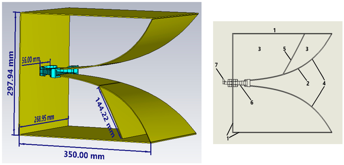
Figure 1. Combined antenna with the integrated PDT at the feed region with all the dimensions included. The figure notations are: (1) body; (2) electrical monopole; (3) magnetic dipoles; (4) TEM horn; (5) plate; (6) dielectric transformer; and (7) modified 50 Ω N-type feed.
Telecom 07 00054 g001
Figure 2. Evolution of PDT prototypes: (a) V2: Solid dielectric, (b) V3: Wedge-cut design, (c) V4: Optimized taper, (d) V5: Final integrated version. Dimensions in millimeters.
Telecom 07 00054 g002
Figure 3. (a) Simulated S11 and (b) gain for prototypes V2–V5 integrated with the combined antenna.
Telecom 07 00054 g003
Figure 4. V5 antenna normalized radiation pattern.
Telecom 07 00054 g004
Figure 5. Field distribution around the antenna at (a) 0.5 GHz. (b) 1 GHz. (c) 2 GHz. (d) 3 GHz. (e) The maximum value across the frequency range.
Telecom 07 00054 g005
Figure 6. (a) Preprocessed antenna frame printed as a single integrated assembly and (b) PDT V5 combined antenna support structure and PDT, highlighting the internal printed framework. (c) Combined antenna with integrated PDT, post-metallization and overall assembly and modified N-type connector side view.
Telecom 07 00054 g006
Figure 7. (a) Comparison between the measured and simulated S11 of the combined antenna with integrated PDT, (b) Measured E-field vs. time at 1 m.
Telecom 07 00054 g007
Table 1. Material and Geometric Properties.
εreffVolume %ε0, PLALength from Feed (mm)Dielectric
Outer (mm)
Dielectric
Inner (mm)
Trace Outer (mm)
HeightWidthHeightWidthHeightWidth
3.11000100%3.1110.07.769438.447.769438.447.769419.22
2.8990090%3.1117.08.307943.127.477143.128.307921.56
2.6880080%3.1124.08.846548.297.077248.298.846524.145
2.4770070%3.1131.09.385054.066.569554.069.385027.03
2.2660060%3.1138.09.923660.525.954160.529.923630.26
2.0550050%3.1145.010.462167.865.231167.8610.462133.93
1.8440040%3.1152.011.000776.284.400376.2811.000738.14
1.6330030%3.1159.011.539286.063.461886.0611.539243.03
1.4220020%3.1166.012.077897.642.415697.6412.077848.82
1.2110010%3.1173.012.6163111.71.2616111.712.616355.85
1.000000%3.1180.013.1549129.280.0000129.2813.154964.64
Table 2. Comparison with Recent High-Power Antennas Matching Performance.
Ref.Frequency RangeGain (dBi)Aperture/Size (mm)Power Handling/NotationFabrication/Notes
[12]UWB~6–9 ~300 × 300~73 MW (121 kV pulses, 329 MHz)Metallic; integrated Klopfenstein taper
[18]8.3–10.66 GHz~5.71~35 × 358000 W CWMachined sheet metal (all-metal)
[23]48 MHz–150 MHz10.9~1000–1000High dynamic range calibration pulses3D-printed support + metal radiators
[24]2–6 GHzSingle element: ~8–12; array: ≥9.5Aperture few hundred mmScalable to HPMMachined all-metal array
[25]5.5–20.82 GHzSingle element: 9.33; array: 1329 × 21Standard remote-sensing powerMultilayer PCB feed
[26]8–12 GHz~24457.2 × 457.2MW-class pulses (sim/exp)Machined metal array
This Work0.5–4.4 GHz15297 × 25950 MW3D-printed PLA + copper foil
Disclaimer/Publisher’s Note: The statements, opinions and data contained in all publications are solely those of the individual author(s) and contributor(s) and not of MDPI and/or the editor(s). MDPI and/or the editor(s) disclaim responsibility for any injury to people or property resulting from any ideas, methods, instructions or products referred to in the content.