


Abstract
The inkjet printing technique has been rapidly developing for the realization of flexible electronic devices. The antennas, sensors and transistors have been successfully introduced on flexible substrates such as glass, silicone and many films. Since the inkjet printing technique is a direct writing process, the benefits include flexible design, low-cost and environmentally friendly. It is also possible to create a high resolution of printed lines. Therefore, this technique is believed to have a great potential for applying on textile substrates. However, the challenge is to ensure that the small droplets can penetrate through the thickness of the fabric in order to spread along the threads. Thus, the uniformity and continuity are not acceptable for practical applications. This paper summarises inkjet printing technologies and potential applications on textile substrates.
1. Introduction
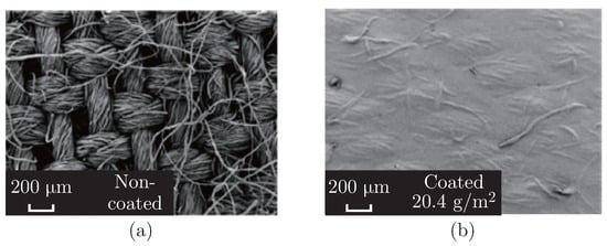
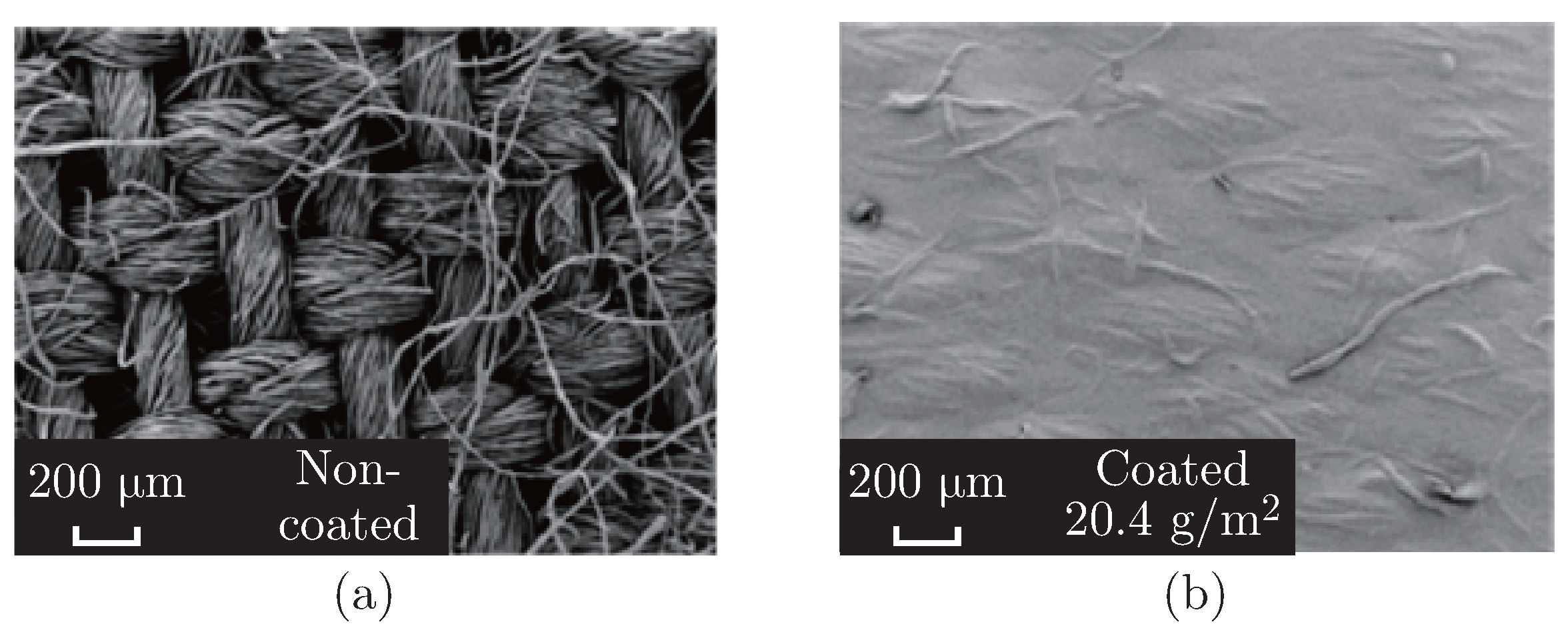
E-textiles are defined as textiles that enable electronic components such as sensors, batteries, light, chips and small computers and electronic circuits to be embedded and built from fibres and textile structures. E-textile is designed to sense, react with, and adapt to external conditions or stimuli in a manual or programmed manner [1]. An important target is to achieve conductive property. Traditionally, textile-based wearable devices are manufactured through weaving, knitting, sewing and embroidering conductive threads inside non-conductive substrates. Traditional technologies face limitations such as difficulty in obtaining a homogeneous line width and gap [2] and the significant skin effect that occurs at high frequency [3]. Hence, inkjet printing technology is a promising method to provide thin conductive films with very high resolution. The inkjet printed line and space dimensions can be as small as 10-20 µm, which is at least one-fifth of a screen printed line [4]. At present, this technique has formed conductive tracks on the smooth, homogeneous, impermeable and non-deformable substrates like paper [5], PET [6], PDMS [7], Kapton [8] films. Although the inkjet printing technology provides an ideal approach to produce entire electronic circuits, the textile substrate itself hinders the development. The rough and porous surface results in a discontinuous track with low resolution because the droplet penetrates through the thickness of fabric and then spreads along the yarns [9]. The typical solution to overcome the roughness and porosity is coating a hydrophobic interface layer. As shown in Figure 1, the crimps and gaps between fibres and yarns are filled after coating. The average thickness of the interface layer is around 100 µm with a surface roughness of 5 µm [10]. This paper reviews the inkjet printing techniques and discusses the potential applications on textile substrates.
Figure 1.
Comparisons of (a) non-coated and (b) coated fabrics [11] Copyright© 2017 American Chemical Society.
2. Inkjet Printing Techniques
Before the development of inkjet printing, printing technologies such as gravure, flexography, lithography and screen printing have been used to print inks on textile substrates. The conventional graphics printing produces images made up of isolated drops, while the functional materials printing require the drops to overlap to form lines or continuous areas from the overlap of lines [12]. Table 1 compares the advantages and disadvantages of various printing technologies. The inkjet printing technology has bright future because it only needs to follow a pre-designed computer layout and directly creates a pattern without utilising masks. The inkjet printing technique is divided into direct printing or indirect transfer printing. In general, the direct printing process deposits conductive inks on the desired substrate, while the transfer printing process firstly prints on a transfer paper then heat transfers to the desired substrates [13]. The limitation of transfer printing technique is only suitable for the heat resistance polymers, while the direct printing process has no restriction to substrates [14].
Table 1.
Comparisons of various printing technologies [15].
2.1. Printable Inks
The printable ink has wide range of choices such as conductive, semi-conductive, and physical inks. Usually, the conductive inks are separated into metal nanoparticle inks, organometallic inks, conductive polymers, graphene ink and carbon nanotubes ink [16]. The metal nanoparticle ink is an excellent choice due to the high surface area to volume ratio. Hence, metal nanoparticle inks get unique properties including electronic, magnetic, optic, catalytic, and thermodynamic [17]. Among various metals, gold is too expensive for mass production of gold nanoparticles. The copper nanoparticle ink is cheap and easy to disperse into water, but the printed track has low electrical due to poor oxidation resistance [18]. The silver nanoparticle ink is considered as the optimum because of high electrical conductivity and good resistance to oxidation. Besides, the attractive conductive polymers are polyaniline (PANI), polypyrrole (PPy) and poly(3,4-ethylenedioxythiophene) (PEDOT) [19]. As investigated, these polymers have high electrical conductivity and environmental stability, but poor mechanical properties. Moreover, the graphene inks have potentials in the field of printed electronics good electrical, optical, and mechanical properties [20], so it is an alternative to metal nanoparticles. On the other hand, the transition metal dichalcogenides (TMDs) such as MoS2, WS2 and MoSe2 and black phosphorus have shown semi-conductive character [21]. These kinds of materials require a sizeable bandgap, a high carrier mobility and ION/IOFF > 104 to achieve logic electronic applications.
The inkjet printability (Z) is an important factor to predict the droplet formation. Z value stems from Reynolds (Re), Weber (We) and Ohnesorge (Oh) numbers (see Equation (1)) [22,23]. A Z value from 1 to 10 is suitable for stable drop formation. The droplets would be the satellite if over 10, while the ink is too viscous if below 1 [24]. As recommended, the viscosity should be within the range of 1-25 mPa·s, and the surface tension would be between 25 and 50 mNm−1 [16].
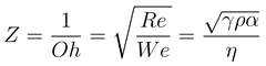 where ν, α, ρ, η and γ represent the velocity, drop diameter, density, viscosity and surface tension of the ink, respectively.
Table 2.
Comparison between CIJ and DOD printer [24], [25].
2.2. The Working Mechanism of the Inkjet Printer
There are two basic categories of inkjet printing machines, which are the continuous inkjet (CIJ) printer and the drop on demand inkjet (DOD) printer. In CIJ printing, a force is applied to a liquid jet to induce the stream to break up into a series of droplets of uniform size and spacing. Unwanted drops are deflected by an external electrical field to control the drop position [24]. In some situations, the unused ink is recycled so that it might contaminate the original ink. On the other hand, the DOD printer only forms and ejects droplet where required via controlling heat or voltage [16]. Table 2 compares these two printers. The DOD printer is a more economical and flexible setup to print high-resolution pattern due to ejecting the smaller droplet and the better control of the deposited position. The DOD printer applies both thermal and piezoelectric techniques to form droplets. For the thermal ink jet, a heater quickly raises the temperature of the ink over 300 °C, which causes a vapour bubble to eject a droplet [26]. For the piezoelectric ink jet, an electrical signal is applied to suddenly change the volume of piezoelectric material, which generates a pressure pulse in the fluid and forms a droplet [16]. The researchers prefer piezoelectric inkjet printer because it is a relatively easy method to control drop size and velocity for any fluid [24]. After forming a drop, the droplet breaks away from the nozzle if the kinetic energy imparted by the pressure wave is sufficient to overcome viscosity itself and the surface tension keeping it attached to the nozzle [16,27]. After the droplet leaves the nozzle, the liquid breaks up into two parts, a primary drop and a satellite. In some cases, the satellite merges with the primary drop, or it travels alone. To prevent additional drops or satellites, the pulse shape parameters, such as the pulse amplitude and the dwell times, should be carefully modified [28]. During the flight, the velocity of the droplet must be several metres per second to overcome drag due to air.
2.3. Drop Spreading on Smooth and Rough Substrate Surfaces
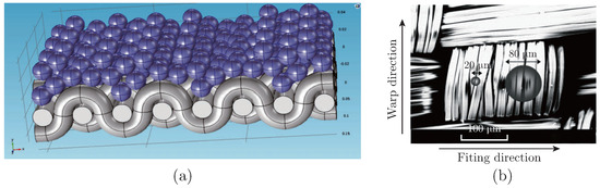
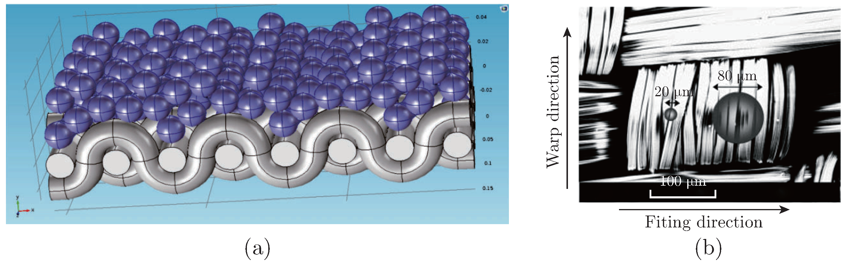
The interaction between liquid and substrates directly determines the resolution. The substrates can be separated into smooth and porous surfaces. The interaction on flat surfaces like PET and Kapton film is divided into two stages. Firstly, when the droplet hits the substrate, the kinetic energy of the impact is partially dissipated by viscous forces. After that, the rest of energy is converted to spread the droplets to a diameter determined by the relative surface energy between the ink and the substrate [16]. Therefore, the drop spreading is affected by several factors including drop speed, drop volume, liquid physical properties, solid surface energy, drop/surface interaction, and surface characteristics [29]. In the field of conductive ink, the contact angle is a good indication of interaction but is not sufficient for predicting the electrical resistance [30]. In general, the thin line width can be obtained by printing on a high contact angle substrate [3], but the electrical resistance might be influenced by the ink de-wetting, cracking phenomenon and residual thermal stresses [31,32]. Unlike those substrates with the smooth surface, the fabrics are rough and porous. A simple model is built to predict the interaction to investigate the relationship between fabric topography and deposited droplet [33]. The woven fabric model is first constructed, and then fine mesh is made to simulate the silver particles (see Figure 2(a)). This process assumes the silver particle diameter is the same as yarn diameter and ignores the gaps between yarns. However, these assumptions would not happen in real life. As seen from Figure 2(b), the ejecting droplets (∼20 and ∼80 µm) are much smaller than the width of single yarn (250 µm) [29]. Therefore, the inks would easily penetrate through the thickness of fabric, then spread along the threads.
Figure 2.
(a) Model of the silver particles deposition on woven fabric [33] Copyright © 2018 by SAGE Publications; (b) A SEM photograph of actual droplets on fabric [29] Copyright © 2006 Woodhead Publishing Limited.
Up to now, there are not many investigations in the field of inkjet print conductive inks on untreated fabrics. Only Karaguzel researched on inkjet print a purple dye (a mixture of glycerol, water, and 4% acid red) on nonwoven fabrics [34]. The droplet spreads and forms a film between the neighbouring hydrophilic fibres. When the capillary space is small, the deposited droplet takes the form of a film or liquid bridge between several fibres depending on the wetting behaviour of the liquid. In another research field, the wetting behaviour of water inside fabrics is well investigated [9]. The study of water transport could be a reference to the conductive ink spreading inside textiles. When the water drop impacts on textile substrates, the wetting mechanisms such as spreading, immersion, adhesion and capillary penetration may operate simultaneously [35]. The hitting process comprises two steps: the dynamic spreading first occurs very rapidly, and the penetration on porous substrates can result in further spreading. The dominant physical mechanisms during spreading are kinetic and surface energies, while that during penetration is capillary force [29].
The yarn or fabric wettability is mostly determined by the yarn construction features such as twist, diameter, crimp, and fibre denier rather than the fibre wettability [36]. The dominant physical mechanisms during interaction are the capillary pressure force, which is exerted by the airspace within the yarn, referred to as inter-fibre pores. The capillary force drives liquid through the yarn or fabric. A simple model is created by Hollies and his colleges [37] to relate the vertical capillary distance with capillary space,
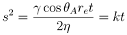
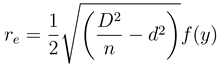 where s is a horizontal distance travelled, θA is the advancing contact angle, re is capillaries of effective radius calculated by Equation (3), k is the water transport rate, t is time, D is circular yarns of diameter, n is number of fibres, d is circular fibre diameter and f(y) is a continuity and distribution function for capillaries in a real yarn. This model is good to predict the vertical wicking length of water or ink. As seen from Equation (2), the more capillary space leads to the longer wicking distance and larger wicking rate for the same yarn and liquid. In case of predicting the covered area of the fabric, the liquid properties, drop volume and wicking time are important parameters [38]. The effective porosity ϕ∗ is still suitable to predict drop spreading [39]. In case that the ink fully penetrated through the thickness of all the fabrics, the spreading area Ad can be calculated,
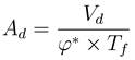 where Vd is the drop volume in cm3, Tf is fabric thickness in cm, and ϕ∗ is effective porosity, which is a combined measure of porosity, wettability, distribution, and continuity of capillaries. As seen from Equation (4), the higher porosity leads to the penetration of liquid through the thickness of fabrics that result in the smaller drop spreading area for the same fabric and liquid volume. To sum up, the porosity is a significant parameter for drop spreading on both yarns and fabrics (see Equation (2) and (4)). No matter what types of textile fabrication methods provides structures with high surface roughness and porosity, so the edge of the printed line is blurry and bleeding. Complicatedly, the contact angle of some high permeable fabric surfaces is almost zero, which means the conductive ink is all absorbed by the yarns. In this case, so the conductivity of wicked silver track is also low because the continuity of capillaries formed by the fibres of the yarn is low [37].
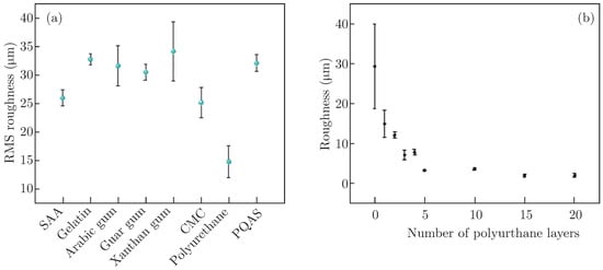
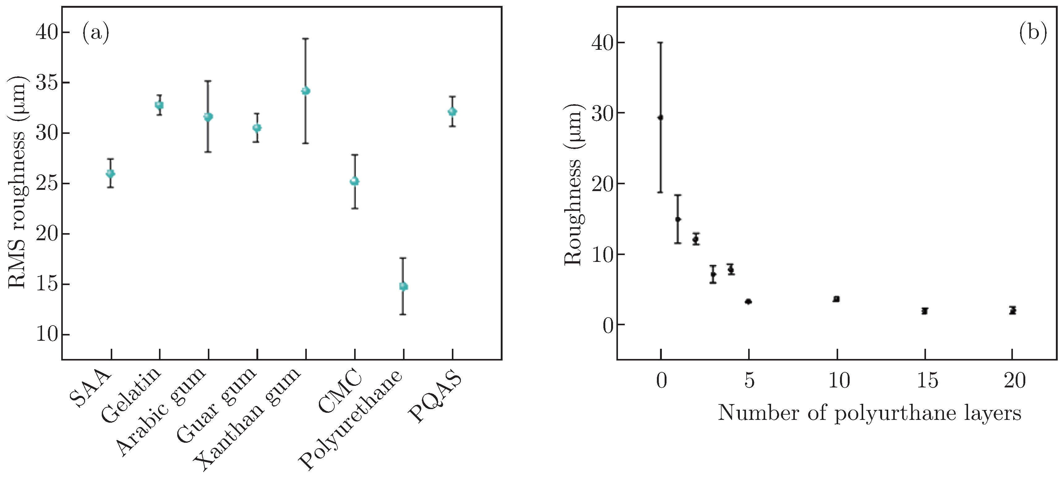
Based on these findings, some solutions are developed to overcome the roughness and porosity (see Table 3). Coating an interface layer provides a smooth and impermeable surface, which is similar to flexible film. Most researchers prefer the UV-curable screen printable ink since it is a cheap and commercial product. As reported, the surface roughness of the UV-curable polyurethane acrylate based interface layer on 65%/35% polyester/cotton fabric was less than 5 µm [40], which is smooth enough to achieve narrow and high-resolution line. A few years later, a smoother surface (∼1.5 nm) is produced by Krykpayev and his college [41] on the same fabric. Apart from polyurethane, sodium alga acid (SAA), gelatin, arabic gum, guar gum, xanthan gum, sodium carboxymethylcellulose (CMC), polymerizable quaternary ammonium salt (PQAS) have been tried in Carey and his colleagues’ experiments. After measuring the roughness by Profilometer, the polyurethane is proven as the smoothest interface [42] (see Figure 3). Some other materials like cellulose nanofibrils (CNFs) [11] and polyvinyl alcohol [18,43,44,45] are also applied. Similarly, some resins [46,47] are introduced to fill the hole and provide a relatively smooth surface. In conclusion, the conductivity of silver printed pattern on the coated interface layer varies from 104 to 106 S/m, which is considered as acceptable when compared with most conductive threads. However, the drawback of coating a layer is non-compatible between various layer and inks, which leads to the de-wetting phenomenon [48]. For the UV-curable ink, thermal and UV-ozone posttreatments should follow the inkjet printing process to solve the de-wetting of silver inks on the interface layer [30]. Besides, an inkjet printed hydrophobic nanoparticle layer on yarns is suggested to achieve low resistance silver and graphene pattern on cotton/polyester fabrics when compared with samples without coating. Overall, the coating technique significantly changes the physical and chemical properties of laminated fabrics, so this technique still needs to promote.
Figure 3.
(a) Roughness of the various planarization layers (b) Polyurethane planarization layer as a function of coating passes ©2018 Springer Nature Limited [42].
On the other hand, the electroless plating technique helps to form conductive patterns on textiles. The process is firstly inkjet printing a seed layer like palladium or silver particles on fabrics, and then dipping the fabric inside an electroless plating bath until the copper or nickel particles are subsequently deposited on the seed layer [49]. This approach avoids the influence of porous structure, but it is difficult to achieve high resolution of the printed line. The plasma surface treatment is mentioned to improve the resolution, pattern sharpness, anti-bleeding and adhesion [50,51]. The plasma treatment is applied in the electroless plating process to increase the hydrophilicity of mould surface [52]. Besides, the oxygen plasma dramatically improves the print quality of conductive polymer patterns on ITO (indium tin oxide) films [53] and silver nanoparticles patterns on PET films [51]. In sum, breakthroughs are still required in the field of inkjet printing conductive inks on textiles.
2.4. Sintering Process
After the deposition of the conductive ink, sintering process is an important step to improve conductivity. Since most metal nanoparticles are dissolved into the organic solvent, the rapid evaporation is required to increase the contact points between distributed nanoparticles [4]. For the silver nanoparticles, the conductivity rises sharply when the temperature changes from 100 °C to 150 °C. Then the conductivity keeps relatively steady over 150 °C [54]. However, extended exposure to high temperature results in a gradual decomposing to fabrics [55]. Therefore, the reactive inks are succeeded to dry printed patterns at room temperature [56]. Similarly, the drying temperature of sequential printing of GO ink and the ink containing a reducing agent can be lowered to 60 °C [57]. Moreover, choosing a solvent with no binder might be another trend to protect fabrics [58].
Table 3.
Lists of existed solutions to inkjet print conductive inks on textile [15].
3. Applications of Inkjet Printing Technology
As discussed above, textiles are still not considered as an inkjet printable substrate. Therefore, most wearable applications have been realized on paper substrates or flexible films like Polyurethane (PU), Polydimethylsiloxane (PDMS) and Polyethylene terephthalate (PET). This chapter would discuss some interesting inkjet-printed devices on films and textiles. Depending on the types of ink, the applications include conducting, semiconducting, and physical. The conductive inks mainly form circuits, electrodes, OLEDs, and some resistance based sensors. The semi-conductive inks are used to print (opto) electronics like photodetectors and transistors. Besides, many 2D materials show excellent mechanical strength, thermal and chemical stabilities, so they have been considered in a variety of barrier, membrane and filtration [21].
3.1. Conductive Inks
Metal nanoparticle inks like silver and copper are commercial products to date. Graphene and related 2D material inks are considered as alternative products. Some conductive polymer inks like PEDOT:PSS are reported to increase the flexibility of printed patterns. The electrical contacts and circuits are normally fabricated by inkjet printing these conductive inks. Silver [42] and PEDOT:PSS [62] electrodes have been printed to act as source, drain and gate and form the field effect transistor (FET). Besides, the antenna is an important application. Traditional wearable antennas are mounted on the rigid PCB, which limits the development of wearable devices. The flexible films and textile substrates support the excellent flexibility and comfort. Table 4 illustrates two inkjet printed antennas on polyester/Cotton fabrics and on the PET film. The textile antenna performances are acceptable for particular applications such as localization circuit [41]. However, the gain and efficiency of textile antenna is not good as those printed on the PET film.
Table 4.
Inkjet printed antennas [15].
3.2. Inkjet Printed Sensors
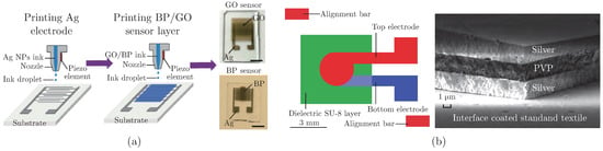
Sensors are a major application field for the inkjet printing technology. They include chemical, strain, pressure and touch sensors. The chemical sensors rely on the ink properties. Take the graphene as an example, the functionalisation of graphene with groups such as =O, -NH2, -OH, -F, -CH3 and –SO3H expand its sensing capabilities to a wide range of chemicals, including NO, NO2, Cl2, SO2, CHCl3, CH3OH and C6H14 [21]. Besides, the black phosphorus are reported to have 20 times higher sensitivity and 40 times faster response time than graphene and MoS2 [63]. A humidity sensor is fabricated by print graphene oxide and few-layered black phosphorus flakes as sensing layer on the glass substrate (see Figure 4(a)). The sensor reveals a high capacitance sensitivity of 4.45 × 10⁴ times for the GO sensor and 5.08 × 10³ times for the BP sensor [64].
Figure 4.
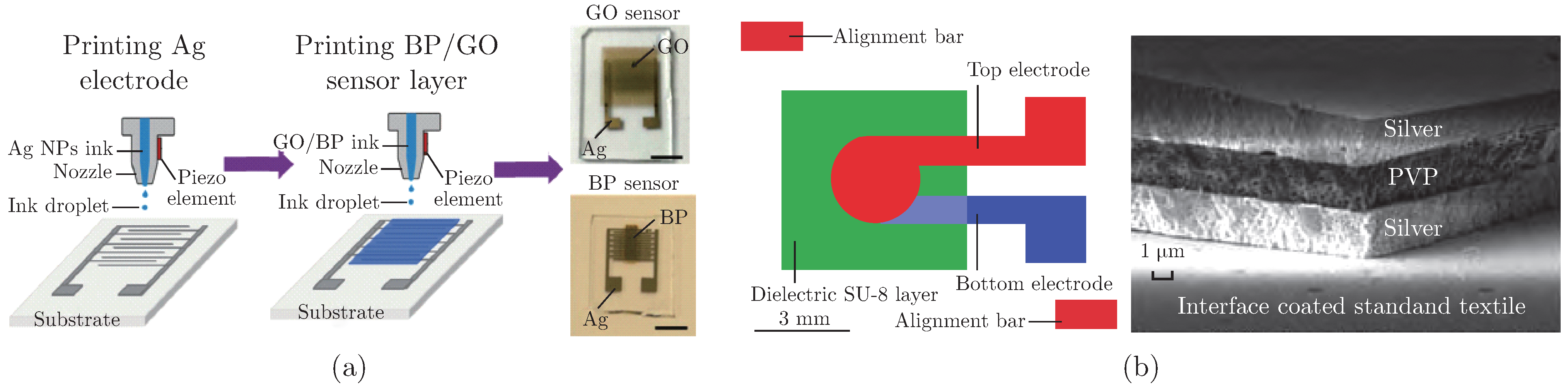
(a) Inkjet print humidity sensor based on graphene oxide and black phosphorus [64] ©Royal Society of Chemistry 2018 (b) Inkjet printed capacitor on the 65/35 polyester/cotton fabric [65] ©Copyright 2018 IEEE.
The strain, pressure and touch can be detected by resistance or capacitance change. For instance, a fully inkjet printed capacitive tactile sensor is fabricated by two silver layer and one dielectric layer [65] (see Figure 4(b)). The middle layer is using a solution consisting of PVP and a poly(melamine-co-formaldehyde) methylated solution in 1-hexanol. The UV-cured PVP layer thickness was 4.5 µm and the silver thickness was around 4-5 µm. However, nanometre-sized air bubbles have been found in the dielectric layer that influences the dielectric properties. Therefore, the dielectric ink should be further developed.
3.3. Inkjet Printed Transistors
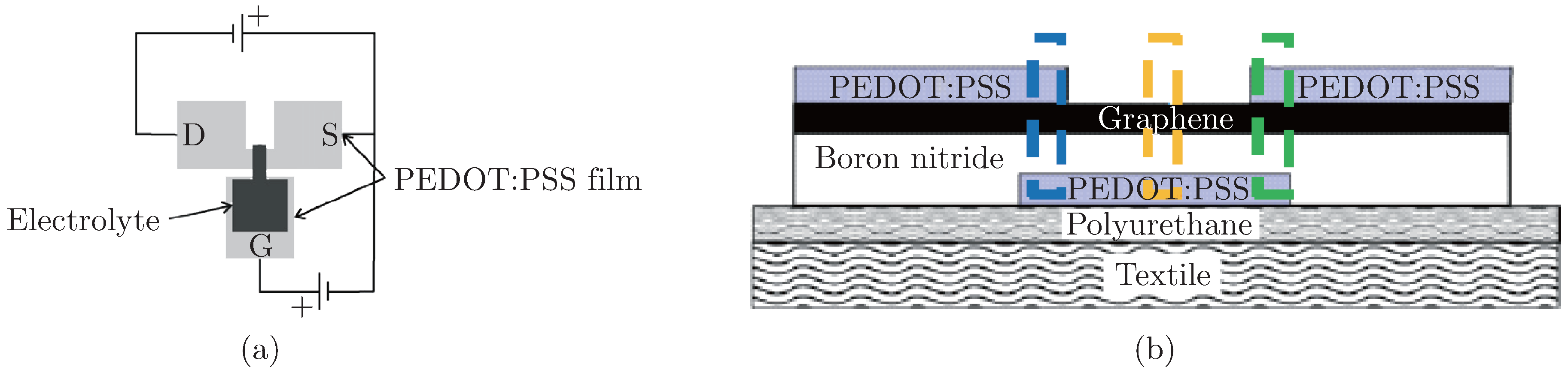
An electrochemical organic electronics are reported to inkjet print on standard inkjet photo paper and inkjet transparency film. Figure 5(a) illustrates the lateral design of the transistor. The PEDOT: PSS patterns act as electrodes and the water-based poly(sodium 4-styrenesulfonate) (PSS) acts as the electrolyte [62]. However, the device performances should be fine-tuned through developing better inkjet printable electrolytes. After that, the graphene and hexagonal-boron nitride (h-BN) inks are reported to fabricate all inkjet-printed flexible and washable field-effect transistors on textile [42]. Figure 5(b) explains the printing process of transistors. Polyurethane is coated on the polyester stain fabric to reduce the surface roughness. Then, a PEDOT:PSS film is firstly printed as the gate electrode, followed by a h-BN dielectric layer. Then a thin graphene channel is printed and finally deposited the PEDOT:PSS source and drain contacts. The field effect mobility reaches ∼91 cm2 V−1 s−1, at low voltage (<5 V).
Figure 5.
(a) Inkjet printed electrochemical organic electronics on photo paper and transparency film [62] ©2008 Elsevier B.V. (b) Inkjet-printed Field Effect Transistor on textile [42] ©2018 Springer Nature Limited.
4. Conclusion
This paper reviews the potentials and challenges in inkjet printing conductive inks on textile materials. The inkjet printing techniques have achieved high conductivity and low-cost electronic devices on flexible substrates like PET, PDMS and Kapton film. Therefore, it is believed to have great potential for textile substrates. However, the challenges exist in the complicated interaction between the liquid and porous medium. The ink easily penetrates through the thickness of fabric and then spreads along the yarns due to capillary force, so it is difficult to achieve the continuous printed line on textile substrates. The conventional approach is coating a hydrophobic layer on the yarn or fabric surface to overcome the surface roughness, but the compatibility between various layers is hard to achieve. Another approach to overcoming the porous structure is electroless plating, but the poor conductivity and low printed resolution are not suitable to produce electronic circuits. Also, the applications like electrodes, sensors and transistors are discussed here. Although most applications are fabricated on glass, silicone and many films, the textile substrate has potential with the development of inks.
Acknowledgments
We would like to thank Punjab Education Endowment Fund (PEEF), the EU Horizon 2020 and University of Manchester through projects with project codes 644268-ETEXWELD-H2020MSCA-RISE-2014, AA14512 (UMRI project “Graphene-Smart Textiles E-Healthcare Network”) and the British Cotton Growing Association Work People’s Collection Fund for funding the project “Protective Efficiency of Respiratory Protective Equipment (RPE) against Byssinosis for Cotton Workers” to provide support for this research.
References
- Tao, X. Handbook of smart textiles; 2015. [Google Scholar]
- Maleszka, T.; Kabacik, P. Bandwidth properties of embroidered loop antenna for wearable applications. Wirel. Technol. Conf. (EuWIT), 2010 Eur., No. September. 2010; pp. 89–92. [Google Scholar]
- Lim, Y. Y. Printing conductive traces to enable high frequency wearable electronics applications; 2015. [Google Scholar]
- Kamyshny, A. Metal-based Inkjet Inks for Printed Electronics. Open Appl. Phys. J. 2011. [Google Scholar] [CrossRef] [Scilit]
- Rida, A.; Yang, L.; Vyas, R.; Tentzeris, M. M. Conductive inkjet-printed antennas on flexible low-cost paper-based substrates for RFID and WSN applications. IEEE Antennas Propag. Mag. 2009, Vol. 51(No. 3), 13–23. [Google Scholar] [CrossRef] [Scilit]
- Hassan, A.; Ali, S.; Hassan, G.; Bae, J.; Lee, C. H. Inkjet-printed antenna on thin PET substrate for dual band Wi-Fi communications. Microsyst. Technol. 2017. [Google Scholar] [CrossRef] [Scilit]
- Wu, J.; Roberts, R. C. C.; Tien, N. C. C.; Li, D. Inkjet printed silver patterning on PDMS to fabricate microelectrodes for microfluidic sensing. Proceedings of IEEE Sensors, 2014; Vol. 2014-Decem, No. December. pp. 1100–1103. [Google Scholar]
- Virtanen, J.; et al. The effect of conductor thickness in passive inkjet printed RFID tags. 2010 IEEE International Symposium on Antennas and Propagation and CNC-USNC/URSI Radio Science Meeting-Leading the Wave, AP-S/URSI 2010, 2010. [Google Scholar]
- Patnaik, A.; Rengasamy, R. S.; Kothari, V. K.; Ghosh, A. Wetting and wicking in fibrous materials. Text. Prog. 2006, Vol. 38(No. 1), 1–111. [Google Scholar] [CrossRef] [Scilit]
- Whittow, W. G.; et al. Inkjet-printed microstrip patch antennas realized on textile for wearable applications. IEEE Antennas Wirel. Propag. Lett. 2014. [Google Scholar] [CrossRef] [Scilit]
- Nechyporchuk, O.; Yu, J.; Nierstrasz, V. A.; Bordes, R. Cellulose Nanofibril-Based Coatings of Woven Cotton Fabrics for Improved Inkjet Printing with a Potential in E-Textile Manufacturing, ACS Sustain. Chem. Eng. 2017, Vol. 5(No. 6), 4793–4801. [Google Scholar] [CrossRef] [Scilit]
- He, P. Inkjet Printing of Two Dimensional Materials A thesis Submitted to the University of Manchester. 2016. [Google Scholar]
- Cie, C. Ink Jet Textile Printing; 2015. [Google Scholar]
- Hawkyard, C. Substrate preparation for ink-jet printing. In Digital Printing of Textiles; 2006; pp. 201–217. [Google Scholar]
- Yi, Y.; Li, Y. Potentials and Challenges in Inkjet Printing Conductive Inks on Textile Materials. In Textile Bioengineering and Informatics Symposium; 2018, 2018; pp. 252–261. [Google Scholar]
- Cummins, G.; Desmulliez, M. P. Y. Inkjet printing of conductive materials: a review. Circuit World 2012, Vol. 38(No. 4), 193–213. [Google Scholar] [CrossRef] [Scilit]
- Kim, D.; Moon, J. Highly Conductive Ink Jet Printed Films of Nanosilver Particles for Printable Electronics. Electrochem. Solid-State Lett. 2005. [Google Scholar] [CrossRef] [Scilit]
- Bidoki, S. M.; Lewis, D. M.; Clark, M.; Vakorov, A.; Millner, P. A.; McGorman, D. Ink-jet fabrication of electronic components. J. Micromechanics Microengineering 2007, Vol. 17(No. 5), 967974. [Google Scholar] [CrossRef] [Scilit]
- Grancari’c, A. M.; et al. Conductive polymers for smart textile applications. J. Ind. Text. 2018. [Google Scholar] [CrossRef] [Scilit]
- Nguyen, B. H.; Nguyen, V. H. Promising applications of graphene and graphene-based nanostructures. Adv. Nat. Sci. Nanosci. Nanotechnol. 2016. [Google Scholar] [CrossRef] [Scilit]
- Ng, L. W. T.; et al. Printing of graphene and related 2D materials technology, formulation and applications; Springer, 2018. [Google Scholar]
- Fromm, J. E. Numerical Calculation of the Fluid Dynamics of Drop-on-Demand Jets. IBM J. Res. Dev. 1984, Vol. 28(No. 3), 322–333. [Google Scholar] [CrossRef] [Scilit]
- Reis, N.; Derby, B. Ink Jet Deposition of Ceramic Suspensions: Modeling and Experiments of Droplet Formation. MRS Proc. 2000, Vol. 625, 117. [Google Scholar] [CrossRef] [Scilit]
- Derby, B. Inkjet Printing of Functional and Structural Materials: Fluid Property Requirements, Feature Stability, and Resolution. Annu. Rev. Mater. Res. 2010, Vol. 40(No. 1), 395–414. [Google Scholar] [CrossRef] [Scilit]
- Torah, R.; Wei, Y.; Li, Y.; Yang, K.; Beeby, S.; Tudor, J. Printed textile-based electronic devices. In Handbook of Smart Textiles; 2015; pp. 653–687. [Google Scholar]
- Freire, E. M. Ink jet printing technology (CIJ/DOD). In Digital Printing of Textiles; 2006; pp. 29–52. [Google Scholar]
- Ujiie, H. Digital Printing of Textiles; 2006. [Google Scholar]
- Karaguzel, B.; Tafreshi, H. V.; Pourdeyhimi, B. Potentials and challenges in jetting microdroplets onto nonwoven fabrics. J. Text. Inst. 2008, Vol. 99(No. 6), 581–589. [Google Scholar] [CrossRef] [Scilit]
- Carr, W. W.; Park, H.; Ok, H.; Furbank, R.; Dong, H.; Morris, J. F. Drop formation and impaction. In Digital Printing of Textiles; 2006; pp. 53–68. [Google Scholar]
- Lim, Y. Y.; Goh, Y. M.; Liu, C.; Hutt, D. Surface modification of an ambient UV-cured dielectric to realise electrically conducting traces. Surf. Coat. Technol. 2015, Vol. 266, 93–104. [Google Scholar] [CrossRef] [Scilit][Green Version]
- Lee, J.; Oh, J. H.; Bae, H. S. Crack formation and substrate effects on electrical resistivity of inkjet-printed Ag lines. Mater. Lett. 2010, Vol. 64(No. 9), 1069–1072. [Google Scholar] [CrossRef] [Scilit]
- Wang, J. Z.; Zheng, Z. H.; Li, H. W.; Huck, W. T. S.; Sirringhaus, H. Dewetting of conducting polymer inkjet droplets on patterned surfaces. Nat. Mater. 2004, Vol. 3(No. 3), 171–176. [Google Scholar] [CrossRef] [Scilit]
- Ghahremani, M.; Latifi, M.; Babaei, M. Simulation of conductivity made by inkjet-printed silver tracks in E-textiles with different weave patterns. J. Ind. Text. 2016. [Google Scholar] [CrossRef] [Scilit]
- Karaguzel, Burcak. Printing Conductive Inks on Nonwovens: Challenges and Opportunities; 2007. [Google Scholar]
- Kissa, E. Wetting and Wicking. Text. Res. J. 1996, Vol. 66(No. 10), 660–668. [Google Scholar] [CrossRef] [Scilit]
- Ansari, N.; Kish, M. H. The wicking of water in yarn as measured by an electrical resistance technique. J. Text. Inst. 2000, Vol. 91(No. 3), 410–419. [Google Scholar] [CrossRef] [Scilit]
- Hollies, N. R. S.; Kaessinger, M. M.; Bogaty, H. Water Transport Mechanisms in Textile Materials Part Part I: The Role of Yarn Roughness in Capillary-Type Penetration. Text. Res. J. 1956, Vol. 27(No. 1), 829–835. [Google Scholar] [CrossRef] [Scilit]
- Kissa, E. Capillary sorption in fibrous assemblies. J. Colloid Interface Sci. 1981, Vol. 83(No. 1), 265–272. [Google Scholar] [CrossRef] [Scilit]
- Mhetre, S.; Carr, W.; Radhakrishnaiah, P. On the relationship between ink-jet printing quality of pigment ink and the spreading behavior of ink drops. J. Text. Inst. 2010, Vol. 101(No. 5), 423–430. [Google Scholar] [CrossRef] [Scilit]
- Chauraya, A.; et al. Inkjet printed dipole antennas on textiles for wearable communications. IET Microwaves Antennas Propag. 2013, Vol. 7(No. 9), 760–767. [Google Scholar] [CrossRef] [Scilit]
- Krykpayev, B.; Farooqui, M. F.; Bilal, R. M.; Vaseem, M.; Shamim, A. A wearable tracking device inkjet-printed on textile. Microelectron. J. 2017. [Google Scholar] [CrossRef] [Scilit]
- Carey, T.; et al. Fully inkjet-printed two-dimensional material field-effect heterojunctions for wearable and textile electronics. Nat. Commun. 2017, Vol. 8(No. 1). [Google Scholar] [CrossRef] [Scilit]
- Abadi, Z.; Mottaghitalab, V.; Bidoki, M.; Benvidi, A. Flexible biosensor using inkjet printing of silver nanoparticles. Sens. Rev. 2014, Vol. 34(No. 4), 360–366. [Google Scholar] [CrossRef] [Scilit]
- Bidoki, S. M.; Nouri, J.; Heidari, A. A. Inkjet deposited circuit components. J. Micromechanics Microengineering 2010, Vol. 20(No. 5). [Google Scholar] [CrossRef] [Scilit]
- Bidoki, S. M.; McGorman, D.; Lewis, D. M.; Clark, M.; Horler, G.; Miles, R. E. Inkjet printing of conductive patterns on textile fabrics. AATCC Rev. 2005, Vol. 5(No. 6), 11–14. [Google Scholar]
- Stempien, Z.; Rybicki, E.; Rybicki, T.; Lesnikowski, J. Inkjet-printing deposition of silver electroconductive layers on textile substrates at low sintering temperature by using an aqueous silver ions-containing ink for textronic applications. Sens. Actuators B Chem. 2015. [Google Scholar] [CrossRef] [Scilit]
- Kastner, J.; et al. Silver-based reactive ink for inkjet-printing of conductive lines on textiles. Microelectron. Eng. 2017, Vol. 176, 84–88. [Google Scholar] [CrossRef] [Scilit]
- Karim, N.; et al. All inkjet-printed graphene-based conductive patterns for wearable e-textile applications. J. Mater. Chem. C 2017, Vol. 5(No. 44), 11640–11648. [Google Scholar] [CrossRef] [Scilit]
- Sridhar, A.; Reiding, J.; Adelaar, H.; Achterhoek, F.; Van Dijk, D. J.; Akkerman, R. Inkjetprinting- and electroless-plating- based fabrication of RF circuit structures on high-frequency substrates. J. Micromechanics Microengineering 2009, Vol. 19(No. 8). [Google Scholar] [CrossRef] [Scilit]
- Zhang, C.; Fang, K. Surface modification of polyester fabrics for inkjet printing with atmosphericpressure air/Ar plasma. Surf. Coat. Technol. 2009, Vol. 203(No. 14), 2058–2063. [Google Scholar] [CrossRef] [Scilit]
- Shen, T.; Liu, Y.; Zhu, Y.; Yang, D.-Q.; Sacher, E. Improved adhesion of Ag NPs to the polyethylene terephthalate surface via atmospheric plasma treatment and surface functionalization. Appl. Surf. Sci. 2017, Vol. 411. [Google Scholar] [CrossRef] [Scilit]
- Meissner, M. V.; et al. Ink-jet printing technology enables self-aligned mould patterning for electroplating in a single step. J. Micromechanics Microengineering 2015, Vol. 25(No. 6). [Google Scholar] [CrossRef] [Scilit]
- Lok, B. K.; Ng, P. Y.; Hu, X.; Low, H. P. Effect of plasma treated ITO substrate on inkjet printing of conductive ink. In Proceedings of the Electronic Packaging Technology Conference, EPTC, 2006; pp. 154–160. [Google Scholar]
- Dearden, A. L.; Smith, P. J.; Shin, D. Y.; Reis, N.; Derby, B.; O’Brien, P. A low curing temperature silver ink for use in ink-jet printing and subsequent production of conductive tracks. Macromol. Rapid Commun. 2005. [Google Scholar] [CrossRef] [Scilit]
- Madorsky, S. L.; Hart, V. E.; Straus, S. Thermal degradation of cellulosic materials. J. Res. Natl. Bur. Stand. (1934) 1958, Vol. 60(No. 4), 343–349. [Google Scholar]
- Walker, S. B.; Lewis, J. A. Reactive silver inks for patterning high-conductivity features at mild temperatures. J. Am. Chem. Soc. 2012, Vol. 134(No. 3), 1419–1421. [Google Scholar] [CrossRef] [Scilit]
- Kim, K.; Il Ahn, S.; Choi, K. C. Simultaneous synthesis and patterning of graphene electrodes by reactive inkjet printing. Carbon N. Y. 2014, Vol. 66, 172–177. [Google Scholar] [CrossRef] [Scilit]
- Huang, X.; et al. Binder-free highly conductive graphene laminate for low cost printed radio frequency applications. Appl. Phys. Lett. 2015. [Google Scholar] [CrossRef] [Scilit]
- Beeby, S.; Li, Y.; Tudor, J.; Torah, R. Fully direct-write dispenser printed dipole antenna on woven polyester cotton fabric for wearable electronics applications. Electron. Lett. 2015, Vol. 51(No. 17), 1306–1308. [Google Scholar] [CrossRef] [Scilit]
- Whittow, W. G.; Li, Y.; Torah, R.; Yang, K.; Beeby, S.; Tudor, J. Printed frequency selective surfaces on textiles. Electron. Lett. 2014, Vol. 50(No. 13), 916–917. [Google Scholar] [CrossRef] [Scilit]
- Mohtaram, F.; Mottaghitalab, V.; Baghersalimi, G. Development and characterization of flexible antenna based on conductive metal pattern on polyester fabric. J. Text. Inst. 2017, Vol. 108(No. 11), 1888–1898. [Google Scholar] [CrossRef] [Scilit]
- Mannerbro, R.; Ranl¨of, M.; Robinson, N.; Forchheimer, R. Inkjet printed electrochemical organic electronics. Synth. Met. 2008, Vol. 158(No. 13), 556–560. [Google Scholar] [CrossRef] [Scilit]
- Cho, S. Y.; et al. Superior Chemical Sensing Performance of Black Phosphorus: Comparison with MoS2 and Graphene. Adv. Mater. 2016, Vol. 28(No. 32), 7020-+. [Google Scholar] [CrossRef] [Scilit]
- He, P.; et al. Fully printed high performance humidity sensors based on two-dimensional materials. Nanoscale 2018, Vol. 10(No. 12). [Google Scholar] [CrossRef] [Scilit]
- Li, Y.; Torah, R.; Beeby, S.; Tudor, J. An all-inkjet printed flexible capacitor on a textile using a new poly(4-vinylphenol) dielectric ink for wearable applications. Proceedings of IEEE Sensors, 2012. [Google Scholar]

© 2019 Textile Bioengineering and Informatics Society. This article is an open access article distributed under the terms and conditions of the Creative Commons Attribution (CC BY) license (https://creativecommons.org/licenses/by/4.0/).