Article

An Assessment of Thermoset Injection Molding for Thin-Walled Conformal Encapsulation of Board-Level Electronic Packages

1
Hahn-Schickard, 70569 Stuttgart, Germany
2
University of Stuttgart, Institute for Micro Integration (IFM), 70569 Stuttgart, Germany
*
Author to whom correspondence should be addressed.
J. Manuf. Mater. Process. 2019, 3(1), 18; https://doi.org/10.3390/jmmp3010018
Submission received: 21 December 2018 / Revised: 24 January 2019 / Accepted: 25 January 2019 / Published: 1 February 2019

Abstract

:
An ever-growing market demand for board (second) level packages (e.g., embedded systems, system-on-a-chip, etc.) poses newer challenges for its manufacturing industry in terms of competitive pricing, higher reliability, and overall dimensions. Such packages are encapsulated for various reasons including thermal management, protection from environmental conditions and dust particles, and enhancing the mechanical stability. In the due course of reducing overall sizes and material saving, an encapsulation as thin as possible imposes its own significance. Such a thin-walled conformal encapsulation serves as an added advantage by reducing the thermo-mechanical stresses occurring due to thermal-cyclic loading, compared to block-sized or thicker encapsulations. This paper assesses the encapsulation process of a board-level package by means of thermoset injection molding. Various aspects reviewed in this paper include the conception of a demonstrator, investigation of the flow simulation of the injection molding process, execution of molding trials with different encapsulation thicknesses, and characterization of the packages. The process shows a high dependence on the substrate properties, injection molding process parameters, device mounting tolerances, and device geometry tolerances. Nevertheless, the thermoset injection molding process is suitable for the encapsulation of board-level packages limiting itself only with respect to the thickness of the encapsulation material, which depends on other external aforementioned factors.

1. Introduction

The production of packages at different levels plays a major role in the microassembly technology [1]. The wide range of different requirements related to packaging solutions in the fields of automotive, medical, and automation industries is also increasing by the day [2]. The requirement of integrating more and more functions in an electronic assembly stimulates more challenges regarding miniaturization, robustness, reliability, and cost reduction in manufacturing [3]. Encapsulations are used to protect the electronic components from adverse environmental conditions and mechanical shock, and to undertake the functions of structural support and electrical insulation [4]. Additionally, encapsulations assume the thermal management of the assembly. The use of epoxy molding compounds (EMC) for the encapsulation of packages offers a large set of advantages such as low coefficients of thermal expansion (CTE), decent thermal conductivity, good chemical stability, higher Young’s modulus, etc. [5]. Due to their reduced shrinkage and low viscosity values compared to thermoplastic materials, even highly sensitive electronic assemblies can be packaged owing to the possibility of processing at lower injection pressures. Packaging is carried out at various stages to enable system integration at different levels of complexity, which usually begins at the chip or wafer level [1] and has no upper limit. Table 1 gives examples of packages of different levels (up to the fourth level). This article deals with the encapsulation of the second level (or board-level) packages.
Transfer molding is the most commonly used technology for the encapsulation of microsystems [1]. For constant development and newer ideas, the application of an easily automatable, flexible, and cost-effective production method is needed. Furthermore, an injection molding machine can be flexibly used for thermoplastic and thermosetting plastics with suitable necessary attachments. Thermoset injection molding offers these required characteristics. A major portion of injection molding service providers already owns machines that can be easily upgraded to deploy the thermoset injection molding process. A small and medium-sized enterprise (SME) can profit from this availability to easily order for non-standard packages and in lower order volumes. The biggest hurdle in the use of thermoset injection molding, however, lies in constraining the material within the processing window with a temperature high enough to achieve minimum viscosity but not as high as to facilitate rapid curing of the material as explained in Refs. [6,7]. The feasibility of using thermoset injection molding for encapsulating board-level packages was checked and presented in a previous article [8]. As a conclusion from Ref. [8], and according to other pretests conducted in-house regarding filling behavior and mechanical properties, thermoset injection molding can be implemented for thin-walled encapsulations of board-level packages.
A further challenge is posed by limiting the wall thickness of the encapsulation to a minimum. This enables material saving, reduces the end size of an assembly and should lower the thermo-mechanical loading, e.g., at the solder joints. Thermoset injection molding has shown to be a cost-effective alternative for encapsulation of electronic components and assemblies [7]. However, the process needs to be verified to investigate the minimum possible encapsulation thickness that conforms to the profile of the printed circuit board (PCB) and the mounted devices. A well-suited process simulation is also required to reduce the risk of defects during the molding trials. Numerical simulation methods for thermoset injection molding have been available since the 80s, e.g., Ref. [9]. While numerical simulation methods for transfer molding of encapsulations are also already presented in the literature since the 90s [10], not many references are available in the field of simulation of thermoset injection molding for the encapsulation of microelectronic devices. Similarly, hardly any literature is found that lays the foundation for the implementation of thermoset injection molding specifically for the manufacturing of thin-walled conformal encapsulation using an EMC supplied in granular form. An effort to bridge this gap in the literature is made with the help of this article.
In the forthcoming sections, a concept for a demonstrator is introduced (Section 2.1), the process simulation is explained (Section 2.2), the lessons learned through the molding trials are described (Section 3.1), and the outcome of the characterization is discussed (Section 3.2). The interpretation from and conclusions of the results are laid down in Section 4.

2. Materials and Methods

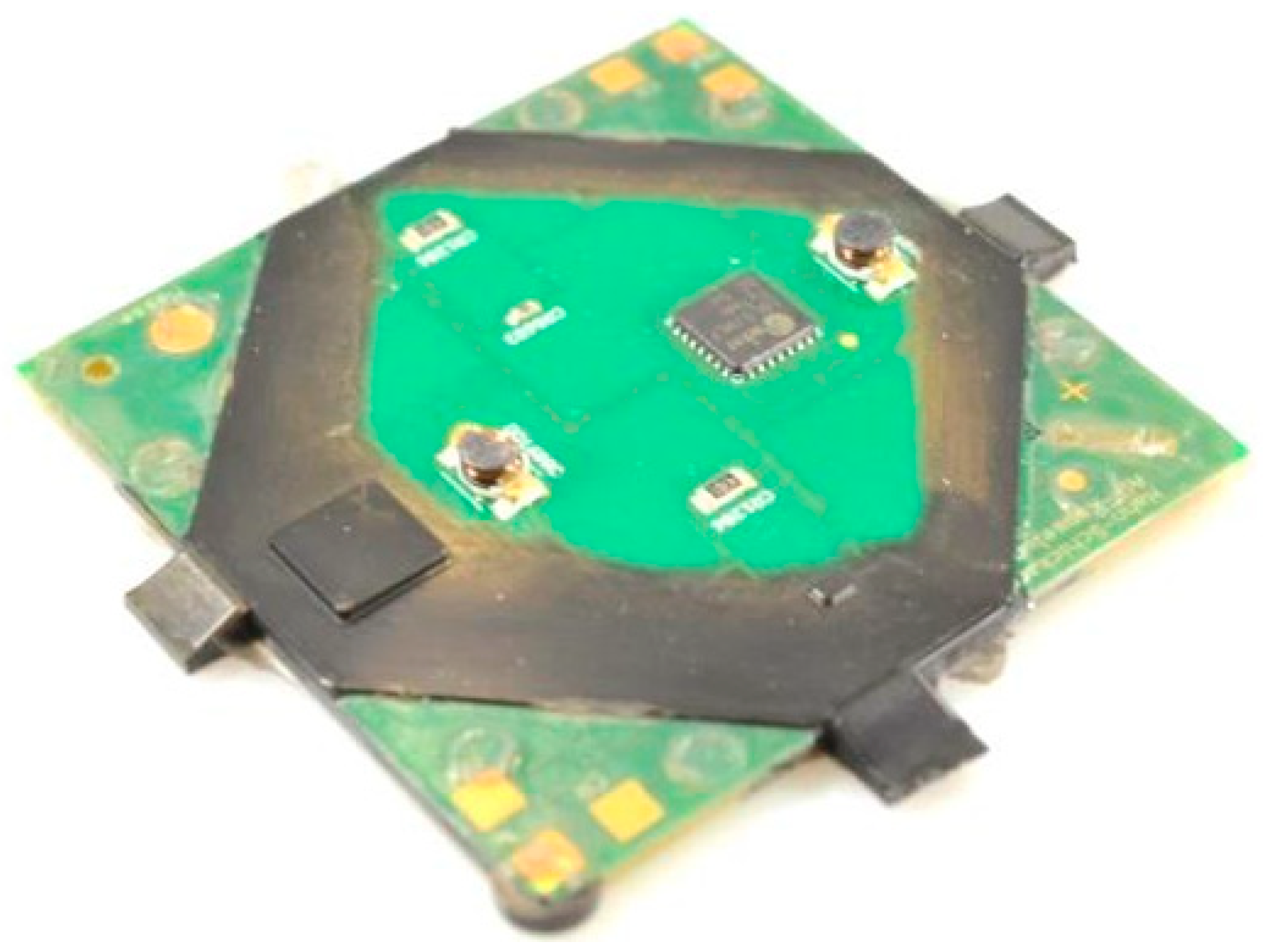
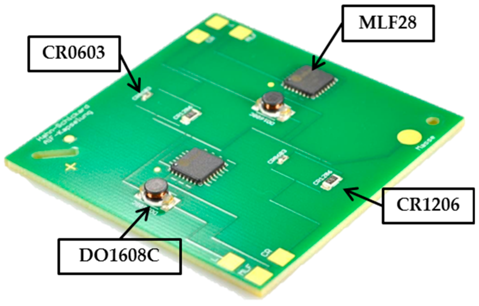
2.1. Conception of the Demonstrator

To investigate the above-mentioned important aspects regarding the implementation of thermoset injection molding for the encapsulation of board-level packages, an exemplary PCB (55 mm × 55 mm × 1.55 mm) with mounted devices was considered as shown in Figure 1. The demonstrator is based on a PCB with a relatively high glass transition temperature (Tg = 170 °C) with devices mounted on it. Various electronic devices of different sizes and geometries were taken into account. Two ceramic resistors of standard sizes CR1206 (4.7 kΩ) and CR0603 (1 kΩ) were chosen to be mounted in a parallel configuration to each other. These are positioned (two of each) in a linear repeating pattern to facilitate the examination of the effects of being placed either near or far from the gating position. One of the possible four gating positions is shown in Figure 2. In a similar fashion, a micro-leadframe (MLF28), representing broad devices, and an induction coil (DO1608C), representing tall devices, were mounted on the other normal axis. The layout enables electric tests of each mounted device individually. This layout can also be effectively put into use for later implementation of inline failure detection during environmental tests in accordance with Refs. [11,12,13,14]. Figure 2 shows a CAD model of the demonstrator with a thin-walled encapsulation following the contour of the mounted devices.
Molding trials with different reducing encapsulation thicknesses were planned, starting from 1 mm. The further stages corresponded to thicknesses of 0.5 mm and 0.25 mm. Respectively, three different molding tool inserts (Figure 3 shows one example) fitted within the standard molding tool available in-house at Hahn-Schickard were machined using the milling process. The design supported molding trials in four directions, which allowed a closer contemplation of the flow behavior in each case.
The material for the encapsulation of the board-level packages was chosen from common suppliers in the European market for the EMCs deemed fit for a granular feed to enable reproducibility owing to easy availability for SMEs in the region. The chosen EMC is available in the market with the name NU6110V [15] from the manufacturer Duresco GmbH (Witterswil, Switzerland). The key properties of this material are shown in Table 2.

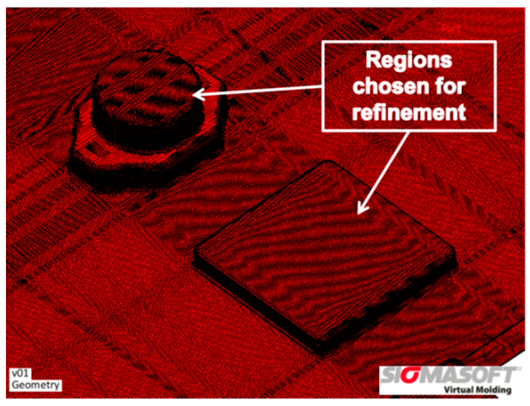
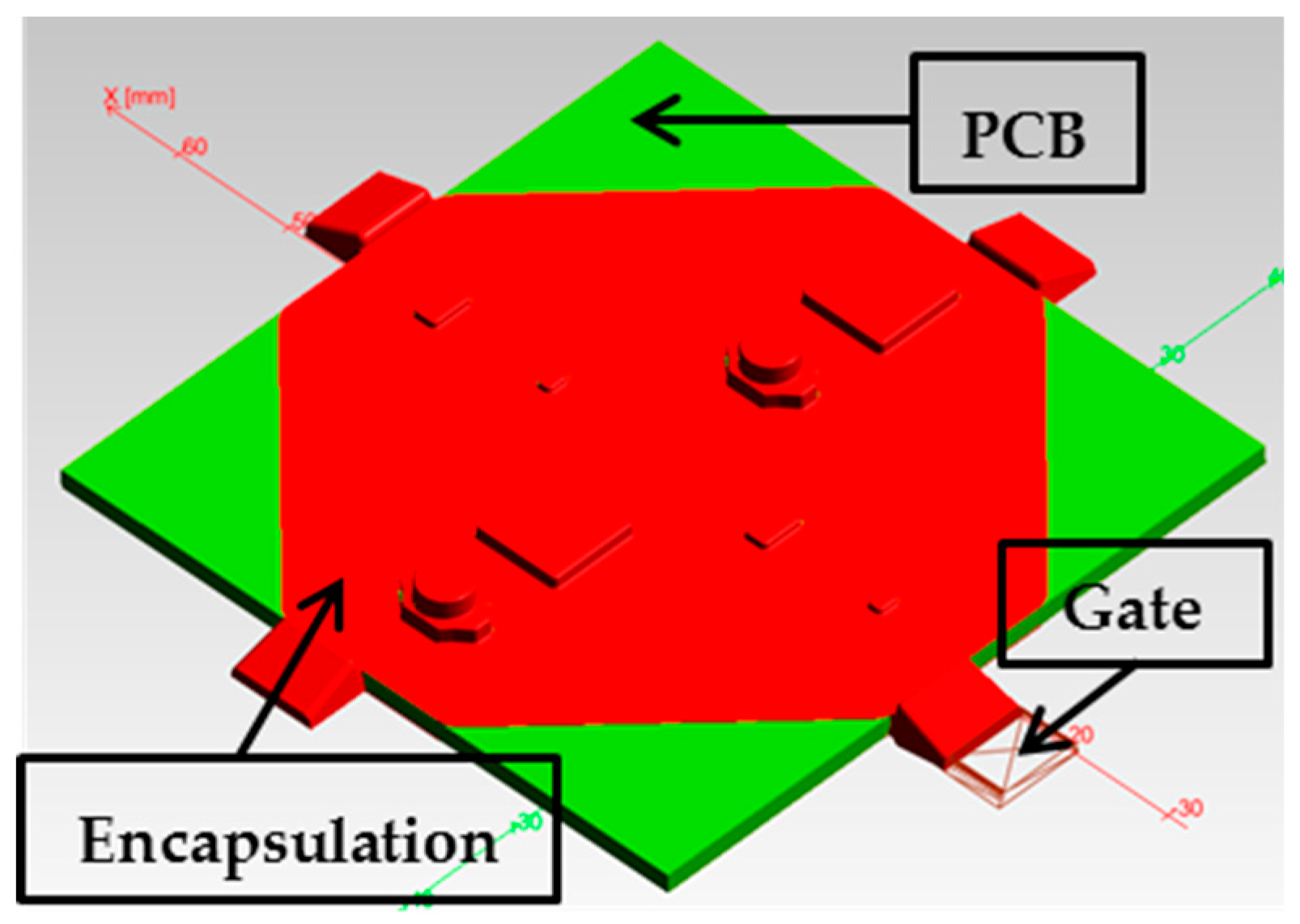
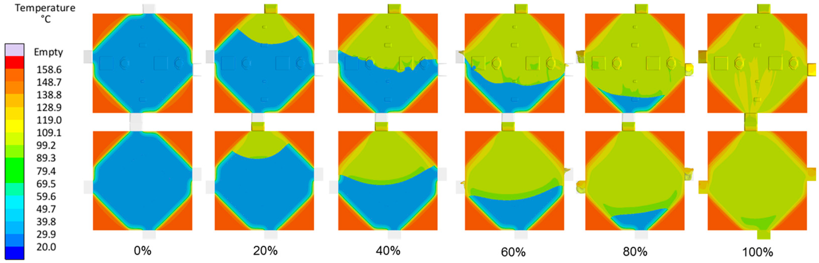
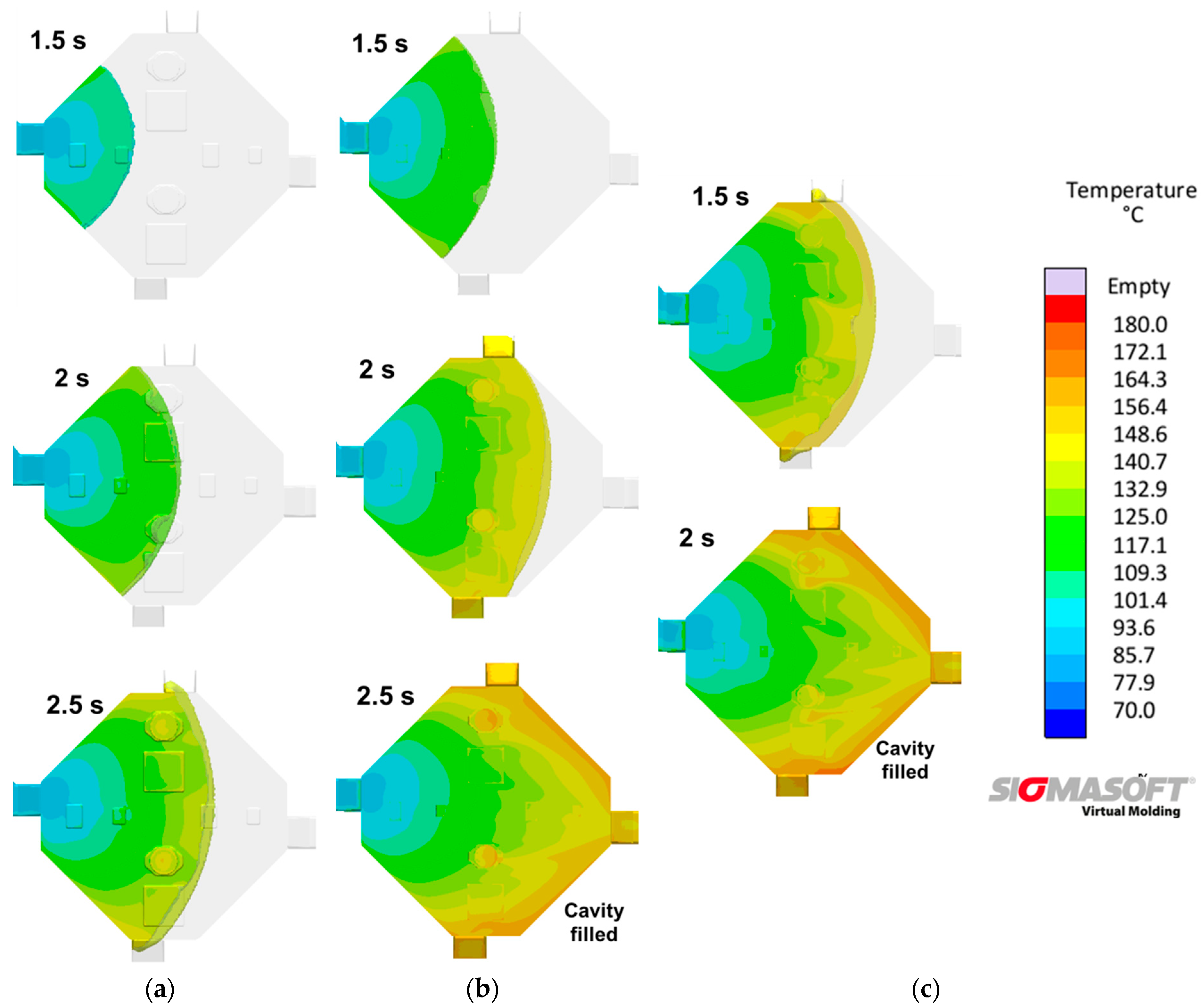
2.2. Process Simulation

Numerous iterations during molding trials can be effectively reduced by virtue of optimizing the encapsulation design in terms of sprue length, gate position, tempering channels, and injection parameters. The injection molding simulations were carried out using SIGMASOFT Virtual Molding (v5.2) provided by SIGMA Engineering GmbH (Aachen, Germany). Relevant results for the optimized gate positioning were also taken from an earlier in-house project [16] and verified with experiments during the same project and as presented in Ref. [17] involving the (film assisted) transfer molding process. These results recommended an offset positioning of the gate to the axis on which the devices were mounted in the flow direction to reduce the possibility of occurrence of weld-lines and voids in the flow shadow regions of the mounted devices.
The material model used for the simulation was based on an earlier version of the material [18], replenished with the help of data measured via external service providers, and confirmed by the material manufacturer and simulation software provider.
A computer aided design (CAD) model for the planned demonstrator was developed in Creo® Parametric 2.0 developed by PTC Inc. (Needham, MA, USA) and implemented in SIGMASOFT as illustrated in Figure 2. The PCB and the mounted devices (the board-level package) acted as insert components in the process simulation. A finer mesh (Figure 4) was generated in the areas near the mounted devices to enhance the accuracy of the simulation. An example of the fineness of the mesh is shown in Figure 5, which ensured a minimum of three element layers throughout the encapsulation thickness (except in the thin gaps under the devices).
Numerous simulations were carried out involving the four possible injection directions (each 90° apart). Figure 6 shows the fill behavior for one such direction. The filling behavior was seen to be acceptably uniform with a slightly slower filling above the induction coil (tall cylindrical part). Besides, the melt temperature while entering the gate region rose to 100 °C, which is a suitable filling temperature recommended by the material manufacturer. Attaining the right temperature is necessary to reach a compromise between the least possible viscosity of the melt during filling and maximum possible curing during the holding time (30–60 s) [19] after filling is complete as explained in Section 1. The mounted side of the PCB was seen to be filled faster than the unmounted side, which reduced the risk of formation of a large weld line on the former.
A comparison of the simulations for the filling patterns for the different levels of encapsulation thickness showed a similar behavior, though the filling speed was different owing to different filling volumes. The comparison can be seen in Figure 7.
The images in Figure 7 show the filled melt on a temperature scale at different time points measured after the injection start (1.5–2.5 s). The cavity with a 0.25 mm wall thickness was filled already at 2 s, 0.5 mm at 2.5 s, and 1 mm (filled cavity not shown) filled at 4 s after injection. Due to different wall thicknesses, the melts attained different temperature levels in each case (higher in the case of lesser wall thickness). Though the attained melt temperature was high (highest in the case of 0.25 mm thickness), the curing degree achieved at the end of filling was under 4% with an initial degree of 3% included in the feedstock. At the end of the packing and holding time, this variant attained a curing degree of 72%, which necessitated the requirement of an additional accelerated curing process after the injection molding process. The optimized simulation parameters are shown in Table 3. Every thickness variant showed a pressure requirement of a maximum of 250 bar, which is comfortably under the limits (≈2000 bar) of a common injection molding machine.
The simulation phase was, thus, concluded assuming that an acceptably good filling behavior would be achieved during the experimental molding trials. The resulting molding trials and the characterization that followed are presented in the forthcoming Section 3.

3. Results

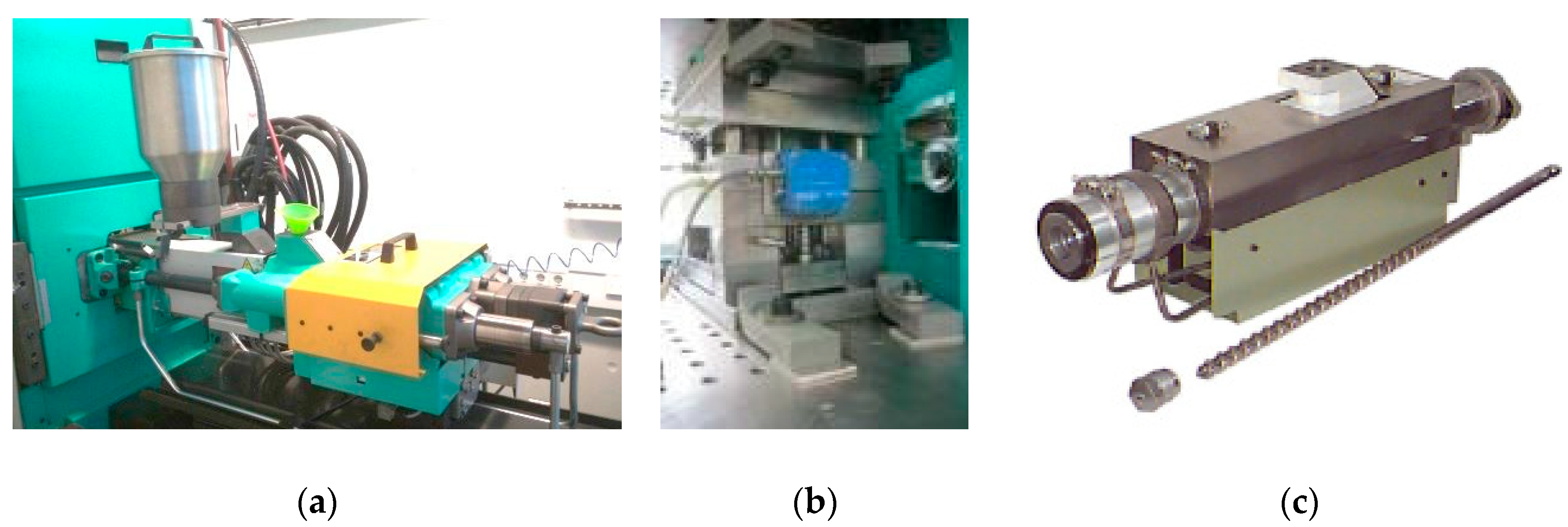
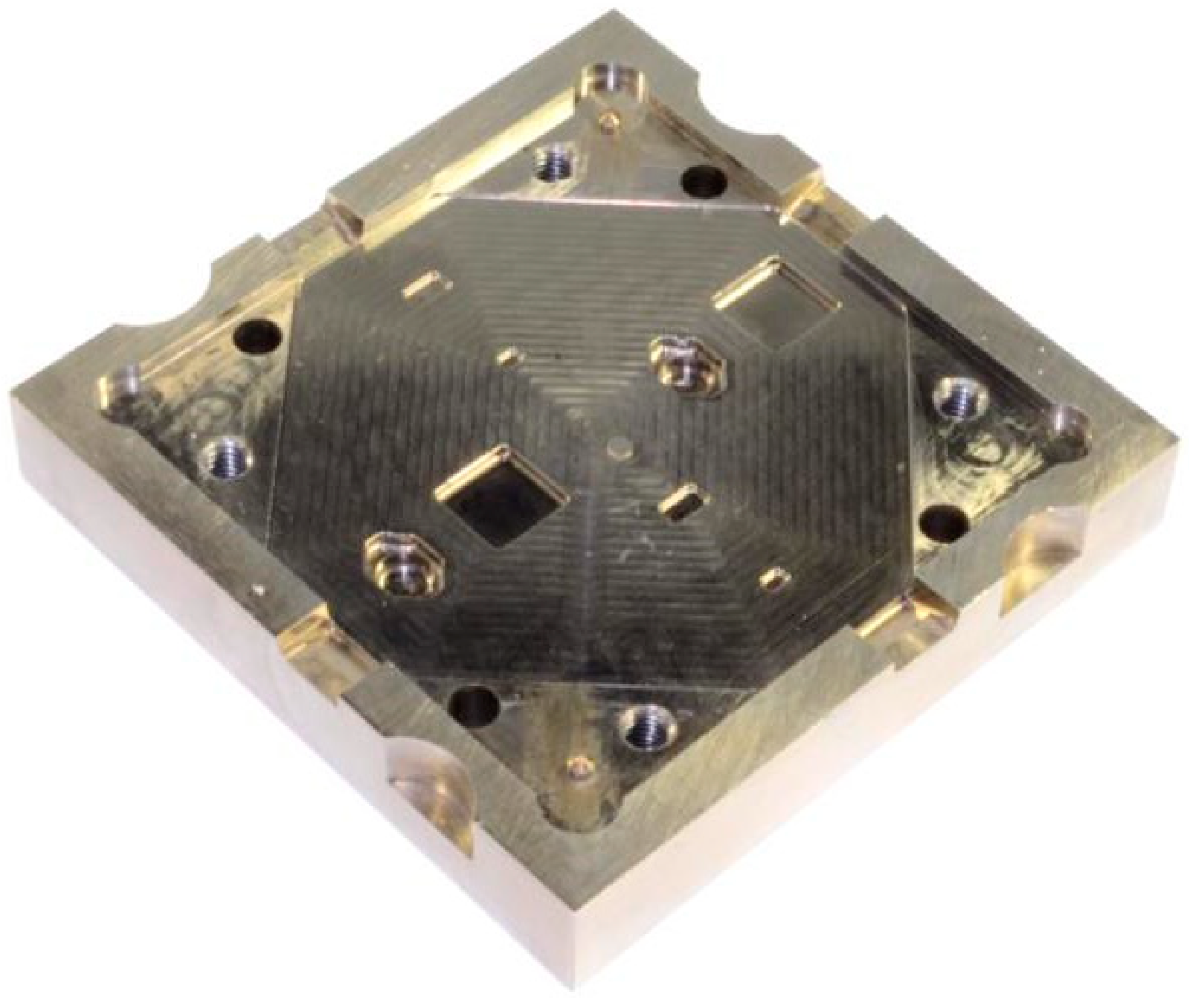
3.1. Experimental Molding Trials

All molding trials were carried out using a setup for thermoset injection molding at Hahn-Schickard as depicted in Figure 8 on a horizontal Arburg Allrounder 375 V (a), with a mounted standard molding tool (b), and an attachment (Ø 20 mm) suitable for processing of thermosetting plastics (c). The upper half of the molding tool was free to move only in the vertical direction. The lower half, which also held the board-level package to be encapsulated, was mounted on a turntable rotating around the vertical axis. The injection feeding system and the molding tool inserts were cleaned before every trial with the use of a melamine resin Meloplas MF 152 (white color) [20] provided by Raschig GmbH as recommended by the machine and EMC manufacturers. Having similar flow properties as the encapsulation material, Meloplas was also used for the filling study of the mold cavity. A minimum of 20 warming up cycles were taken up before every new molding trial. All packages were subjected to a drying step at 130 °C for 1 h before encapsulation. After encapsulation (injection molding procedure), the packages were placed into the oven for the accelerated completion of the cross-linking (curing) of the EMC. This involved holding the packages at the curing temperature (close to the mold temperature) of 150–180 °C for at least three hours as advised by the material manufacturer. As a comparison with market standards (and as a low-cost variant), PCBs with Tg = 125 °C were also investigated.
A test plan was made to correctly investigate all the possible combinations while involving the minimum consumption of PCBs. This test plan is shown in Figure 9. The tests were planned to start from the top-left corner, namely, the PCB with Tg = 125 °C and an encapsulation thickness of 1 mm. A successful molding trial was to be followed by a path led by a green arrow and an unsuccessful molding trial by a red arrow. In this way, it was ensured that the molding trials proceeded, as far as possible, using the PCBs with the lower Tg. When these PCBs were rendered useless in a particular molding trial, the same encapsulation thickness could be tested using the PCBs with the higher Tg. The subsequent molding trials would then be carried out only with the PCBs with the higher Tg (170 °C). A comparison of the values of thermal expansion coefficients of these two PCB variants is shown in Table 4.
A preliminary filling study (Figure 10) for the first molding trial (MT01) showed similar filling behavior to the simulation (Figure 6) on both sides of the PCB.
The molding trials (MT01) with an encapsulation thickness of 1 mm for the board-level packages based on the PCBs with Tg = 125 °C were successfully carried out. An encapsulated package from these molding trials is shown in Figure 11. No significant problems were noted during these trials. When sufficient packages were encapsulated with considerable repeatability, these molding trials for an encapsulation thickness of 1 mm were concluded. The injection molding setup was then retooled for the encapsulations with a 0.5 mm thickness.
The molding trials (MT02) based on the PCB with Tg = 125 °C and an encapsulation thickness of 0.5 mm were, however, not successful. Figure 12 shows an example of a large uncovered areas on the package. Various combinations of process parameters were tried out to remove this behavior. When all the combinations were rendered useless, a few samples were generated with holes drilled on the PCB at random positions to act as pressure equalizers between both sides of the PCB. These samples were then included in the molding trials. Nevertheless, these measures could not avoid the bending of the PCB as seen in Figure 13. As a further measure, a supporting pin was provided in the molding tool insert on the lower (mounted) side of the PCB to prevent it from bending. Thereafter, the molding trials were repeated, however, in vain. A stark bending of the PCB was still noticed in spite of the presence of the supporting pin and pressure equalizing in the form of drilled holes. The thermal expansion had, therefore, a very strong effect on the results of these molding trials. The molding trials were concluded as being unsuccessful and the path led by the red arrow as guided by Figure 9 was followed in the transverse direction.
Molding trials (MT02a) for the unchanged encapsulation thickness of 0.5 mm but for PCBs with Tg = 170 °C were conducted. The encapsulation process was successfully carried out even without the presence of the supporting pin and the pressure equalizing holes assuming the earlier set of process parameters. A few encapsulated samples, having equalizing holes, however, exhibited a lower injection pressure requirement.
The succeeding molding trials (MT03) according to the test plan in Figure 9 for thickness 0.25 mm and PCBs with Tg = 170 °C were conducted thereafter. They were partly successful. The filling behavior was acceptable, but minor uncovered areas on the mounted devices were discovered. The actual path followed on the test plan is marked and shown in Figure 14 by the blue dotted line. Further characterization of the encapsulations only from MT03 is discussed in detail in the next Section 3.2 due to its criticality and relevance of being the minimum thickness tested during the experiments.

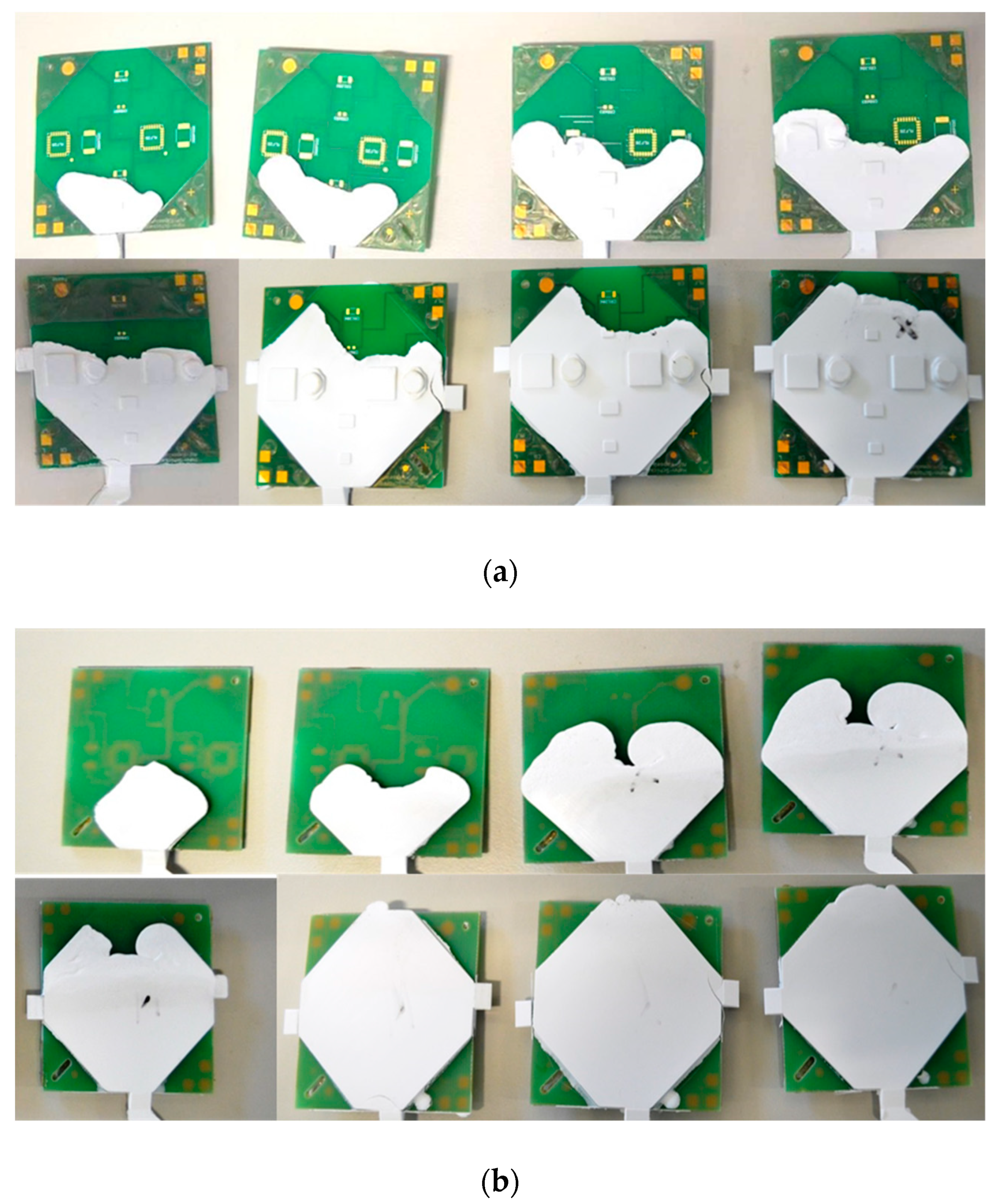
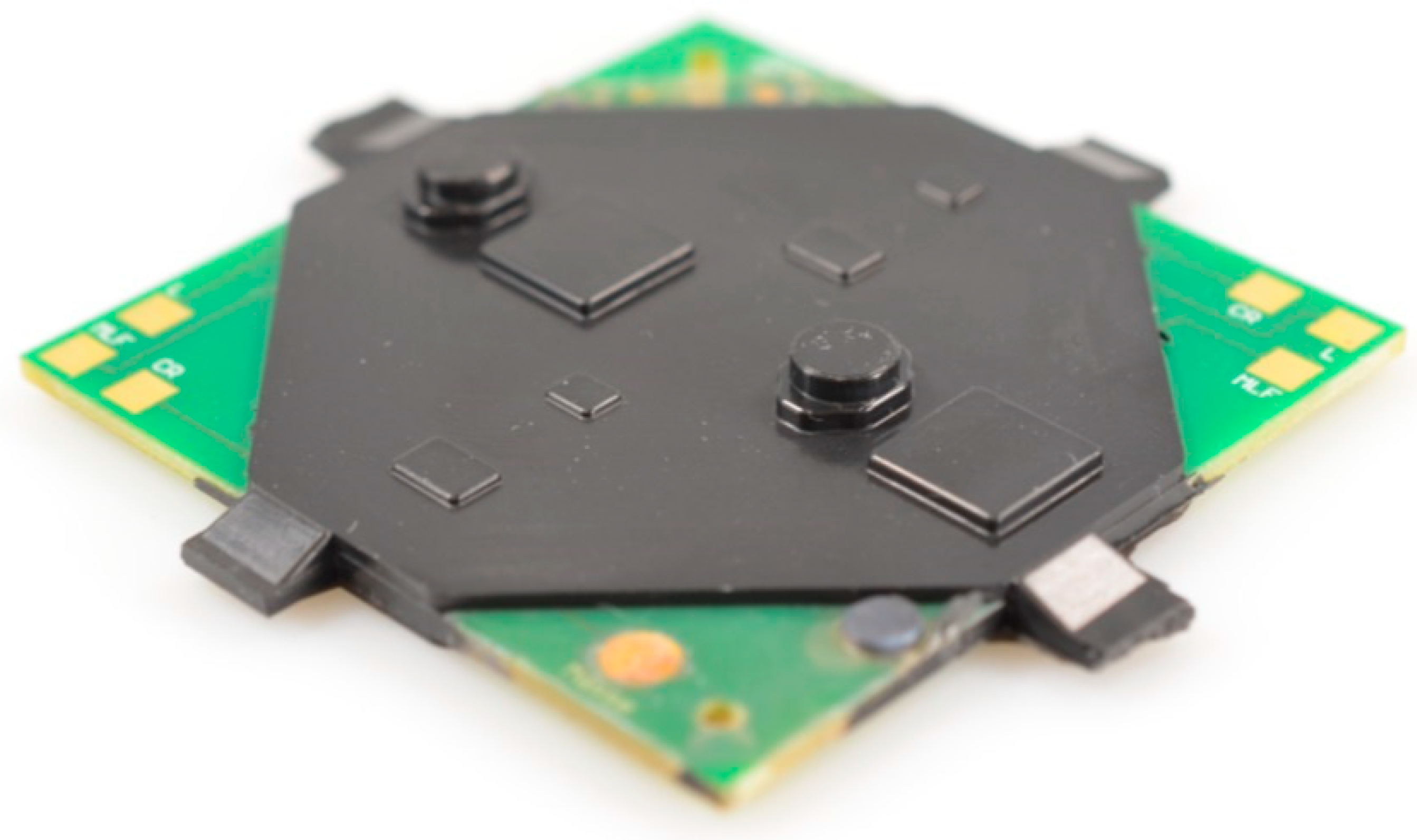
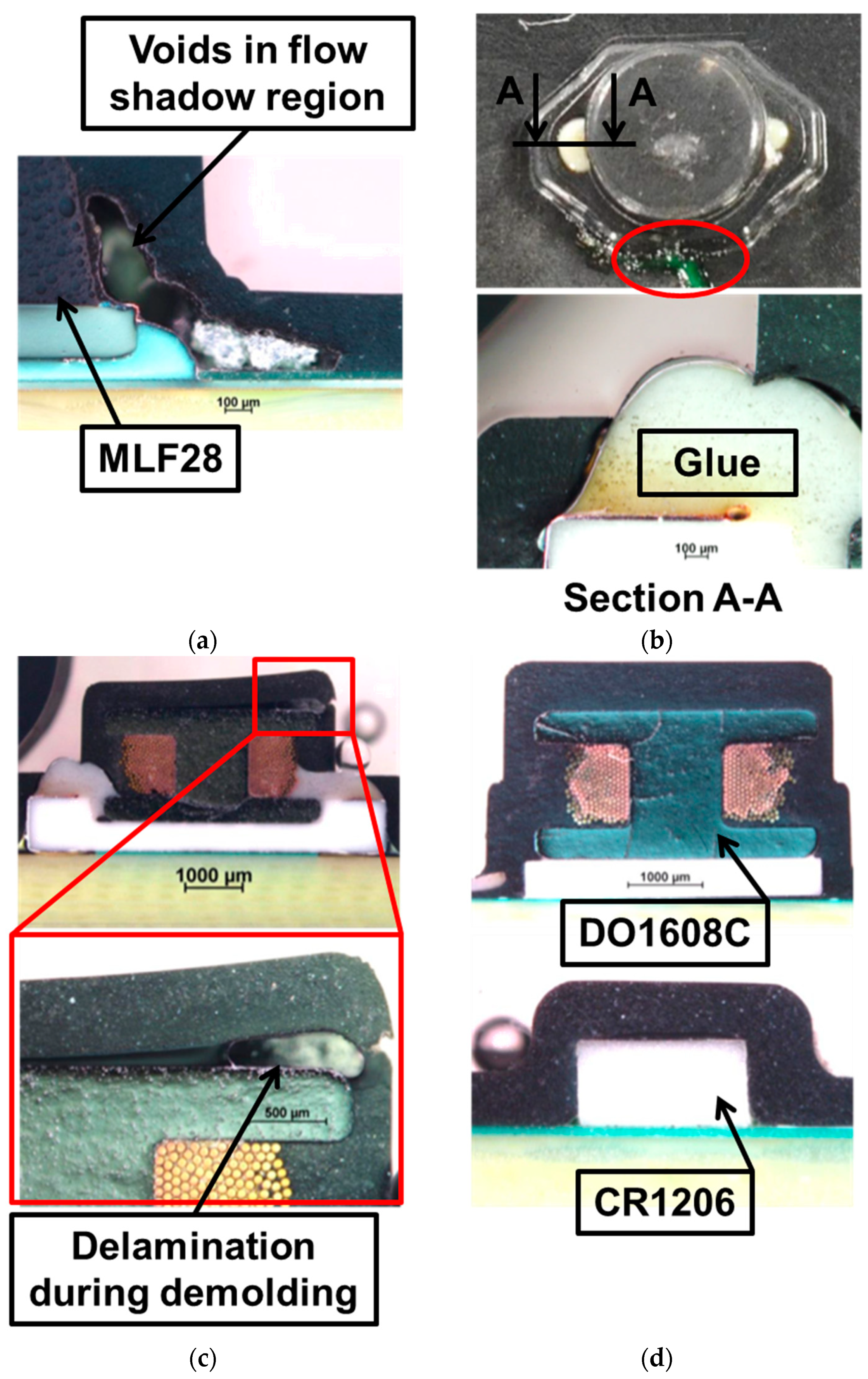
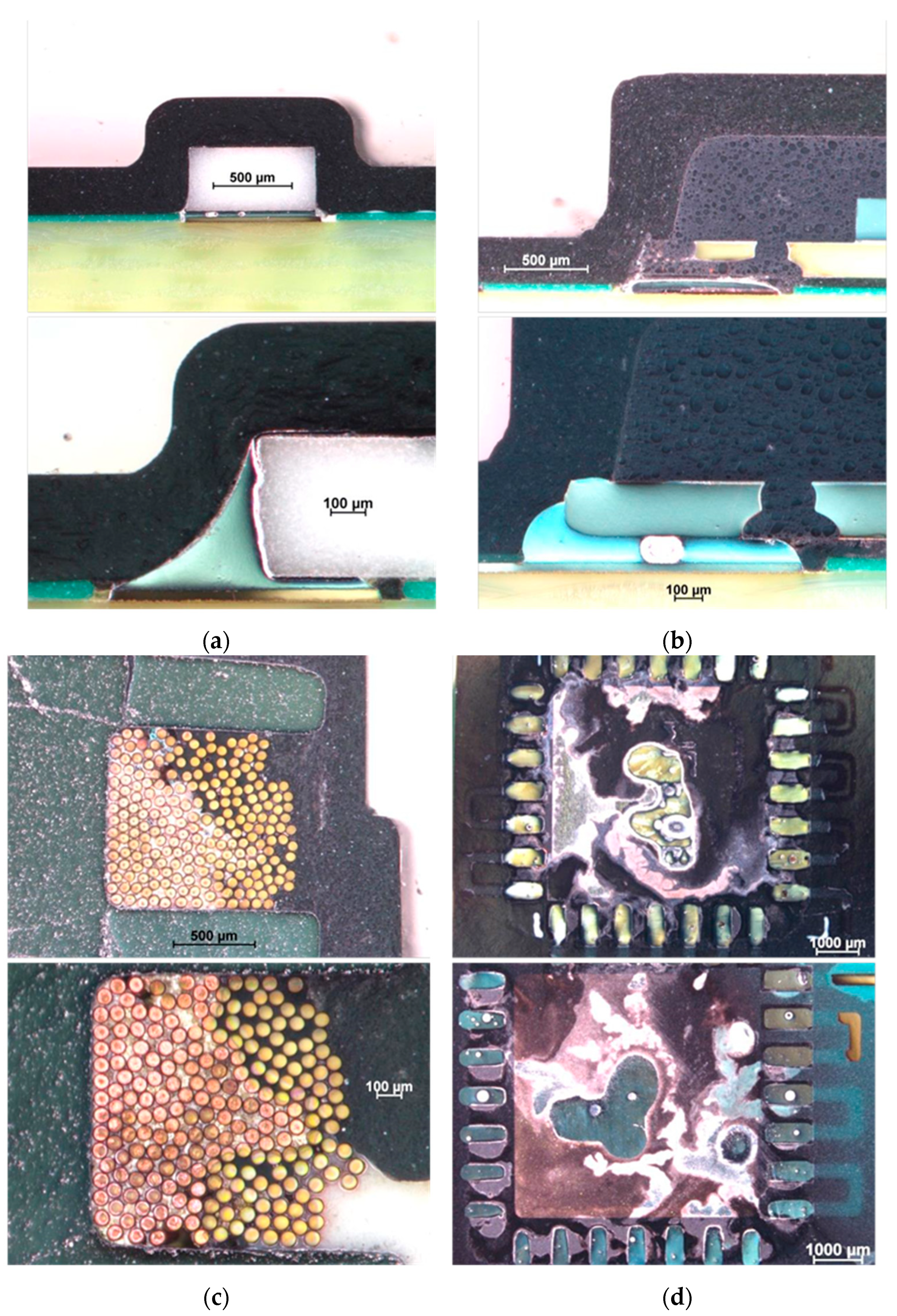
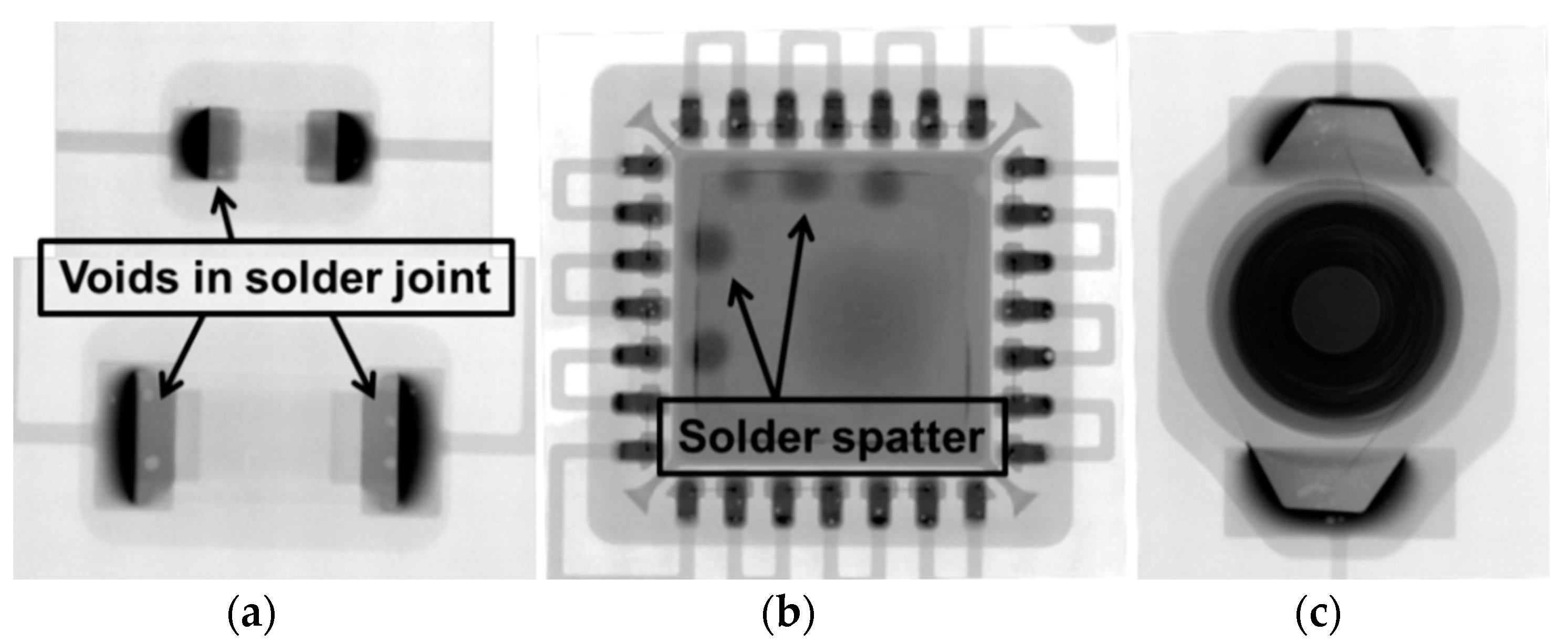
3.2. Characterization of the Encapsulation

The encapsulated samples were subjected to various stages of failure analysis. The PCBs were tested for electrical connectivity of all the mounted devices at the following stages:
  • after mounting of the electronic devices,
  • after the drying procedure/before injection molding,
  • after the injection molding process, and
  • after the accelerated curing at elevated temperatures.
After completion of the accelerated curing and stabilization of the packages at room temperature for a minimum of 24 h, randomly chosen packages were tested using X-ray scanning to look for any abnormalities present in the encapsulation. The images in Figure 15 shows examples of packages with well-filled encapsulations over the resistors (a), MLF (b), and the induction coil (c). A few void-like areas could be observed in each of the images, which were also noticed in the packages before encapsulation, corresponding to the typical voids in the solder joints. The smaller round-shaped darker regions in the image of the MLF (b) can be attributed to solder spatter, whereas the larger but less dark region may correspond with either an unfilled gap under the device or remnants of solder paste erroneously present in the no-contact region.
The encapsulation packages were then subjected to scanning acoustic microscopy (SAM) using an Echo STD by Sonix (Springfield, VA, USA) available in-house at Hahn-Schickard. Working on the principle of nondestructive ultrasonic flaw detection, this analysis helped to investigate the quality of the adhesion between the encapsulation and the PCB material. From the images in Figure 16, generated by using a 50 MHz transducer, it can be noted that the encapsulation held a good adhesion for a major part of the interface area with the PCB. Slight delamination occurred only in the areas near the edges of the encapsulation. This beginning of delamination occurred due to large aspect ratios between the length and the thickness of the encapsulation and a lack of mechanical anchorage, which was highly improved in enclosing packaging designs.
Later, randomly chosen samples underwent an advanced analysis process. Relevant cross-section planes were chosen and were probed using optical microscopy. As seen in Figure 17, the melt flowed through all regions for an encapsulation thickness of 0.25 mm, but developed a few air voids in the flow shadow areas of MLF28 (a). Apart from the similar problem of unfilled areas, a significant uncovered area can be noticed in the case of the induction coils (b) owing to the irregular shape and amount of the glue used in the manufacturing of the device. These devices have, compared to the accurate molding tool insert with 0.25 mm wall thickness, looser component geometry tolerances, which sometimes also led to delamination of the encapsulation from the top of the device during demolding (c). Likewise, the loose mounting tolerances also present a challenge to ensure a constant encapsulation thickness in all areas (d) especially in the lateral directions.
In areas where the tolerances of the devices and their mounting deviations were tighter than the encapsulation thickness, the problems mentioned do not occur. As seen in Figure 18, there were no air voids in the flow shadow areas of the resistor (a) and MLF (b), and no delamination of the encapsulation occurs during the demolding over the induction coil (c). Besides, the loose wires of the induction coil could also be successfully encapsulated (c). The thin gap under the MLF was also filled for a major part (d). This phenomenon can be possibly considered to provide an alternative to the need of using an underfill.
The characterization and the molding trials showed that the encapsulations with a layer thickness of 0.5 mm and 1 mm can be manufactured without hassles over board-level packages. A further study, involving the detailed characterization, reliability, and failure analysis is in progress. The results will be included in a future publication.

4. Discussions and Conclusions

The comparison of the filling simulation and the filling experimental study from the molding trials showed that the simulation with the available material model was sufficient to predict the filling behavior for a similar encapsulation application. However, the material model needed to advance to a higher level of accuracy in terms of better prediction of shrinkage and warpage (stress) calculations. This phenomenon is governed by the effects of temperature dependent pressure–volume curves for the melt and the cured material. The co-existence of the two phases makes it difficult for an accurate material model to be developed. The material manufacturers and the software providers are currently working together with research institutes that specialize in this field to improve this situation.
Owing to the outcome from the molding trials detailed in Section 3.1, it can be concluded that though thermoset injection molding demands use of PCBs with a higher Tg, encapsulations of 1 mm thickness of low-cost (standard) PCBs with lower Tg can also be manufactured.
The results of the characterization prove that board-level packages (PCB based) can be encapsulated with EMCs using thermoset injection molding with a minimal thickness of 0.25 mm. However, this encapsulation process is strongly dependent on device geometry and device mounting tolerances. Defects were observed during the characterization, which were not acceptable due to their high influence on the performance of the encapsulation. A medium-sized thickness of 0.5 mm or 1 mm is, therefore, recommended if the tolerances are either not constant or not tight enough within the expected limits. Besides, in case only the device mounting tolerances are relevant, the encapsulation wall thickness can be slightly increased only in the lateral directions.
Throughout the molding trials, a number of insights were gained. The following helpful measures for similar applications are recommended:
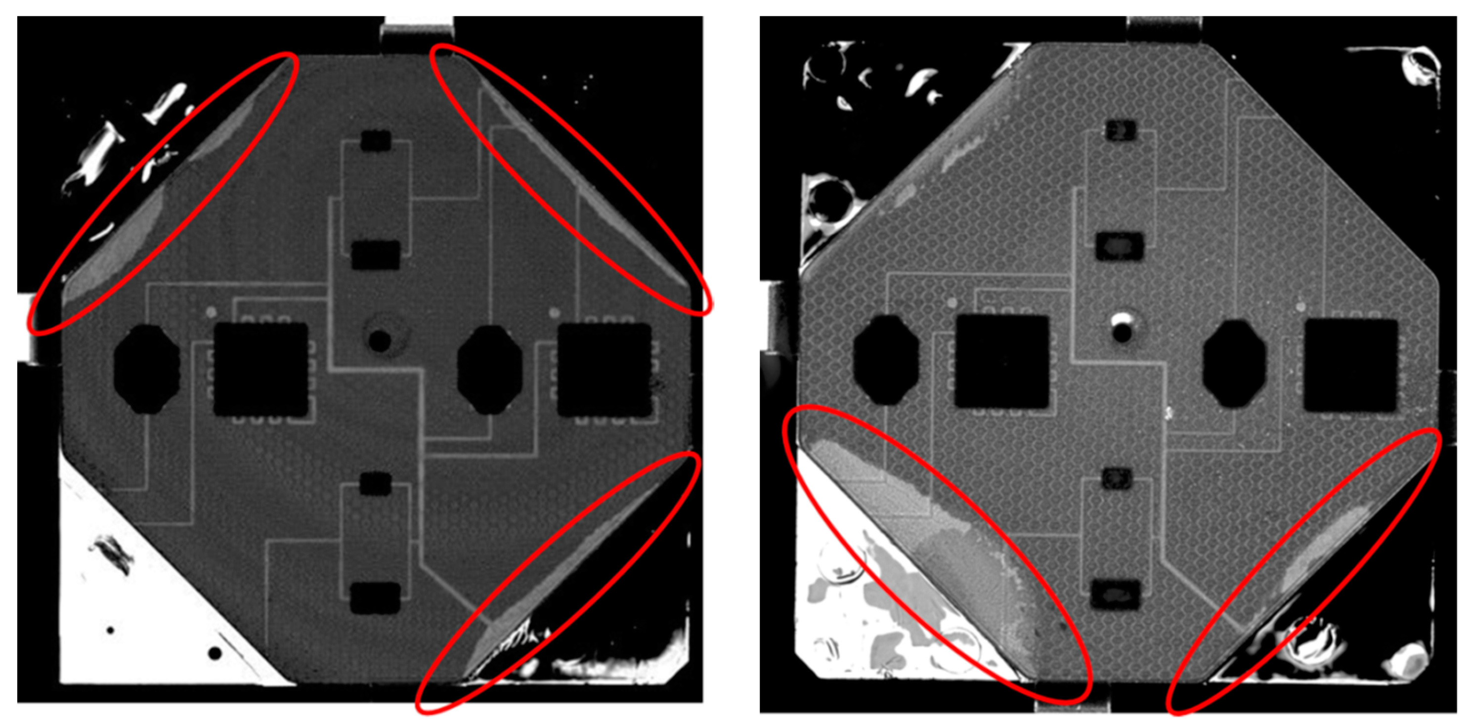
  • Areas around tall devices, e.g., induction coils or electrolytic capacitors, should be provided with, first, ample draft angles for easier demolding and to avoid delamination of the encapsulation, and second, with ejector pins that provide an additional function of venting the trapped air.
  • Ejector pins should also be placed in the sprue and melt overflow areas to avoid the material from staying behind in the cavity due to strong adhesion with metallic surfaces through curing and thereby blocking the way for further cycles and disrupting the repetitive process.
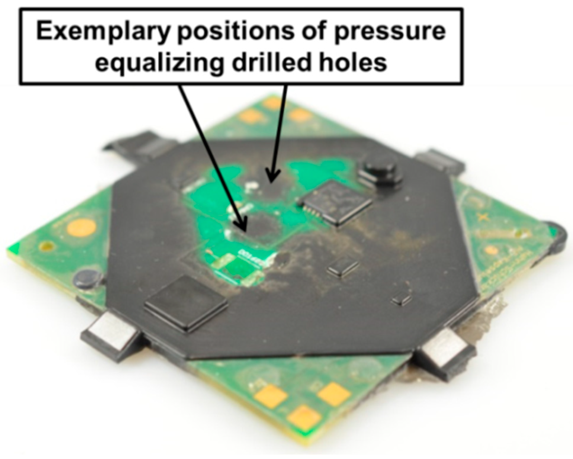
  • Pressure equalizing holes on the PCB are highly recommended. They serve an additional purpose of increasing the mechanical stability of the encapsulation.
With careful implementation, thermoset injection molding can be effectively deployed for the encapsulation of board-level packages with EMCs easily available in granular forms. SMEs can profit from this implementation by being able to procure non-standard encapsulated packages in medium (or even small) order sizes. A well-known and important hindrance in the development of microtechnology with respect to functional integration can, thus, be eliminated. Further work ongoing at Hahn-Schickard on this topic involves reliability analysis of such encapsulated packages/devices by applying already-existing lifetime models of solder joints based on the Coffin-Manson relation [11].

Author Contributions

Conceptualization, R.K. and T.G. (Thomas Guenther); methodology, R.K.; simulation, R.K.; experiments, P.W. and R.K.; characterization, R.K., M.H., and M.S.; writing—original draft preparation, R.K.; writing—review and editing, M.S., T.G. (Thomas Guenther), T.G. (Tobias Groezinger), and A.Z.; supervision, T.G. (Thomas Guenther) and T.G. (Tobias Groezinger); project administration, R.K.; funding acquisition, T.G. (Thomas Guenther) and A.Z.

Funding

This work was done in the scope of the research project AiF-Kapselung financed by the German Federation of Industrial Research Associations (AiF) as a part of the Industrial Collective Research (IGF) program by the German Federal Ministry for Economic Affairs and Energy (BMWi) (IGF Vorhaben Nr.: 18253 N). Authors would like to thank the different project partners and funding institutes.

Acknowledgments

The authors would like to thank the members of the project advisory group comprising of experts from the relevant industry domains for their valuable support and advice through the duration of project application and execution. Last but not the least; the authors are very thankful to the technical team at Hahn-Schickard and IFM for their quick and efficient processing of the internal assignments for this project.

Conflicts of Interest

The authors declare no conflict of interest.

References

  1. Ardebili, H.; Pecht, M. Encapsulation Technologies for Electronic Applications; William Andrew: Norwich, NY, USA, 2009; ISBN 978-0-8155-1970-6. [Google Scholar]
  2. Wilde, J. B4.1—Trends in Assembly and Packaging of Sensors. Proc. Sens. 2009, I, 205–210. [Google Scholar]
  3. Sensor-Trends 2014. Available online: https://www.ama-sensorik.de/fileadmin/Pubikationen/AMA_Trendbericht_Langfassung%5b1%5d.pdf (accessed on 30 January 2019).
  4. Manzione, L.T. Plastic Packaging of Microelectronic Devices; Van Nostrand Reinhold: New York, NY, USA, 1990. [Google Scholar]
  5. Kinjo, N.; Ogata, M.; Nishi, K.; Kaneda, A.; Dušek, K. Epoxy Molding Compounds as Encapsulation Materials for Microelectronic Devices. In Speciality Polymers/Polymer Physics; Advances in Polymer Science; Springer: Berlin/Heidelberg, Germany, 1989; pp. 1–48. ISBN 978-3-662-15081-8. [Google Scholar]
  6. Bonten, C. Kunststofftechnik: Einführung und Grundlagen; Carl Hanser Verlag GmbH Co KG: Munich, Germany, 2016. [Google Scholar]
  7. Beichter, S.; Weser, S.; Müller, H.; Petillon, S.; Haug, B.; Günther, T.; Eberhardt, W.; Zimmermann, A. Functionalized sensor packaging based on thermoset injection molding and selective metallization technology. In Proceedings of the 2015 European Microelectronics Packaging Conference (EMPC), Friedrichshafen, Germany, 14–16 September 2015. [Google Scholar]
  8. Kulkarni, R.; Hera, D.; Soltani, M.; Günther, T.; Grözinger, T.; Zimmermann, A. Feasibility of Manufacturing Packaged Electronic Systems by Thermoset Injection Molding. In Proceedings of the 11th Smart Systems Integration Conference 2017, Cork, Ireland, 8–9 March 2017. [Google Scholar]
  9. Kamal, M.R.; Ryan, M.E. The behavior of thermosetting compounds in injection molding cavities. Polym. Eng. Sci. 1980, 20, 859–867. [Google Scholar] [CrossRef]
  10. Turng, L.S.; Wang, V.W. On the Simulation of Microelectronic Encapsulation with Epoxy Molding Compound. J. Reinf. Plast. Compos. 1993, 12, 506–519. [Google Scholar] [CrossRef]
  11. Grözinger, T. Untersuchungen zu Zuverlässigkeit und Lebensdauermodellen für gelötete SMD auf spritzgegossenen Schaltungsträgern; Universität Stuttgart: Stuttgart, Germany, 2015. [Google Scholar]
  12. Wild, P.; Grözinger, T.; Lorenz, D.; Zimmermann, A. Void Formation and Their Effect on Reliability of Lead-Free Solder Joints on MID and PCB Substrates. IEEE Trans. Reliab. 2017, 66, 1229–1237. [Google Scholar] [CrossRef]
  13. Soltani, M.; Freyburger, M.; Kulkarni, R.; Mohr, R.; Groezinger, T.; Zimmermann, A. Development and Validation of a Novel Setup for LEDs Lifetime Estimation on Molded Interconnect Devices. Instruments 2018, 2, 28. [Google Scholar] [CrossRef]
  14. Soltani, M.; Freyburger, M.; Kulkarni, R.; Mohr, R.; Groezinger, T.; Zimmermann, A. Reliability Study and Thermal Performance of LEDs on Molded Interconnect Devices (MID) and PCB. IEEE Access 2018, 6, 51669–51679. [Google Scholar] [CrossRef]
  15. Technical Datasheet NU 6110V. Available online: https://yellowcards.ulprospector.com/certificate/e171477/duresco-nu-6110-v-nu-6110-t (accessed on 30 January 2019).
  16. Flexibles Packaging von Mikrosystemtechnischen Bauelementen Basierend auf Leiterplattenträgern mittels Film-Assisted-Molding. Available online: https://docplayer.org/9434933-Flexibles-packaging-von-mikrosystemtechnischen-bauelementen-basierend-auf-leiterplattentraegern-mittels-film-assisted-molding.html (accessed on 30 January 2019).
  17. Hera, D.; Berndt, A.; Günther, T.; Schmiel, S.; Harendt, C.; Zimmermann, A. Flexible Packaging by Film-Assisted Molding for Microintegration of Inertia Sensors. Sensors 2017, 17, 1511. [Google Scholar] [CrossRef] [PubMed]
  18. Technical Datasheet NU 5680. Available online: https://yellowcards.ulprospector.com/certificate/e195551/duresco-nu-5680-v (accessed on 30 January 2019).
  19. Deringer, T.; Gröschel, C.; Drummer, D. Influence of mold temperature and process time on the degree of cure of epoxy-based materials for thermoset injection molding and prepreg compression molding. J. Polym. Eng. 2018, 38, 73–81. [Google Scholar] [CrossRef]
  20. Technical Datasheet MELOPAS® MF 152. Available online: https://plastics.ulprospector.com/datasheet/e129510/melopas-mf-152 (accessed on 30 January 2019).
Figure 1. PCB with mounted devices (CR1206, CR0603, MLF28, DO1608C).
Jmmp 03 00018 g001
Figure 2. CAD model of the demonstrator for investigating the implementation of thermoset injection molding for thin-walled encapsulations of board-level packages.
Jmmp 03 00018 g002
Figure 3. Molding tool insert for a 0.25 mm thick encapsulation.
Jmmp 03 00018 g003
Figure 4. Fine mesh in the areas especially around the devices.
Jmmp 03 00018 g004
Figure 5. Exemplary fine mesh around the MLF with at least three elements over the wall thickness.
Jmmp 03 00018 g005
Figure 6. Simulated filling behavior (temperature scale) at different filling stages on the mounted (first row) and unmounted (second row) sides for an encapsulation thickness of 1 mm.
Jmmp 03 00018 g006
Figure 7. Comparative fill behavior from the simulation for (a) 1 mm, (b) 0.5 mm, and (c) 0.25 mm encapsulation thickness.
Jmmp 03 00018 g007
Figure 8. Setup for thermoset injection molding: (a) Arburg 375 V injection molding machine, (b) closed standard molding tool, and (c) attachment for processing of thermosetting plastics.
Jmmp 03 00018 g008
Figure 9. Test plan for the molding trials starting from top-left. A successful molding trial was to be followed by the green arrow and an unsuccessful molding trial was to be followed by the red arrow.
Jmmp 03 00018 g009
Figure 10. Filling behavior during MT01 on (a) mounting/front side but on an unmounted PCB, and (b) back side of the PCB.
Jmmp 03 00018 g010
Figure 11. Encapsulated (1 mm thick) board-level package.
Jmmp 03 00018 g011
Figure 12. Significant uncovered areas of the package during mold trials MT02 due to the bent PCB.
Jmmp 03 00018 g012
Figure 13. Pressure equalizing holes were also not useful in avoiding the PCB from bending during mold trials MT02.
Jmmp 03 00018 g013
Figure 14. Original test plan superimposed by the actual path followed (blue dotted line).
Jmmp 03 00018 g014
Figure 15. X-ray images of encapsulated devices (MT03): (a) resistors: voids in solder joint visible with no defect in the encapsulation; (b) MLF28: voids in solder joint, solder spatter and remnants of solder paste visible, and void in encapsulation in the gap under the device is possible; and (c) induction coil: voids in solder joint visible with no defect in encapsulation.
Jmmp 03 00018 g015
Figure 16. Images from the scanning acoustic microscopy at the interface of the PCB and the encapsulation. Except for a few delaminated areas (marked in red) at the edges, the encapsulation showed good adhesion with the PCB material.
Jmmp 03 00018 g016
Figure 17. Results from microscopic analysis I. (a) Voids were noticed in the flow shadow region of the MLF. (b) An uncovered area (marked red) was noticed between two devices and the irregular shape of the glue around the induction coil caused irregularities. (c) Delamination of the encapsulation from the holder of the induction coil was noticed due to a lower thickness available in the lateral direction. (d) An offset is seen in the positioning of the induction coil and the resistor that enforced the presence of non-uniform encapsulation thicknesses on both sides of the device.
Jmmp 03 00018 g017
Figure 18. Results from microscopic analysis II. (a) Resistors and (b) MLF had a well-filled encapsulation when no irregularities in the device geometry or mounting were present. (c) The loose wires of the induction coil also had a well-packed encapsulation. (d) The thin gap under the MLF was also filled, though only partly.
Jmmp 03 00018 g018
Table 1. Definition of different levels of packages according to Ref. [1]. (IC: integrated circuit, RAM: random-access memory).
LevelStage
0IC chip
1Encapsulated microelectronic package
2Printed circuit board with various mounted devices
3Multiple PCBs (e.g., RAM) integrated on a mother board
4Housed electronics system (e.g., laptop computer)
Table 2. Key properties of material NU6110V according to Ref. [15].
Material PropertyValue
Density2.0 g/cm3
Glass transition temperature160 °C
Thermal conductivity0.85 W/mK
Coefficient of thermal expansion (20–105 °C)18 ppm/K
Young’s modulus (flexural test)18 GPa
Table 3. Inputs used for the simulation.
MaterialNU 6110 V
Melt injection temperature70 °C
Mold tempering180 °C
Flow control (flux)2 cm3/s
Table 4. Comparison of the CTE values of the two PCB variants (ppm/K).
DirectionTg = 125 °CTg = 170 °C
X12.813.5
Y13.215.6
Z (below Tg)4355
Z (above Tg)242234

