


Abstract
Gas-insulated busducts (GIBs) require spacer designs that can maintain a controlled electric field distribution under high-voltage operating conditions. Local field enhancement can occur at critical regions of the spacer, particularly in the presence of manufacturing and service-related defects. The shift toward environmentally sustainable power equipment is driving the replacement of sulphur hexafluoride (SF6), whose global warming potential is very high, in gas-insulated busducts (GIBs). Green gas mixtures such as g3 (C4F7N/CO2) offer a low-GWP alternative for such systems. This study presents a numerical investigation of a functionally graded material (FGM) delta-type spacer for a three-phase green gas-insulated busduct under protrusion, void, and delamination conditions. Three FGM grading configurations, namely, low-graded (GL-FGM), high-graded (GH-FGM), and U-shaped graded (GU-FGM), are investigated with three permittivity cases for each configuration. A recessed metal insert (MI) is incorporated near the enclosure end to control the electric field concentration at the critical region. The electric field stress is evaluated using the finite element method for the R, Y, and B conductor phases. In the initial analysis, the MI reduces the electric field stress by approximately 24.65% for the R phase and 39% for the Y and B phases at the investigated voltage levels. Under defect conditions at 765 kV, the MI consistently reduces the electric field stress across the investigated FGM configurations and conductor phases. The results also show that the C-3 grading generally produces lower electric field stress than C-1 and C-2. The numerical findings indicate that combining FGM grading with a recessed MI can reduce local electric field concentration in the proposed three-phase GIB delta-type spacer.
1. Introduction
Currently, a dependable electrical supply cannot be assured without the constant operation of substations. The current air-insulated substations are incapable of this due to frequent shutdowns caused by energy loss. Owing to their compact dimensions, elevated consistency, and minimal protection requirements, gas-insulated systems (GISs) are utilised in various electrical and industrial applications. GIS is utilised in high-voltage substations, transmission lines, industrial facilities, wind farms, transportation infrastructure, utilities, special environments (including mining operations and chemical plants), emergency and critical facilities, and renewable energy integration. Their utilisation enhances the reliability, security, and durability of electrical systems across several industries. To overcome the current issue with the existing substations is to implement gas-insulated substations, which encapsulate the whole transmission system within a chamber filled with dielectric gas to minimise energy loss and ensure steady, reliable electricity. Simultaneously, with the swift escalation of urbanisation and energy use, the GIB is currently seeing heightened appeal. These challenges must be addressed to optimise the return on investment for gas-insulated switchgear at the substation. Consequently, they must manage the environmental repercussions of their activities while concurrently minimising overall costs, enhancing reliability, and maintaining operational flexibility.
Numerous studies on spacers have demonstrated that GIB spacer faults deteriorate insulation over time. Li D et al. [1] devised a straightforward method for monitoring the surface charge on spacers in gas-insulated transmission lines (GILs) subjected to AC voltage utilising an active electrostatic probe platform. The curve-fitting technique introduced by Yao Y. et al. [2] altered the configuration of the insulating spacer. Intelligent optimisation enhances the insulating spacer, high-voltage shield, and central connection. Li J. et al. [3] employed models and experiments in a compact DC gas-insulated transmission line system to investigate epoxy spacer surface modification of spherical metal particles. Rachmawati et al. [4] investigated the reduction in electric fields in epoxy composites infused with SiC and SrTiO3 through their conductivity and permittivity. Gas-insulated substations (GISs) function within a voltage range of 12–420 kV, and Dasgupta S. et al. [5] enhanced the axisymmetric electrode–spacer configuration to distribute stress uniformly throughout the active electrode. The method utilises the Simplex Algorithm with constraints. Wang C. et al. [6] developed a compact 550 kV basin-type spacer utilising computational optimisation and finite element analysis. The electric field’s surface of the spacer is uniformly dispersed by reducing the insulation distance to the central conductor. This alleviates mechanical stresses at both locations. Yao H. et al. [7] introduced a novel SFGM spacer to control electric field distribution. An uncomplicated S-GIL model using epoxy spacers was employed to examine the field distribution and its impact on particle movement.
The delta-type spacer is a novel three-phase GIB spacer model; nonetheless, previous studies [8,9,10,11,12,13,14,15,16,17] examined post- and cone-type insulators and their anomalies. Estress in GIB has been examined by numerous authors. Due to the limits of single-phase GIS, numerous studies have investigated the field stress (Estress) of the spacer’s TJs by alternative approaches, such as functionally graded materials (FGMs) with various gradations. FGM exhibiting variable conductivity and permittivity may diminish the electric field in SF6 gas encasing the insulation of GIS. The FGM spacer modulates the electric field both internally and externally through the spatial distribution of permittivity. The electric fields of various FGM spacers can be computed utilising the FEM. Delamination is a significant manufacturing issue that affects the distribution of the electric field on the Spacer’s surface, as highlighted by Sudarshan T. S. et al. [18]. G. Ueta et al. [19] asserted that the severity of the fault diminishes the lifetime of the GIB. Research exclusively supports cone and disc spacers. G. Ueta et al. [20,21] demonstrated that microdefects such as fractures, gaps, delamination, metal particles at the electrode interface, and detachment of insulators within epoxy insulators lead to breakdown. Nevertheless, metal inlays may conceal these imperfections. Functionally graded material (FGM) spacers have been studied as a way to make the electric field uniform in three-phase gas-insulated busducts (GIBs). Subrahmanyam and Rosalina [22] proposed a bulb-type FGM spacer for three-phase GIB and analysed it under combined abnormalities: protrusion and depression defects together with metallic particle contamination. They showed that the grading scheme strongly affects the electric field stress at the triple junction (TJ) and that adding a metal insert (MI) further improves the spacer’s reliability. Earlier, Pakalapati et al. [23] designed an FGM post-type spacer for a three-phase common-enclosure GIB under a delamination defect. Using the finite element method, they evaluated the field stress for different delamination sizes, operating voltages and permittivity ranges, and showed that recessed metal inserts at the enclosure end keep the TJ stress low even when the spacer is defective. In the defect-free case, Sobhan et al. [24] compared graded-low (GL), graded-high (GH), and U-shaped (GU) permittivity profiles for the post-type spacer at different voltages. They found that inserting and reshaping metal inserts at the enclosure end reduces the TJ stress further, with GL-FGM giving the best reduction. However, all these studies assume SF6 as the insulating medium and consider only bulb- and post-type geometries. On the experimental side, Li et al. [25] developed an in situ three-dimensional surface charge measurement system for a full-scale 500 kV GIL tri-post insulator. They found a nearly linear correlation between the measured surface charge density and the simulated normal electric field, which shows that the field-critical regions identified by simulation on a tri-post (delta-type) geometry are also where charge actually builds up. These findings motivate the present work: an FGM delta-type spacer in a three-phase GIB filled with an eco-friendly (green) gas, analysed under various abnormalities.
Eco-friendly gases based on fluoronitrile (C4F7N) have become the leading replacement for SF6 in gas-insulated equipment, but their behaviour at the gas–solid interface and in non-uniform fields needs careful study. Zhu et al. [26] measured surface charge accumulation on scaled disc epoxy insulators in C4F7N/CO2/O2 mixtures under AC voltage, varying the C4F7N content (2–14%) at fixed O2 and the O2 content (2–14%) at fixed C4F7N. Raising C4F7N from 2% to 14% cut the maximum positive and negative charge densities by 46.58% and 22.22% without metal particles, and by 61.90% and 23.71% with a metal particle present. O2 content had only a weak and inconsistent effect, which they attributed to C4F7N suppressing gas ionisation through its stronger electronegativity. Zhang et al. [27] compared the dispersion of impulse discharge voltage in SF6 and 9%C4F7N/91%CO2, where the dispersion is normally required to stay below 3% for reliable equipment. Under identical conditions, the C4F7N/CO2 mixture showed lower dispersion than SF6, and dispersion fell for both gases as pressure increased. However, dispersion rose with field non-uniformity, and C4F7N/CO2 was more sensitive to it than SF6, increasing sharply when the non-uniformity factor exceeded 2.4 or the pressure dropped below 0.3 MPa. Wang et al. [28] studied partial discharge (PD) in green gas for grid (g3, 4% NovecTM 4710/96% CO2) under AC, using protrusion-on-conductor (POC) and protrusion-on-enclosure (POE) electrodes to represent typical GIS defects. The PD inception voltage of g3 was 76–81% of that of SF6 for POC and 78–84% for POE, depending on pressure. PD pulses in g3 also had longer rise times, wider pulse widths, higher average apparent charge, and higher pulse counts than in SF6. Pan et al. [29] reviewed the physical and chemical requirements for high-voltage insulation gases and the state of the art on g3, covering AC, DC, and lightning impulse breakdown and PD performance. They concluded that g3 can match the dielectric strength of SF6 after a suitable design change or an increase in gas pressure, with greatly reduced global warming potential, and noted that g3-insulated switchgear, transmission lines, circuit breakers, and transformers are already commercially available. Together, these studies show that green gases are viable, but they are more sensitive than SF6 to field non-uniformity and to protrusion-type defects. This makes uniform field grading of the spacer, for example through an FGM design, even more important in a green gas GIB.
The green gas considered in this paper is g3, developed by GE and 3M, which consists of 4–6 mol% C4F7N in CO2, with a small fraction of O2 added in some high-voltage applications. Its GWP of 327 (4 mol%) to 462 (6 mol%) is about 98% lower than that of SF6, and it has already been applied in GIS, GIL, and circuit breakers [29]. However, g3 is not completely green: it still contains a fluorinated compound and its GWP is well above 1. g3 is therefore best regarded as a transitional, low-GWP alternative to SF6. It was chosen for this study because, unlike natural-origin gases, it can provide a withstand capability close to that of SF6 at practical filling pressures, which keeps the busduct compact.
Three properties of g3 differ from those of SF6 and matter for spacer design. First, at the same pressure, the dielectric strength of a 4 mol% g3 mixture is roughly 25% lower than that of SF6, so either the filling pressure must be raised (to about 0.9 MPa absolute for a minimum operating temperature of −30 °C) or the field stress must be reduced. Second, g3 is more sensitive than SF6 to field non-uniformity and to protrusion-type defects: its PD inception voltage is only 76–84% of that of SF6 for protrusions on the conductor or enclosure, and its impulse breakdown dispersion grows faster with field non-uniformity. Third, its relative permittivity, like that of SF6 and other gases, is very close to unity. Consequently, replacing SF6 with g3 hardly changes the electrostatic field distribution itself; what changes is the field level that the gas can safely withstand. This is why a defect-tolerant spacer design that combines FGM grading with metal inserts is more important in a green gas GIB than in an SF6 GIB.
Recent advances in functionally graded materials (FGMs) for high-voltage gas-insulated systems have demonstrated significant improvements in electric field control and insulation performance under diverse operating conditions. Okamoto et al. [30] experimentally validated the application of permittivity-graded (ε-FGM) spacers in natural-origin gas (dry air) GIS, reporting up to 27% enhancement in lightning impulse flashover voltage at elevated pressures, thereby establishing ε-FGM as a viable approach for compact, eco-friendly GIS designs. Complementing this, Liang et al. [31] investigated the coupled effects of temperature gradients and mixed DC/AC electric fields on FGM spacers, revealing that strategically tailored conductivity and permittivity profiles can effectively suppress field distortion and surface charge accumulation under thermal stress—a critical consideration for HVDC and hybrid systems. Providing a broader contextual foundation, Yao et al. [32] comprehensively reviewed recent progress in FGM-modified epoxy insulators for HV GIL/GIS applications, highlighting fabrication techniques, multi-physics modelling approaches, and performance benchmarks, while identifying key challenges in long-term reliability and industrial scalability. Collectively, these studies underscore the transition of FGM technology from theoretical concept to practical implementation, offering a robust pathway toward next-generation, high-performance, and environmentally sustainable gas-insulated infrastructure.
Delta-type spacers are crucial components of gas-insulated systems (GISs) that ensure mechanical stability and electrical insulation of the equipment. The compact dimensions and exceptional reliability of these devices render them suitable for high-voltage electrical applications. They are engineered to withstand substantial mechanical and electrical stresses. Epoxy resin and other insulating polymers, characterised by high dielectric strength, are prevalent components in their fabrication. Substations, switchgear, and other GIS apparatus utilise delta-type spacers for high-voltage functions. In high-voltage electrical applications, gas-insulated systems depend significantly on bulb-type spacers for their efficiency, safety, and reliability. The GIS enclosure has two insulating media: green gas and spacers. When designing the spacer, it is important to ensure that it can withstand the non-uniform electric field stresses generated on its surface due to various abnormalities. Failure to do so may result in electric breakdown when the field stress exceeds the dielectric strength of the green gas. The non-uniform field stress within the enclosure will substantially reduce the dielectric strength of the spacer, despite the insulating gas possessing a remarkably high dielectric strength. Consequently, the design of the delta-type spacer has included these considerations. The lengths of all three spacers supporting the conductors R, Y, and B are identical, and the angle between any two spacers is 120 degrees.
This paper presents the determination of stress in a three-phase GIB with a FGM delta spacer under various abnormalities such as voids, delaminations, and protrusions. Metal inserts are incorporated at the zero-potential terminal to diminish electric stress at junctions and sustain a uniform surface field. The recessed metal component protected the triple junction, reducing TJ Estress. This MI approach rendered insulator replacement more cost-effective and efficient. The stress distribution at the triple junction of the functionally graded material spacer was evaluated.
2. Modelling of Three-Phase GIB
Using the Laplace and Poisson equations and the boundary conditions, the electric field stress is obtained. Because of the complexity of the geometry and multiple dielectric regions, the finite element method (FEM) is employed to determine the electric potential and electric field stress.
The relation between electric flux density D and electric field intensity E is given by
D = εE.
For a closed surface, the total electric flux through the surface is related to the enclosed charge according to Gauss’s law,
where Qi denotes the charge enclosed by the surface S. The electric field intensity can be expressed in terms of the electric potential V as
For the two-dimensional x–y representation considered in the electric field analysis, the electric field components are expressed as
According to the divergence theorem,
From Equations (2), (3) and (5),
For a homogeneous and linear dielectric medium, the above equation reduces to Poisson’s equation,
In a charge-free region, the volume charge density is zero. Therefore, Poisson’s equation reduces to Laplace’s equation:
ΓV = 0.
The complete volume v of the region under consideration stores electrostatic energy W. For a linear dielectric, the stored electrostatic energy is expressed in terms of the electric field and electric flux density as
The busduct is long compared with its cross-section, so the spacer region is analysed as a two-dimensional problem in the x–y plane perpendicular to the conductor axis, and ∂V/∂z = 0. Therefore, the electrostatic energy per unit axial length l is given by
For the isotropic dielectric regions considered in this study, εx = εy = ε, and hence
The corresponding local electrostatic energy density is therefore
Thus, ∇2V = 0 in a charge-free region does not imply that the stored electrostatic energy is zero. The energy density remains finite wherever the electric field, equivalently ∇V, is nonzero. Equation (9) governs the electric potential in charge-free regions, whereas Equations (10)–(13) describe the corresponding electrostatic energy.
Boundary conditions. Equation (9) holds within each homogeneous region of the model, i.e., in the g3 gas and in each FGM layer of the spacer. The permittivity grading therefore acts on the field through the conditions at the internal interfaces: between adjacent FGM layers, along the gas–spacer surfaces, and around the gas-filled void and delamination. In the absence of surface charge, the potential and the normal component of the electric flux density are continuous across each of these interfaces:
where n is the unit normal to the interface and subscripts 1 and 2 denote the two adjoining media. All external boundaries of the domain are electrodes and carry Dirichlet conditions: the conductors are held at their instantaneous phase potentials, while the enclosure, the metal inserts bonded to it, and the metallic protrusion on its surface are earthed:
where ΓR, ΓY, and ΓB are the conductor surfaces, ΓE is the inner surface of the enclosure, and ΓMI and ΓP are the surfaces of the metal inserts and of the protrusion. The field is computed at the instant at which the R-phase voltage is at its positive peak Vm, so that VR = Vm and VY = VB = −Vm/2. Here Vm is the peak line-to-neutral (phase) voltage, , where VLL is the rated r.m.s. line-to-line voltage of the system; for the 72.5, 220 and 765 kV systems, this gives Vm = 59.20, 179.63, and 624.62 kV, respectively. Peak rather than RMS values are used because the electrostatic solution represents the electric field at a specific instant of the 50 Hz cycle. No Neumann condition is imposed on any external boundary: the earthed enclosure bounds the whole domain, so there is no truncated outer boundary, and no symmetry plane is used, because the defects on the B leg break the symmetry of the model. The only Neumann-type condition is therefore the continuity of the normal flux density in Equation (14), which is a zero surface charge condition on the interior boundaries. The boundary conditions and the conductor potentials for each voltage level are specified in the numerical model and summarised later in Section 4.
V = VR on ΓR, V = VY on ΓY, V = VB on ΓB.
V = 0 on ΓE ∪ ΓMI ∪ ΓP.
3. A Functionally Graded Material Delta-Type Spacer
Delta-type spacers are among the most straightforward insulators utilised in gas-insulated busducts (GIBs) when contrasted with other insulators. This spacer is positioned between the conductor and enclosure ends, oriented perpendicularly. During flashovers, the field’s distribution may be irregular due to the high permittivity of the spacer material compared to the surrounding gas. To mitigate the intensity of the electric field at the surface’s interface, the permittivity of the spacer is reallocated throughout the medium employing the FGM approach. The FGM spacer featuring a delta shape is constructed with seven uniform gradings across all three spacers along their length. The impact of FGM gradings is assessed using GL, GH, and GU for permittivity range.
Each spacer leg is divided into seven layers of equal length along the conductor-to-enclosure direction. Each layer is a homogeneous, isotropic domain with a constant relative permittivity, assigned as a separate material in the FEM model; the layer values are listed in Table 1. Adjacent layers differ by a constant step (0.075 for GL/GH and 0.15 for GU), so the stepwise profile approximates a linear grading. GU is symmetric about the central layer.
Table 1.
Relative permittivity (εr) of each of the seven layers of the delta-type FGM spacer leg for GL, GH, and GU gradings.
Representation of the FGM grading in the FEM model. No continuous interpolation function was used for the permittivity. Each of the seven layers of a spacer leg is drawn as a separate geometric domain and assigned its own material with a constant relative permittivity, so that εr is a piecewise-constant (step) function of the distance s measured along the leg from the enclosure end (layer L1) towards the conductor end (layer L7):
where L is the length of the leg. The layer values follow εr,k = εr,1 + (k − 1)∆, with ∆ = −0.075 for GL and +0.075 for GH, and εr,k = εr,4 + 0.15|k − 4| for GU (Table 1). Because the layer boundaries are part of the geometry, the mesh conforms to them: every element lies entirely within one layer, and the permittivity is constant over each element. No interpolation of material properties between nodes or across layer boundaries is therefore required, and the jump in εr at each layer boundary is enforced exactly by the interface condition (14). Only the electric potential is interpolated by the quadratic Lagrange shape functions described in Section 4.1.
The electrostatic problem was solved with the finite element package COMSOL Multiphysics® (version 6.1; COMSOL AB, Stockholm, Sweden); with the AC/DC Module. The authors built the geometry, assigned the materials and boundary conditions, generated the mesh, and post-processed the results; the software assembled and solved the linear system. The model is the two-dimensional cross-section of a three-phase common-enclosure GIB with an enclosure and three conductors, placed 120° apart from the enclosure axis. Each leg of the delta-type spacer is divided into seven layers of equal length, each with the constant relative permittivity given in Table 1 for the grading type and case considered.
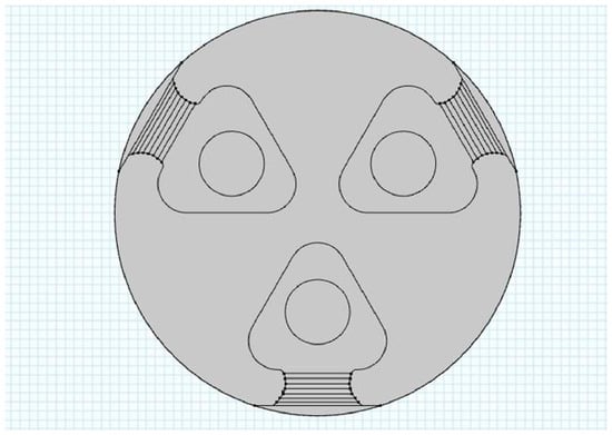
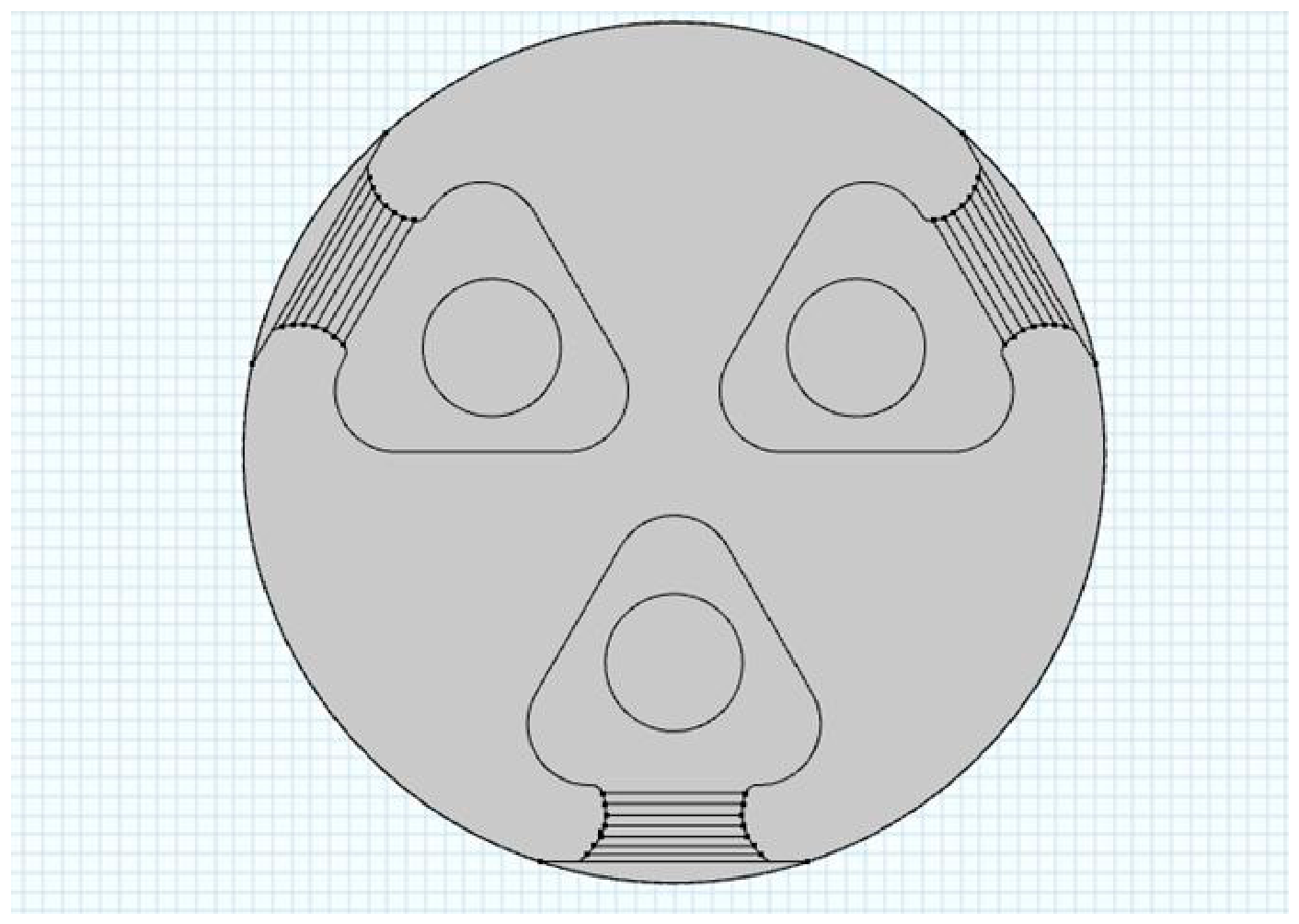
Figure 1 shows the delta-type spacer, which is surrounded by the green gas (g3) insulating medium. The spacer is round in shape and has three triangle-like sections arranged in a delta pattern. Each section has a hole in the centre to hold a conductor. This design keeps the conductors evenly spaced, provides mechanical support and helps prevent electrical problems such as flashover. The green gas surrounding the spacer replaces SF6 as the insulating medium and lowers the GWP of the busduct, while the FGM spacer provides the electrical and mechanical support.
Figure 1.
Delta-type spacer without metal insert (MI). The parallel lines in each leg mark the boundaries of the seven FGM grading layers.
In the FEM model, the region between the conductors, the spacer, and the enclosure is filled with g3 (4 mol% C4F7N/96 mol% CO2). In the electrostatic formulation of Section 2, the gas enters only through its relative permittivity, which was taken as εr = 1.0015. Because the relative permittivities of g3 and SF6 are both practically unity and far below that of the FGM spacer, the computed field distributions are governed by the spacer grading, the metal insert, and the defects, and would be practically the same for SF6. The influence of the green gas is therefore reflected in how the results are interpreted: the computed field stresses must be assessed against the lower withstand capability of g3 (about 25% lower than SF6 at the same pressure) and its higher sensitivity to defects.
The permittivity values in Table 1 were selected on the basis of three criteria. First, the lower limit, εr = 3.5, is the relative permittivity of unfilled cured epoxy resin at power frequency, so one end of each graded leg corresponds to the plain resin. The higher values are obtained by adding a high-permittivity inorganic filler to the same resin, which is the approach used to fabricate ε-FGM spacers in practice, with fillers such as Al2O3, TiO2, and SrTiO3. Second, the values are consistent with the ranges used in previous FGM spacer studies for three-phase GIB [22,23,24], which allows the results of the delta-type spacer to be compared with those of the post- and bulb-type spacers. Third, the three cases differ by a constant offset of 0.1 so that the sensitivity of the field stress to the overall permittivity level can be assessed while keeping the same grading profile.
The analysis of the delta-type spacer is next performed without and with the metal insert. The metal insert reduces the field stress and improves field uniformity near the enclosure end, as shown in Figure 2.
Figure 2.
Delta-type spacer with metal insert (MI). The parallel lines in each leg mark the boundaries of the seven FGM grading layers, and the MI (a thin ellipse combined with a rectangle) is embedded at the enclosure end of each leg.
The calculated electric field stresses without and with the metal insert are listed in Table 2 and Table 3, respectively.
Table 2.
Electric field stress of delta spacer without metal insert.
Table 3.
Electric field stress of delta-type spacer with metal insert.
The analysis of Table 2 and Table 3 reveals a significant reduction in electric field intensity at the enclosure when a metal insert is used in the delta-type spacer. For the R-phase conductor, the electric field stress decreased by approximately 24.65%.
In all cases, the R-phase leg shows a higher field stress than the Y- and B-phase legs; for example, at 72.5 kV the values in Table 2 are 0.0426, 0.0258, and 0.0248 kV/cm. This is a consequence of the boundary conditions, not of a physical difference between the phases. The electrostatic problem is solved at the instant when the R-phase voltage is at its positive peak, so VR = +Vm and VY = VB = −Vm/2 (Section 2). At this instant, the potential difference between conductor R and the earthed enclosure is twice that of conductors Y and B, so the field at the triple junctions of the R leg is the highest. The ratio of the R-leg field to the Y- and B-leg fields (about 1.65–1.72) is below 2 because the field near each leg is also influenced by the neighbouring conductors, between which the potential difference is 1.5 Vm. Conductors Y and B are at the same potential and are placed symmetrically about the axis of the R leg, so their field values should be equal; the small difference between them (about 4%) is attributed to the asymmetry of the finite-element mesh. At other instants of the cycle, the roles of the phases rotate, and by symmetry each leg reaches the same maximum field when its own conductor voltage is at its peak. The values reported for the R leg therefore represent the maximum field stress that any leg experiences during the power-frequency cycle, whereas the Y- and B-leg values correspond to the same instant and are not their own maxima.
3.1. Defect Modelling
Three defects that commonly arise during the manufacture, assembly, and ageing of cast-epoxy spacers are considered: a metallic protrusion, an internal void, and an interfacial delamination. Each defect is introduced only on the spacer leg supporting conductor B, at or near its enclosure-end triple junction, while the other two legs, the material grading and the boundary conditions are left unchanged so that the defect types can be compared directly. This location was chosen for three reasons: the field on the spacer is highest there; the triple junction is where surface flashover along solid spacers in compressed gas usually starts; and it is where the metal insert is placed, so the ability of the insert to mitigate defect-induced field enhancement is tested directly.
3.1.1. Protrusion
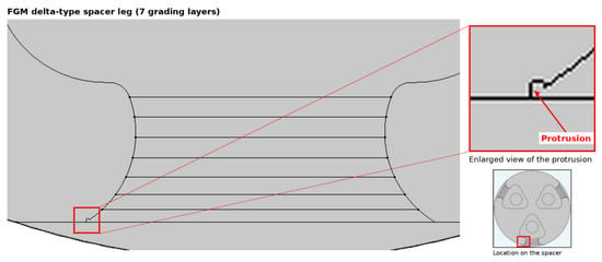
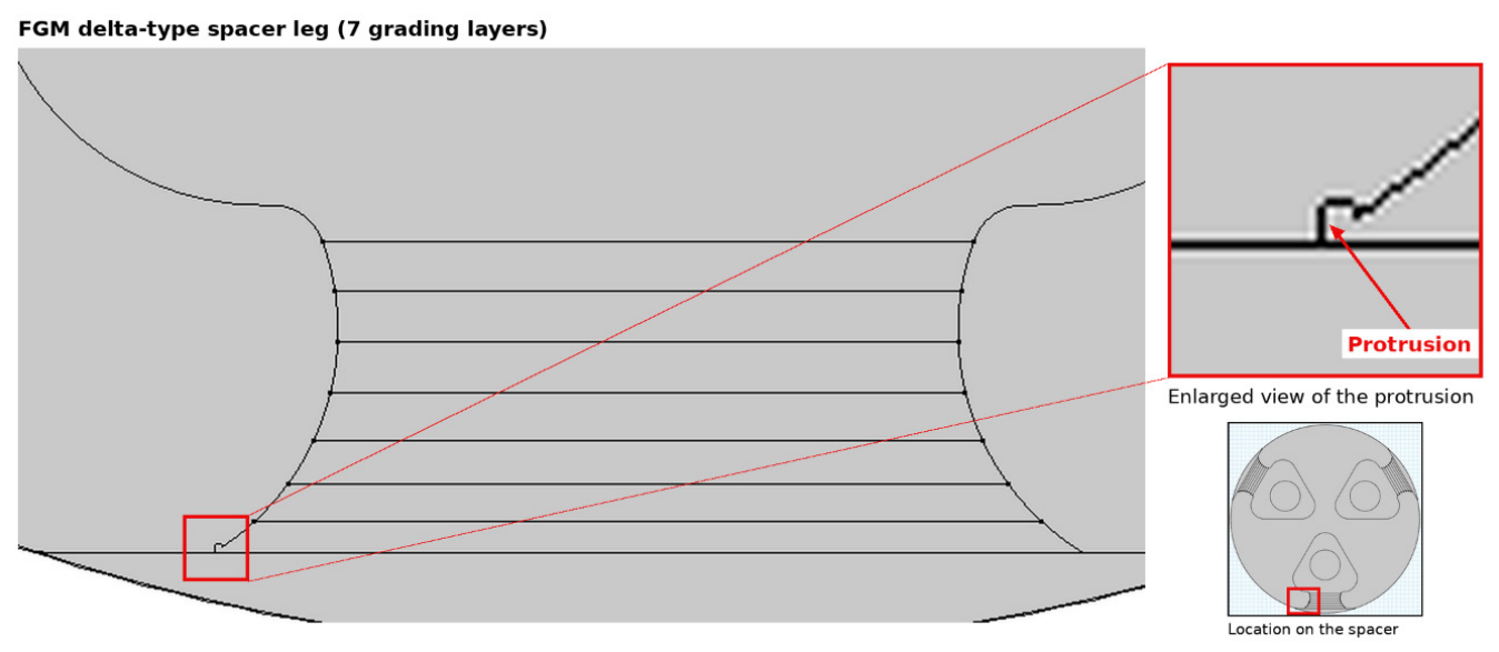
The field distribution at the spacer’s surface due to the protrusion defect can be analysed by this flaw at TJ. A metal insert of diverse forms and dimensions has been analysed to alleviate the effects of protrusion. An ideal metal insert, defined by a fusion of a rectangle and an ellipse, has been identified. The delta spacer with a protrusion defect is shown in Figure 3.
Figure 3.
Delta-type spacer with protrusion defect. The red box marks the protrusion, which is enlarged on the right; the small view below shows its location on the spacer.
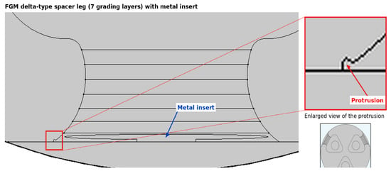
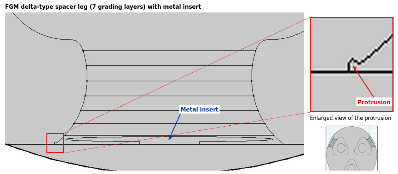
The rectangle has dimensions of 22 × 1.5 mm, whereas the ellipse possesses dimensions of 12.5 mm and 1.5 mm, respectively. This particular metal insert is engineered for incorporation at conductor B to attain optimal minimisation of the electric field. The field stress of the FGM spacer can be reduced by integrating a MI at the enclosing end of the spacer. The fabricated metal insert with the specified size is depicted in Figure 4.
Figure 4.
Delta-type spacer with protrusion and metal insert. The red box marks the protrusion, which is enlarged on the right; the small view below shows its location on the spacer.
3.1.2. Void
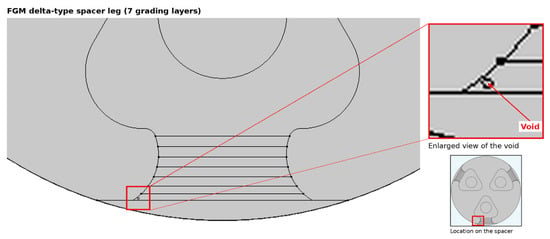
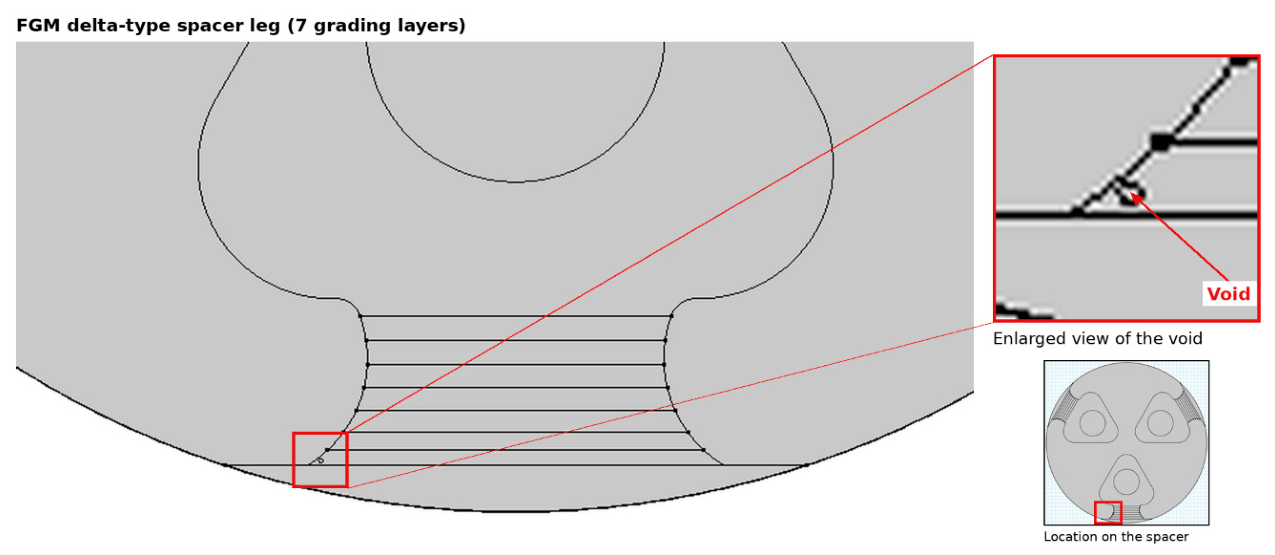
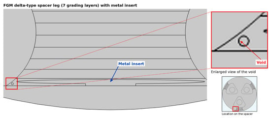
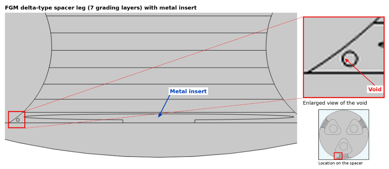
Figure 5 and Figure 6 depict the structural design of a delta-type spacer with a void region with and without MI, specifically focusing on the incorporation of a metal insert (MI) or the region where it may be placed or missing.
Figure 5.
Delta-type spacer with void. The red box marks the void, which is enlarged on the right; the small view below shows its location on the spacer.
Figure 6.
Delta-type spacer with void and metal insert. The red box marks the void, which is enlarged on the right; the small view below shows its location on the spacer.
3.1.3. Delamination
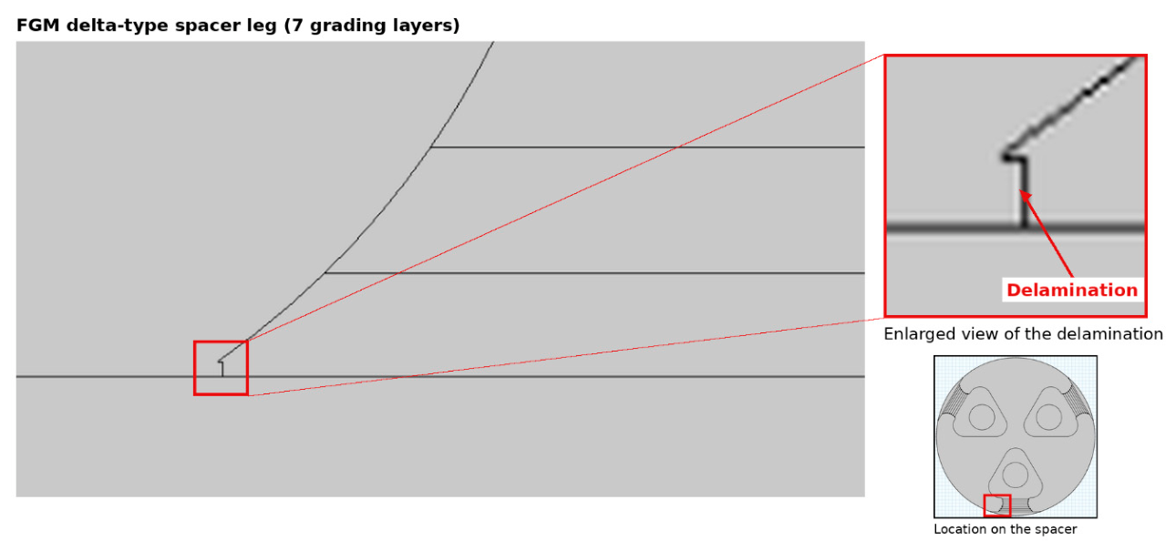
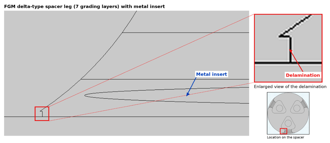
Figure 7 gives a closer look at this problem from the side, where you can clearly see gaps between the layers. This kind of damage weakens the spacer. Because the layers are not bonded well, the part cannot handle force as strongly as it should. Figure 7 and Figure 8 show a delta-type spacer with a problem called delamination with and without MI, which means the layers inside the material have started to separate.
Figure 7.
Delta-type spacer with delamination. The red box marks the delamination, which is enlarged on the right; the small view below shows its location on the spacer.
Figure 8.
Delta-type spacer with delamination and metal insert. The red box marks the delamination, which is enlarged on the right; the small view below shows its location on the spacer.
3.2. Defect Models: Types, Positions, and Sizes
Three defects that commonly arise during the manufacture, assembly, and ageing of cast epoxy spacers are considered: a protrusion, an internal void, and a delamination. Each defect is modelled on one spacer leg only, the leg supporting conductor B, while the other two legs are left defect-free. Their dimensions and positions are as follows: (i) Protrusion (Figure 3 and Figure 4): A sharp metallic protrusion of height 1.5 mm, width 22 mm, and tip radius 0.75 mm on the enclosure surface at the enclosure-end triple junction of the spacer leg, adjacent to the first grading layer. It represents a burr, a sharp machining edge or a metallic particle fixed to the enclosure near the spacer. (ii) Void (Figure 5 and Figure 6): A circular gas-filled cavity of diameter 2 mm inside the first grading layer, with its centre 2 mm from the enclosure and 2 mm from the spacer surface. It represents a gas bubble trapped in the resin during casting and curing. (iii) Delamination (Figure 7 and Figure 8): A gas-filled gap of length 10 mm and thickness 0.5 mm along the interface between the spacer and the enclosure, starting at the enclosure-end triple junction. It represents loss of adhesion at the interface caused by curing shrinkage or by thermal and mechanical cycling in service. For all three defect cases, the defect is introduced on the B-conductor spacer leg, while the remaining geometry, material grading, and electrical boundary conditions are kept unchanged to provide a consistent comparison of the effect of the different defect types.
All three defects are placed at or close to the enclosure-end triple junction of the spacer supporting conductor B for three reasons. First, the electric field on the spacer is highest in this region, as indicated by Table 2 and Table 3, making it the most electrically severe location for defect analysis. Second, the triple junction is a critical region for surface flashover initiation along solid spacers in compressed gas. Third, the metal insert investigated in this paper is positioned at the enclosure-end triple-junction region; therefore, placing the defects at this location directly evaluates the ability of the metal insert to mitigate the electric field enhancement caused by spacer defects.
The protrusion is modelled with a height of 1.5 mm, a width of 22 mm, and a tip radius of 0.75 mm; the internal void is represented by a circular gas-filled cavity of 2 mm diameter, located 2 mm from the enclosure and 2 mm from the spacer surface; and the delamination is represented by a gas-filled interfacial gap of 10 mm length and 0.5 mm thickness. These dimensions provide representative geometric models of metallic protrusion, internal void and interfacial delamination in cast epoxy insulation. The selected geometries reproduce the essential field-enhancement characteristics of each defect while maintaining a manageable computational model. A circular geometry is used for the void, a thin rectangular geometry for the delamination, and a sharp rounded-tip geometry for the protrusion. The defect dimensions are kept sufficiently small relative to the overall spacer and GIB dimensions so that the defects represent localised insulation imperfections. Only one size and one position of each defect are considered in the present study, while a detailed parametric investigation of defect size and position can be considered in future work.
4. Results and Discussion
4.1. Numerical Implementation and Simulation Conditions
The electrostatic problem was solved with the finite element package COMSOL Multiphysics using the AC/DC Module, Electrostatics interface. The geometry, material properties, boundary conditions, mesh generation, and post-processing were implemented in COMSOL. The stationary electrostatic problem was solved using a linear solver for the specified conductor voltages.
The model is the two-dimensional cross-section of a three-phase common-enclosure GIB with an enclosure outer radius of 225.5 mm and three conductors of radius 36 mm, placed 120° apart at 110 mm from the enclosure axis. Each leg of the delta-type spacer is divided into seven layers of equal length, each with the constant relative permittivity given in Table 1 for the grading type and case considered. The insulating gas is g3 with the relative permittivity given in Section 3. The metal inserts have the dimensions given in Section 3 and Section 4 and are bonded to the enclosure, so they are at earth potential. The defects (protrusion, void, and delamination) are modelled with the shapes and sizes shown in Figure 3, Figure 4, Figure 5, Figure 6, Figure 7 and Figure 8, with defect dimensions as specified in Section 3.2. The applied voltages are 72.5 kV, 220 kV, and 765 kV, line-to-line, r.m.s.; the conductor potentials are the instantaneous values defined in Section 2, and the enclosure is at zero potential. Because the earthed enclosure bounds the whole domain, no artificial outer boundary is needed.
The boundary conditions defined in Section 2 are summarised in Table 4, together with the conductor potentials applied for each system voltage.
Table 4.
Boundary conditions of the electrostatic model and conductor potentials for each system voltage, in kV (instant of R-phase positive peak; peak line-to-neutral values).
The properties of the g3 insulating gas used in the model and in the assessment of the results are summarised in Table 5.
Table 5.
Properties of the g3 insulating gas.
The following assumptions were made: (i) The problem is treated as two-dimensional and planar, i.e., the spacer is assumed to be long in the axial direction; the finite axial thickness of the spacer and three-dimensional end effects are neglected. (ii) The field is electrostatic: at power frequency the dimensions are negligible compared with the wavelength, and resistive (conduction) currents, space charge, and surface charge accumulation are neglected. The results therefore apply to AC operation and not to DC stress. (iii) All materials are linear, isotropic, and homogeneous within each region, with frequency- and temperature-independent permittivity; the continuous FGM grading is represented by seven discrete homogeneous layers. (iv) The defects are idealised geometric shapes, and all interfaces other than the delaminated one are assumed to be perfectly bonded. (v) The field is computed at a single instant of the three-phase voltage cycle, corresponding to the R-phase at its peak; other instants give different distributions.
The finite-element model employed quadratic Lagrange shape functions and contained 8090 elements, 986 boundary elements, and 114 vertex elements, with 16,319 degrees of freedom. The consequences of the previously reported delta type without a metal insert have produced increased intensity at TJs for all three conductors, R, Y, and B. The impact is alleviated by constructing a recessed MI with a 2D amalgamation of rectangular (18 × 4 mm) and elliptical (11 × 3 mm) geometries at the periphery of the delta-type FGM spacer, as depicted in Figure 2. A delta-type spacer composed of FGM is designed to establish a uniform electric field distribution, as depicted in Figure 1. Table 2 and Table 3 depict the electric field stress of functionally graded material (FGM) delta-type spacers without metal inserts at three different voltage levels—72.5 kV, 220 kV, and 765 kV—for various FGM types (GL-FGM, GH-FGM, and GU-FGM) under three permittivity conditions (C-1, C-2, and C-3). As expected, the electric field stress increases with voltage level across all configurations. At the highest voltage level (765 kV), a closer look reveals that GL-FGM shows a reduction in field stress as permittivity increases. Similarly, in the Y-phase, the reduction is from 0.2058 to 0.1993 kV/cm, equating to a 3.16%.
For the GL-FGM configuration, the field stress ranges from 0.0188 to 0.0406 kV/cm at V1, 0.0572 to 0.1231 kV/cm at V2, and 0.1406 to 0.3027 kV/cm at V3. The percentage change in field stress for GL-FGM at V1 is 115.96%.
In contrast, the GU-FGM configuration demonstrates the most uniform field distribution. The V1 values range from 0.0190 kV/cm to 0.0392 kV/cm (percentage change: 106.32%).
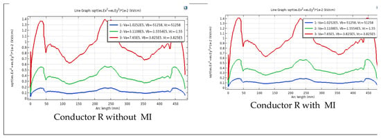
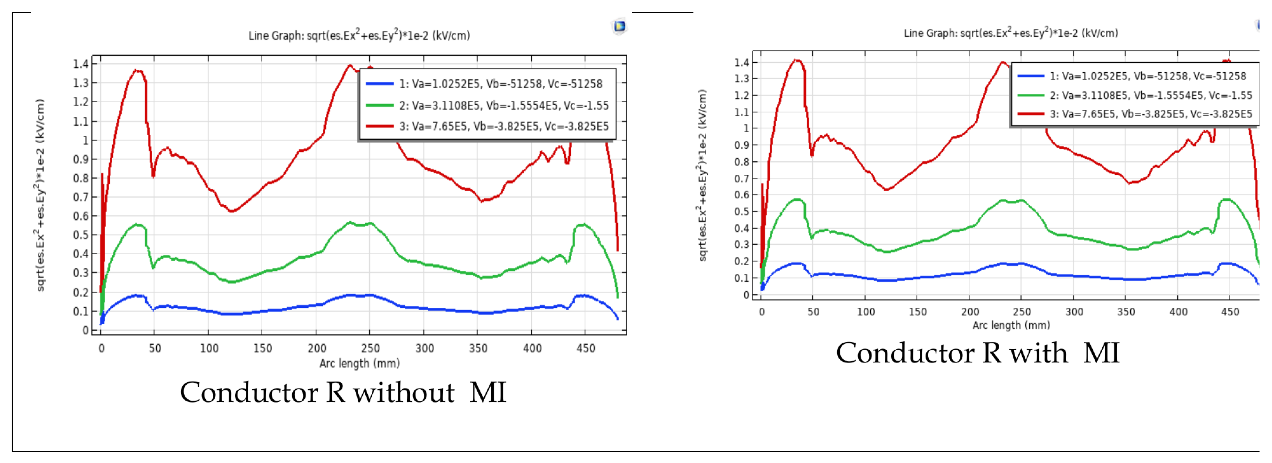
The R-phase electric field stress profiles without and with the metal insert are shown in Figure 9. The profiles correspond to the three investigated system voltage cases and show the reduction in stress near the enclosure-end region produced by the MI.
Figure 9.
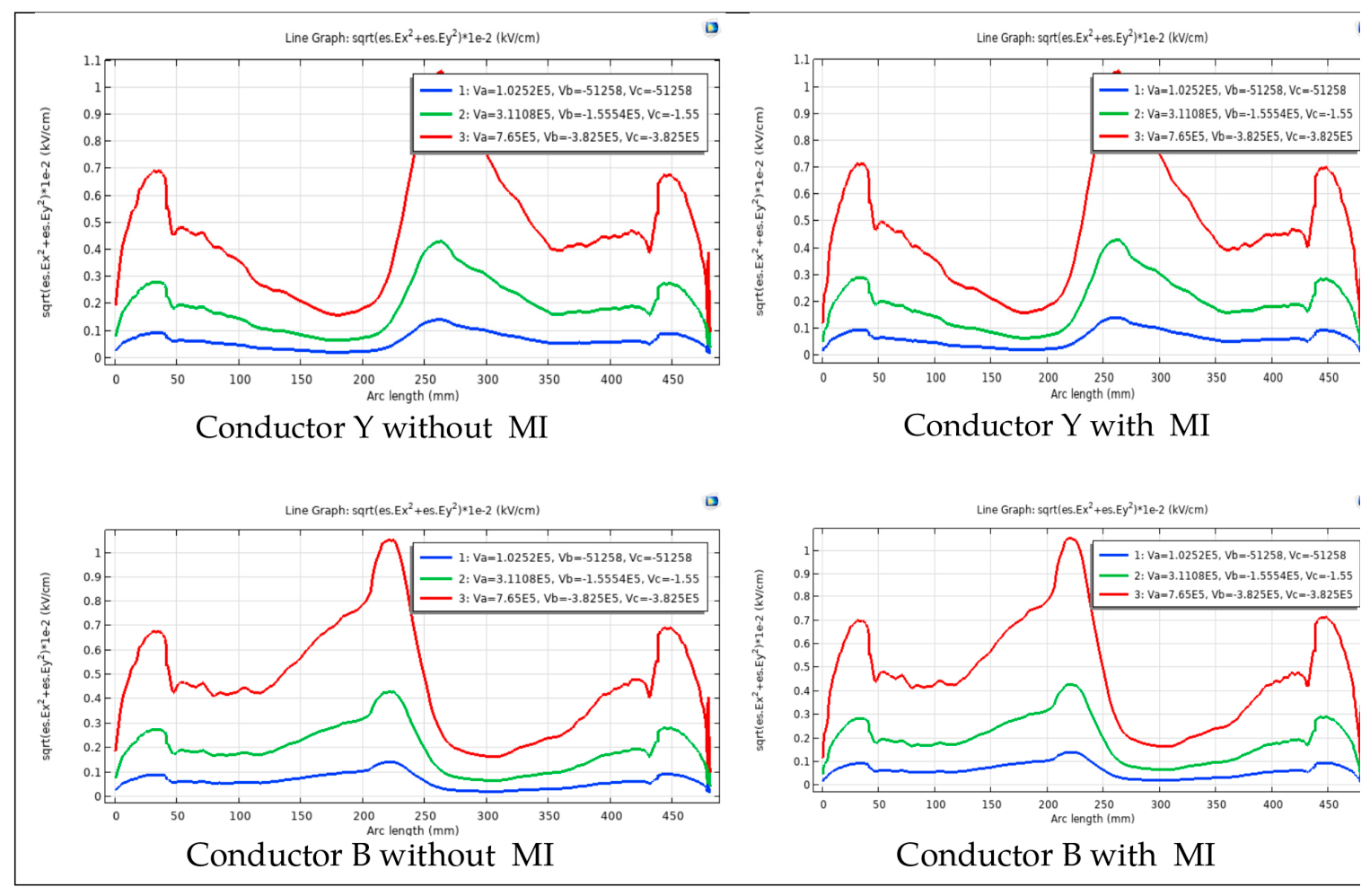
Electric field stress profiles for the R-phase conductor without and with the metal insert (MI) at the investigated voltage levels. In the legend, Va, Vb, and Vc are the potentials (V) of conductors R, Y, and B, respectively, for curves 1–3 (72.5, 220, and 765 kV systems). The vertical axis is the electric field magnitude, sqrt(Ex2 + Ey2) × 10−2 (kV/cm), and the horizontal axis is the arc length along the evaluation line. The same applies to Figure 10, Figure 11 and Figure 12.
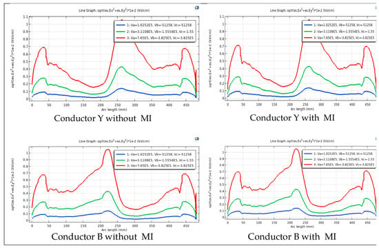
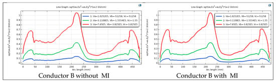
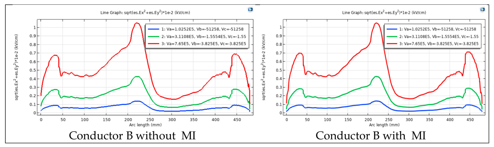
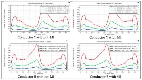
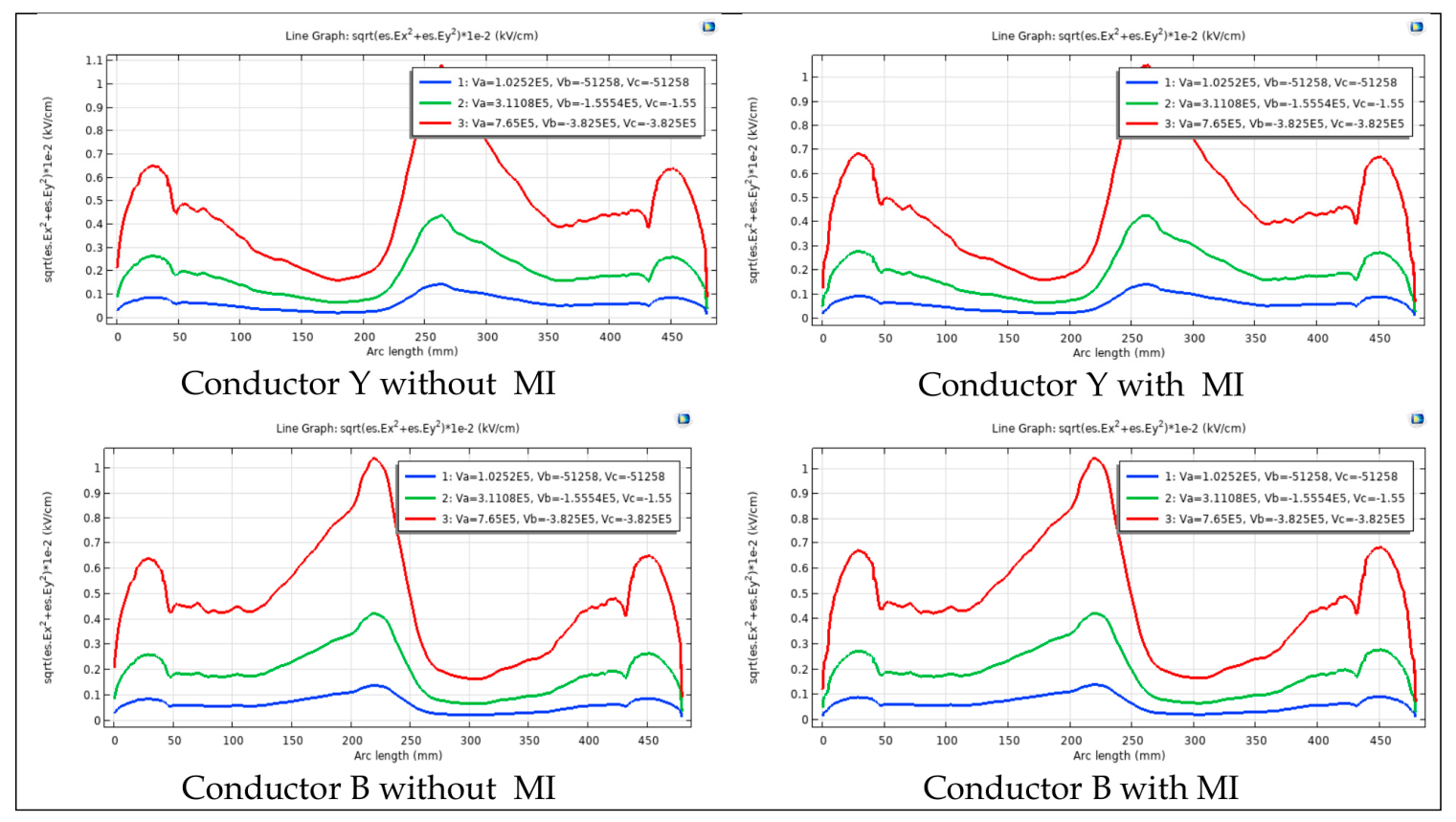
The electric field stress statistics for the protrusion, void, and delamination cases are shown in Figure 10, Figure 11 and Figure 12.
Figure 10.
Electric field stress statistics of conductors R, Y, and B for the delta-type spacer without and with MI under a protrusion defect.
Figure 11.
Electric field stress statistics of conductors R, Y, and B for the delta-type spacer without and with MI under a void defect.
Figure 12.
Electric field stress statistics of conductors R, Y, and B for the delta-type spacer without and with MI under a delamination defect.
The electric field stress variations in Figure 10, Figure 11 and Figure 12 are consistent with the tabulated results. The metal insert reduces the enclosure-end field stress, while the conductor-end stress remains practically unchanged.
A similar electric stress of 0.0258 kV/cm at V1, 0.0782 kV/cm at V2, and 0.1923 kV/cm at V3 is observed at the enclosure end of conductor-Y, as depicted in Table 2. The graph shows that for different operating voltages V1, V2, and V3, the electric stress at the enclosure end of conductor-B is 0.0248 kV/cm, 0.0752 kV/cm, and 0.1849 kV/cm, respectively. In order to minimise the failure of three-phase GIB, it is necessary to use an appropriate approach to lower the field stress that is created at the TJ of all three conductors. A metal insert of the appropriate size and shape inserted into the enclosing end of each of the three spacers will accomplish this. Data from Table 6, Table 7 and Table 8 show that field stress at enclosure ends of all conductors drops to the appropriate level with the MI, whereas the stress at the conductor ends is practically unchanged.
Table 6.
Comparative analysis of Estress for the 765 kV system, GL-FGM grading (50 Hz AC; 765 kV r.m.s. line-to-line; field at the R-phase positive peak).
Table 7.
Comparative analysis of Estress for the 765 kV system, GH-FGM grading (50 Hz AC; 765 kV r.m.s. line-to-line; field at the R-phase positive peak).
Table 8.
Comparative analysis of Estress for the 765 kV system, GU-FGM grading (50 Hz AC; 765 kV r.m.s. line-to-line; field at the R-phase positive peak).
All results in Table 2 and Table 3, and 6–8 are for alternating-current operation at the 50 Hz power frequency; no DC voltage is considered. The system voltages of 72.5, 220, and 765 kV are r.m.s. line-to-line values. Because the analysis is electrostatic (Section 2), the field is computed at one instant of the cycle, when the R-phase voltage is at its positive peak, and the reported stresses are therefore instantaneous peak values. The corresponding conductor potentials are listed in Table 4.
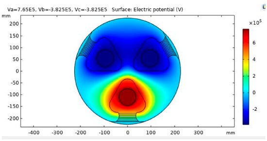
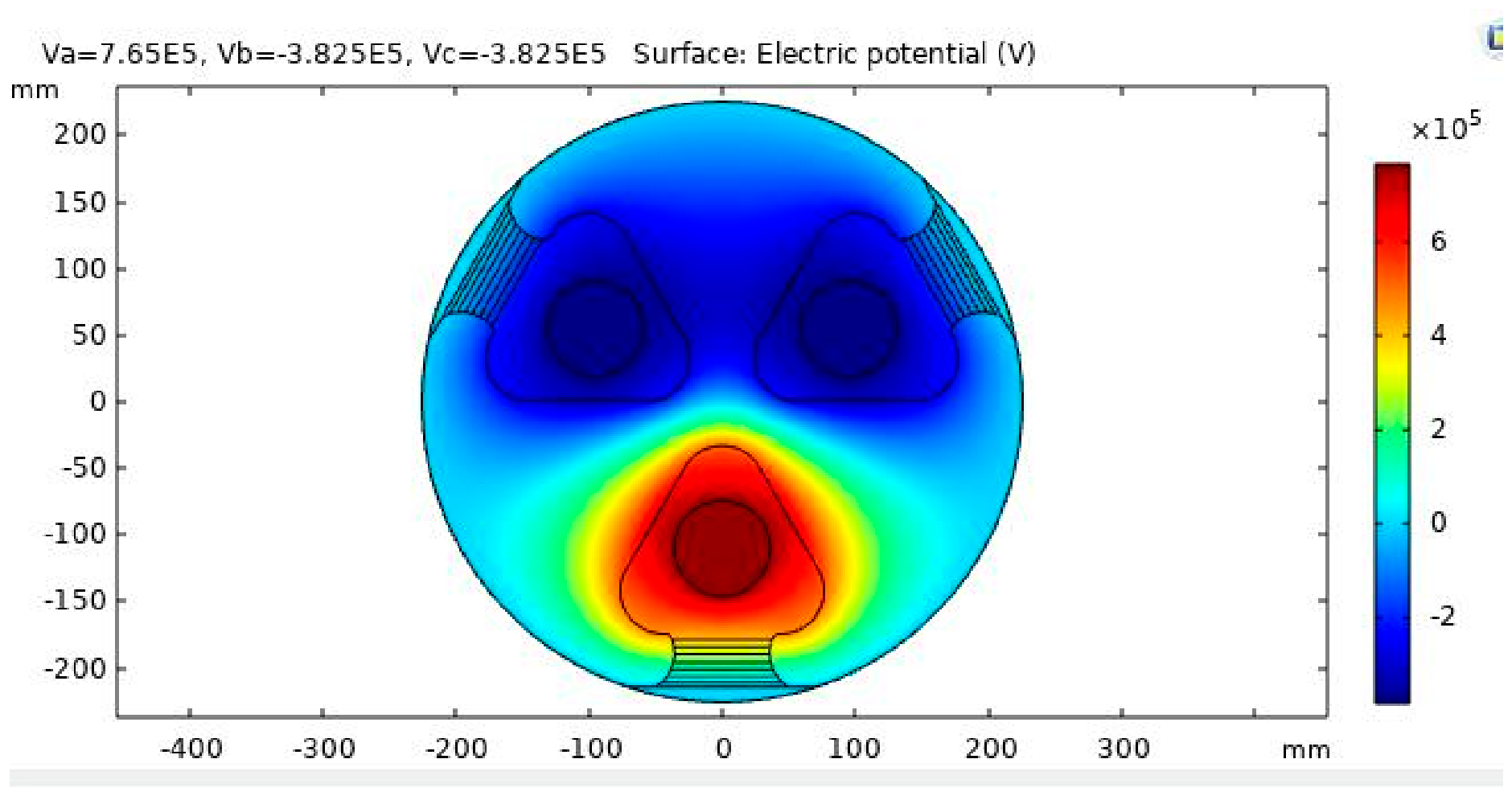
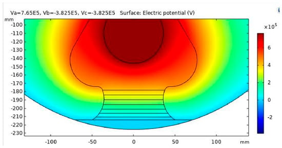
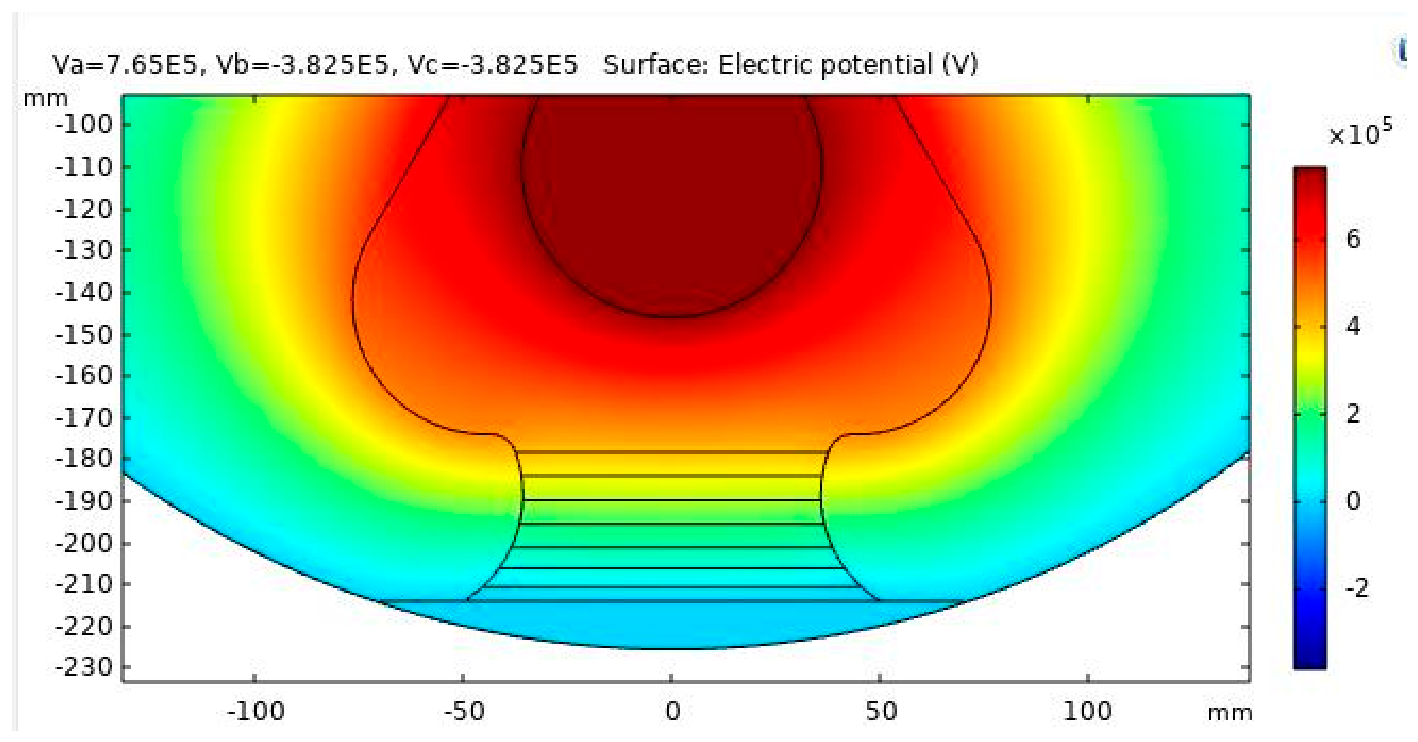
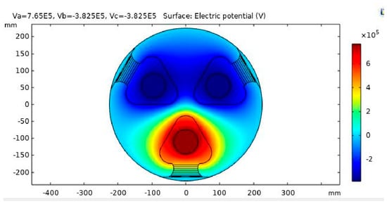
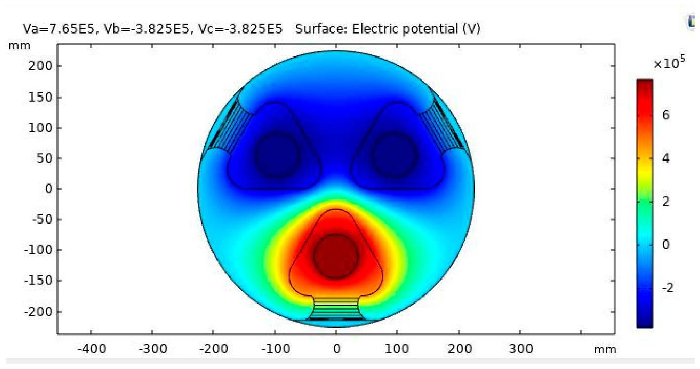
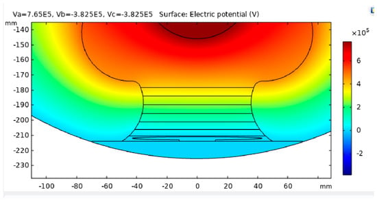
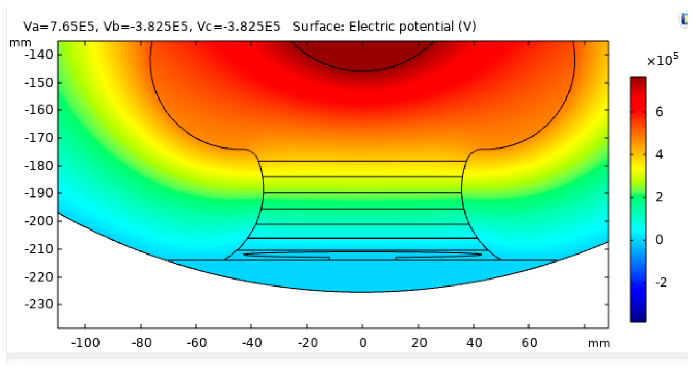
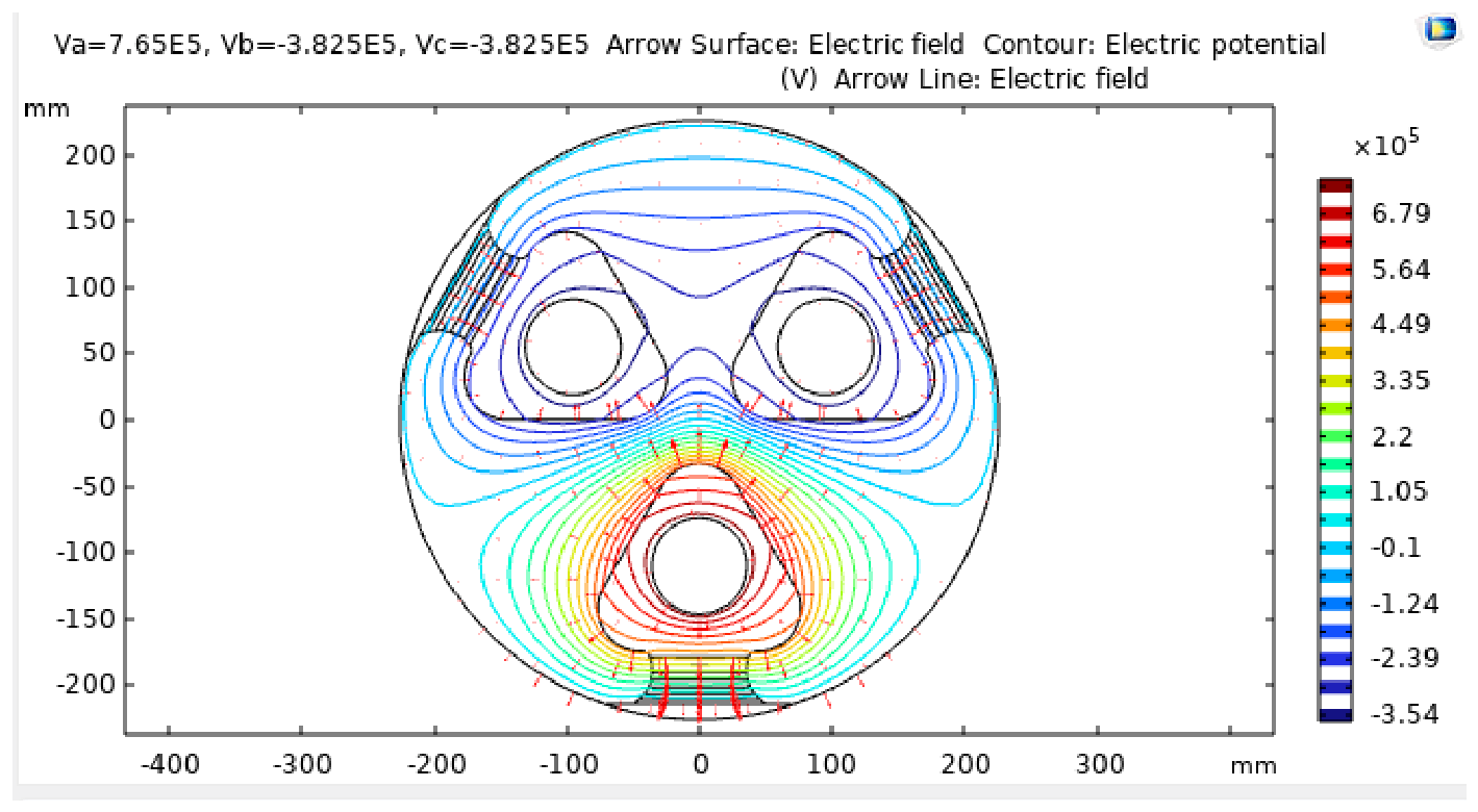
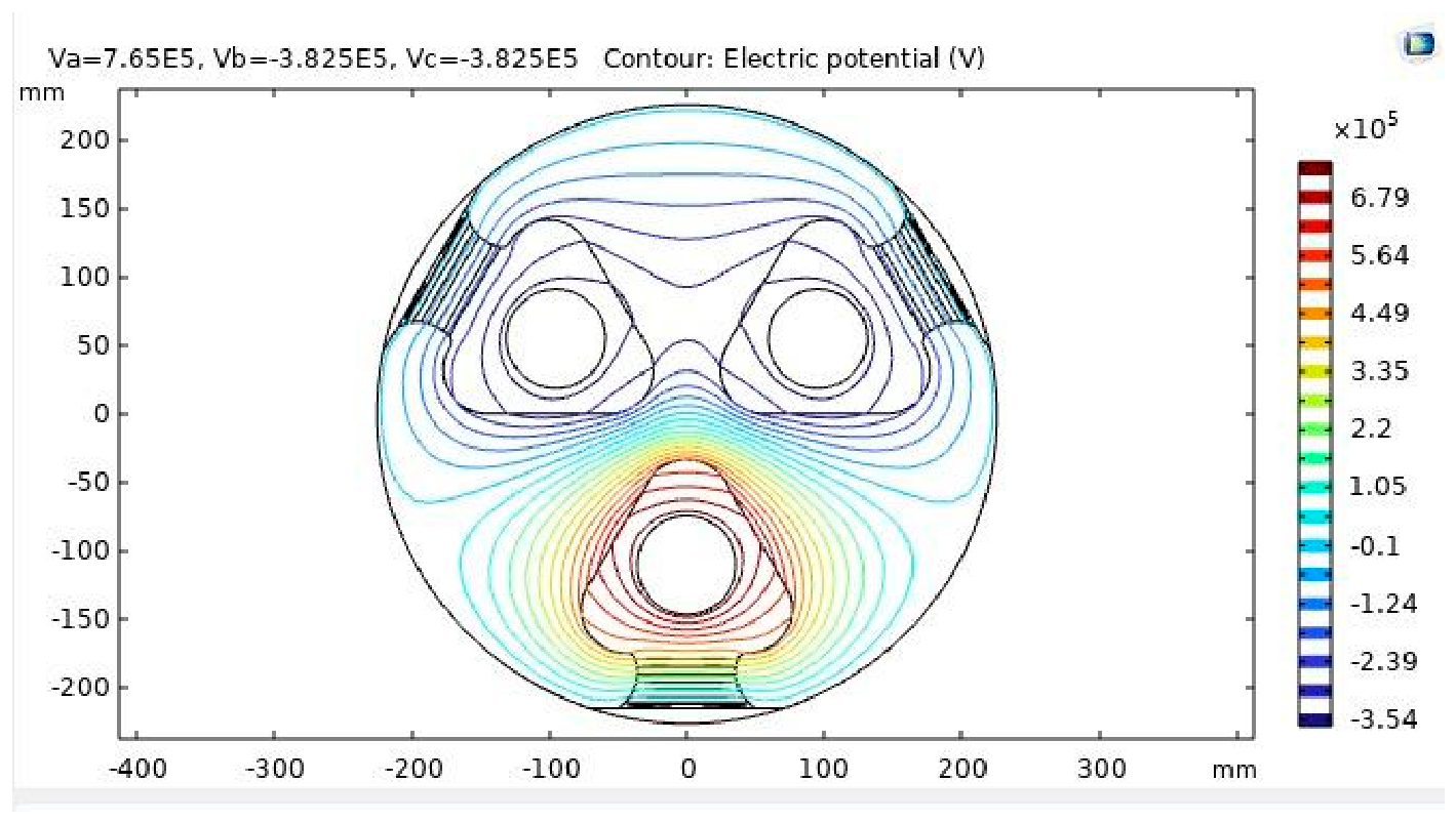
Figure 13, Figure 14, Figure 15, Figure 16, Figure 17, Figure 18, Figure 19 and Figure 20 show the computed solution for the defect-free FGM delta-type spacer in the 765 kV case, at the instant of the R-phase positive peak (VR = 765 kV, VY = VB = −382.5 kV, enclosure at 0 V). Figure 13, Figure 14, Figure 15 and Figure 16 are surface plots of the electric potential; Figure 17 and Figure 18 show equipotential contours, with the electric field vectors added in Figure 17, and Figure 19 and Figure 20 show the finite element mesh. Because the colour scale in Figure 13, Figure 14, Figure 15 and Figure 16 represents potential and not field strength, the highly stressed regions are those in which the colour changes most rapidly, i.e., where the equipotentials are most closely spaced.
Figure 13.
Electric potential distribution in the GIB cross-section with the FGM delta-type spacer without MI (765 kV case, instant of R-phase positive peak). In the plot header, Va, Vb, and Vc denote the potentials (V) of conductors R, Y, and B, and the colour bar gives the electric potential in V (×105). The same applies to Figure 14, Figure 15, Figure 16, Figure 17 and Figure 18.
Figure 14.
Enlarged view of the enclosure end of the R-phase spacer leg in Figure 13 (without MI).
Figure 15.
Electric potential distribution in the GIB cross-section with the FGM delta-type spacer with MI (765 kV case, instant of R-phase positive peak).
Figure 16.
Enlarged view of the enclosure end of the R-phase spacer leg in Figure 15 (with MI).
Figure 17.
Equipotential contours and electric field vectors (arrow length proportional to field strength) for the delta-type spacer without MI.
Figure 18.
Equipotential contours for the delta-type spacer with MI.
Figure 19.
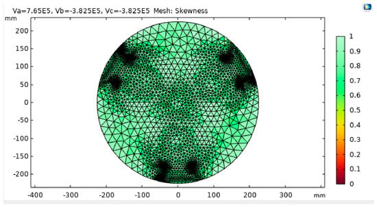
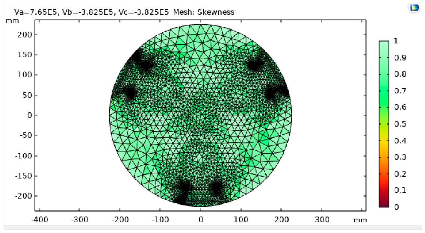
Finite element mesh, coloured by element skewness, for the delta-type spacer without MI.
Figure 20.
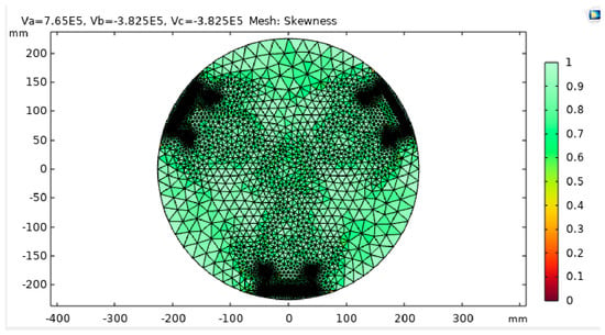
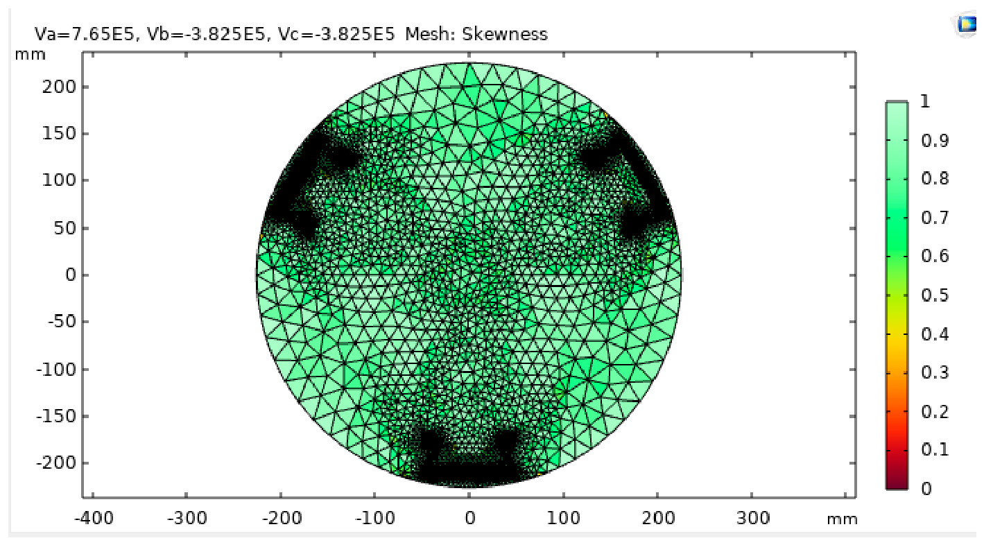
Finite element mesh, coloured by element skewness, for the delta-type spacer with MI.
In Figure 13, conductor R and its spacer leg appear dark red (+765 kV), conductors Y and B with their legs dark blue (−382.5 kV), and the earthed enclosure light blue (0 V). The potential inside each spacer bulb stays close to that of the conductor it surrounds: the epoxy has a permittivity about four times that of the gas, so little potential is dropped inside the bulb, and most of the conductor-to-enclosure potential difference is taken up across the graded neck of each leg and the adjacent gas. Between the phases, the potential passes through zero in the gas above the R leg, where the colour changes from red through green to blue over a short distance; this is the inter-phase region, across which the potential difference is 1.5 times the peak phase voltage. The distribution is symmetric about the vertical axis of the R leg, as expected from the equal potentials of conductors Y and B. Figure 15, with the MI, is practically indistinguishable from Figure 13 at this scale. The MI therefore does not alter the global potential distribution in the busduct, which is set by the conductor potentials and the geometry; its effect is confined to the enclosure end of each leg.
Figure 14 and Figure 16 enlarge the enclosure end of the R leg, which carries the highest stress. The seven graded layers appear as horizontal bands between the spacer bulb (top) and the enclosure (bottom). Across this neck, only about 35 mm high, the colour changes from orange, about 4 × 10⁵ V, at the uppermost layer to light blue at the enclosure, so a large part of the conductor-to-enclosure voltage is concentrated in the graded neck and in the gas beside its concave side surfaces. Inside the neck, the colour bands run almost parallel to the layer boundaries; the field is therefore directed mainly along the leg, normal to the layers, which is the orientation in which permittivity grading controls the field most effectively (Equation (14)). In Figure 16, the MI is visible as a thin ellipse combined with a rectangle, embedded at the bottom of the neck. Because the MI is earthed, its surface is held at 0 V: the lowest equipotentials terminate on the MI instead of on the enclosure, and the triple junctions at the two lower corners of the neck lie in the region shielded by the MI. This is the mechanism behind the lower enclosure-end stresses with the MI in Table 2 and Table 3.
Figure 17 combines the equipotential contours with arrows whose length is proportional to the local field. Around conductor R, the contours form closed, rounded-triangular loops that follow the outline of its spacer bulb, while around Y and B they form flatter loops; the zero-potential contour runs between the R leg and the Y and B legs. The contours are most closely spaced in two regions: across the graded neck of the R leg, between its bulb and the enclosure, and in the gas between the R bulb and the Y and B bulbs. The longest arrows appear at the enclosure end of the R leg, along both side surfaces of the neck and at its corners on the enclosure. This confirms that the enclosure-end triple junctions of the R leg are the most highly stressed locations in the cross-section, consistent with the R-leg values reported in Table 6, Table 7 and Table 8. The arrows point from conductor R towards the enclosure and towards Y and B, i.e., in the direction of decreasing potential. The closely packed contours at the necks of the Y and B legs show that their enclosure ends are also stressed, but less than that of the R leg at this instant.
Figure 18 shows the equipotential contours with the MI; no field arrows are plotted in this figure. Over most of the cross-section, the contour pattern is the same as in Figure 17, which again shows that the MI acts locally. The difference is at the bottom of each leg, where the lowest contours end on the MI rather than on the enclosure, moving the zero-potential surface away from the triple junctions.
Figure 19 and Figure 20 show the free triangular mesh without and with the MI, coloured by element skewness (1 for an ideal equilateral triangle, and 0 for a degenerate one). The element size varies from large elements in the open gas near the centre of the busduct to very small elements, which appear as dark clusters, at the enclosure ends of all three legs, where the thin graded layers, the curved side surfaces of the neck and the triple junctions must be resolved. Almost all elements have a skewness between about 0.6 and 1, indicating a good-quality mesh; the minimum element quality of 0.047 is confined to a few small elements at sharp geometric corners. With the MI (Figure 20), the refined region at the bottom of each leg extends across the whole width of the neck, because the thin MI geometry must be resolved by small elements; elsewhere the two meshes are practically identical. The mesh is a numerical discretisation and does not itself change the physical field: it follows geometry, and its fineness determines how accurately the local field peaks at the triple junctions are resolved.
4.2. Mesh Convergence Study
The solver residuals show that the finite-element equations were solved accurately on a given mesh, but not that the computed field stress is independent of the mesh. A mesh convergence study was therefore carried out for the 765 kV system with GL-FGM grading, permittivity case C-1, and the delamination defect, without the MI. The monitored quantity was the maximum field stress at the enclosure end of the R leg, the region of highest stress identified in Table 2 and Table 3. Three meshes, M1 to M3, were generated by reducing the maximum element size in the locally refined regions (triple junctions, gas–spacer interfaces, defects, and metal inserts) from 10.0 mm to 5.0 mm, by a factor of approximately 1.4 per step; this approximately doubled the number of elements at each step, while all other model settings were kept unchanged (Table 9). Mesh M3 (8090 elements and 16,319 degrees of freedom) is the mesh used for all results in this paper (Section 4.1). The ratio of degrees of freedom to elements is approximately 2.0 for every mesh, consistent with the quadratic Lagrange elements used.
Table 9.
Mesh convergence of the field stress at the enclosure end of the R leg (765 kV, GL-FGM case 1, and delamination defect, without MI).
The field stress increases monotonically from 0.1569 kV/cm on M1 to 0.1642 kV/cm on M2 and 0.1696 kV/cm on M3, i.e., by 0.0073 kV/cm (4.65%) and 0.0054 kV/cm (3.29%) for the two refinements. The M3 value is the one reported in Table 6 for the R leg, case C-1, delamination without MI. The decreasing change shows that the solution is converging, but slowly: the observed order of convergence is approximately 1.0, below the theoretical order of the quadratic elements. Because the same mesh settings were used for every configuration, a similar relative error is expected in each case, so the comparisons between configurations are less affected than the absolute values.
4.3. Comparison with the Dielectric Strength of g3
SF6 has long been the standard insulating gas in GIS and GIB, but it is a potent greenhouse gas. Its global warming potential (GWP) is 23,500 times that of CO2 over a 100-year horizon and its atmospheric lifetime is about 3200 years, so it is listed as a greenhouse gas under the Kyoto Protocol and the Paris Agreement [29]. Any SF6 released by leakage or during maintenance therefore contributes to global warming for centuries. The g3 mixture considered in this study has a GWP about 98% lower than that of SF6, and g3-insulated switchgear, transmission lines, and circuit breakers are already in commercial use [29]. Replacing SF6 with g3 therefore greatly reduces the environmental impact of the busduct, provided that the insulation design takes account of the lower dielectric strength of g3.
The purpose of the FGM grading and the MI is to keep the maximum field stress below the field that the g3 insulation can withstand. In a uniform or weakly non-uniform field, breakdown of an electronegative gas occurs when the field exceeds the critical value at which ionisation balances attachment; for SF6 the pressure-reduced critical field is (E/p)cr ≈ 89 kV/(cm·bar) [33]. At equal pressure, the dielectric strength of a 4 mol% g3 mixture is about 25% lower than that of SF6 [29], which is why g3 equipment is filled to a higher pressure. The maximum field stresses obtained with the two gases are therefore compared in Table 10.
Table 10 shows that the maximum field stress is almost the same with SF6 and g3. Without the MI, the values with g3 are 0.03–0.59% lower than with SF6, and with the MI they are 0.08–0.92% lower. This is expected, because both gases have a relative permittivity close to unity, so the electrostatic field distribution is determined mainly by the electrode geometry and the permittivity distribution of the FGM spacer rather than by the gas. Replacing SF6 with g3 therefore leaves the field stress on the spacer practically unchanged, but it lowers the field that the gas can withstand at a given pressure, which makes control of the local field stress more important.
The MI reduces the maximum field stress in all four cases and with both gases. With g3, the reduction is 17.98% for the defect-free spacer, 20.26% for the protrusion, 0.95% for the void, and 30.25% for the delamination; the corresponding reductions with SF6 are 17.94%, 19.98%, 1.36%, and 29.97%. The largest reductions occur for the delamination and the protrusion, which lie at the gas–spacer interface, where g3 is most sensitive to field enhancement. The small reduction for the void indicates that its local field is governed mainly by the permittivity contrast inside the spacer rather than by the electrode geometry. Combining FGM grading with the MI is therefore an effective means of reducing the field stress in defective spacers, so that the environmentally friendly g3 can replace SF6 without increasing the electrical stress on the spacer.
4.4. Limitations of the Idealised FGM and Defect Models
The results above were obtained with an idealised model: each spacer leg is graded in seven homogeneous layers with step changes in permittivity, the defects have regular shapes, and the interfaces carry no charge. Real FGM spacers and real defects depart from these assumptions in three ways, each of which limits how far the computed values can be transferred to a manufactured spacer.
Imperfect gradient transition. ε-FGM spacers are produced by casting epoxy with a spatially varying filler content, for example by centrifugal or layer-by-layer casting. The resulting permittivity profile is not a sequence of sharp steps: filler sedimentation and diffusion during curing smear each layer boundary over a finite width, the achieved values deviate from the target ones, and filler agglomeration causes local fluctuations. The smearing of the boundaries is the less important effect. Adjacent layers differ in εr by only 0.075 (GL, GH) or 0.15 (GU), so the jump in the normal field across a layer boundary, which by (14) equals the ratio of the two permittivities, is at most about 2% and 4%, respectively, and a continuous profile would change the triple-junction stress by a similarly small amount. Deviations of the overall permittivity level matter more. The three cases in Table 1 differ by a constant offset of 0.1 in εr (about 2.7%), and Table 6, Table 7 and Table 8 show that each such offset changes the 765 kV stress by up to 2.7%. A fabrication deviation of this size is therefore enough to mask the differences between the GL and GU gradings, which are below 0.8% for every conductor, defect and case. By contrast, the stress with GH grading is 3–14% higher than with GL grading, and the MI reduces the stress by 20–44% in all cases except the void on the R leg (1–2%); these differences are large enough to be expected to survive realistic manufacturing tolerances.
4.5. Interfacial and Surface Charge
The model imposes zero surface charge on every interface, Equation (14), so the grading acts purely capacitively. In a real graded spacer, each layer differs in conductivity as well as permittivity, and charge can accumulate at the layer boundaries (Maxwell–Wagner interfacial polarisation) and on the gas–spacer surface. Under 50 Hz AC, the interfacial charge in the bulk is small, because the charge-relaxation time of the epoxy layers, τ = ε0εr/σ, is of the order of 103 s for σ ≈ 10−14 S/m, far longer than the 20 ms period, so the charge cannot follow the alternating field. Charge supplied from the gas is a different matter. Near the protrusion and the delamination, the local field is enhanced; partial discharges in g3 start at only 76–84% of the inception voltage in SF6 [28], and the resulting charge can deposit on the spacer surface. Surface charge accumulation on epoxy insulators in C4F7N mixtures under AC has been measured [26], and on a tri-post insulator, it concentrates where the normal field is highest [25], i.e., in the regions identified as critical here. Such charge can raise or lower the field at the triple junction and is not represented in the present results. Under DC, under impulses superimposed on trapped charge, or after polarity reversal, the field is governed by the conductivity profile rather than the permittivity profile, and the conductivity of filled epoxy depends strongly on temperature, so a grading designed for AC permittivity control is not necessarily effective in those conditions [31]. The permittivity of filled epoxy also varies with frequency and temperature, which the constant values in Table 1 do not represent.
4.6. Idealised Defect Geometry
The void is a circle, the delamination a uniform rectangular gap and the protrusion a rounded tip of fixed radius (Figure 3, Figure 4, Figure 5, Figure 6, Figure 7 and Figure 8). Real defects are irregular, and the field enhancement they cause depends strongly on shape. For a gas cavity in a dielectric with εr ≈ 3.8 in a uniform field, the field inside a circular void in a two-dimensional model (i.e., a cylindrical cavity) is 2εr/(εr + 1) ≈ 1.6 times the surrounding field, that inside a spherical void is 3εr/(2εr + 1) ≈ 1.3 times, and that inside a thin flat void perpendicular to the field approaches εr ≈ 3.8 times. The two-dimensional model therefore overestimates the enhancement for a compact, near-spherical void but underestimates it for flat, crack-like voids, which are common in cast epoxy. Likewise, a real delamination tapers to zero thickness at its front instead of ending abruptly, which concentrates the field more than the uniform 0.5 mm gap, and real burrs and particles can have tip radii much smaller than 0.75 mm, with correspondingly higher local fields. The defects modelled here are thus representative rather than worst-case, and the field at the defect tips themselves is sensitive to the assumed radius and to the mesh refinement.
4.7. Implications
Because of these idealisations, the computed stresses should be read as comparative indicators for an ideal spacer under 50 Hz AC, not as absolute design values for a manufactured one. The conclusions that rest on large differences, namely, the reduction in the triple-junction stress by the MI and the higher stress with GH grading, are expected to hold for real spacers, whereas the small differences between GL and GU grading and between the permittivity cases cannot be resolved within manufacturing tolerances. Confirming the findings requires (i) a continuous permittivity profile measured on sectioned FGM samples, together with a statistical study of profile deviations; (ii) a coupled charge-transport model that includes the layer conductivities and surface charge; (iii) three-dimensional and parametric defect models; and (iv) experimental validation by partial-discharge, surface-potential, and flashover measurements on fabricated FGM delta-type spacers in g3.
5. Conclusions
This paper analysed, by two-dimensional electrostatic FEM, the field stress on an FGM delta-type spacer in a three-phase g3-insulated busduct for GL, GH, and GU gradings (cases C-1 to C-3), with protrusion, void, and delamination defects, without and with a recessed metal insert (MI). The main conclusions are as follows:
- (i)
- The MI is the most effective measure. It reduces the enclosure-end stress of the defect-free spacer by about 25% on the R leg and 39% on the Y and B legs and, with defects at 765 kV, by 20–44% in all cases except the void on the R leg (1–2%).
- (ii)
- The void is the most critical defect: it gives the highest R-leg stress for every grading, and the MI hardly reduces it.
- (iii)
- The GH-FGM configuration produces 3–14% higher electric field stress than GL-FGM in all investigated defect cases, suggesting that GL-FGM or GU-FGM may be preferable for reducing field stress. However, the differences should be interpreted in the context of numerical uncertainty, particularly for comparisons involving relatively small variations.
- (iv)
- Smaller differences are not resolved by the model. GL and GU differ by less than 0.8%, SF6 and g3 differ by less than 1%, and C-3 is 1.8–5.7% lower than C-1. These are comparable to the 3.3% change in the last mesh refinement and to permittivity tolerances in fabrication, so no GL/GU ranking is claimed, and the advantage of C-3 is indicative only.
- (v)
- The solver residuals confirm only the convergence of the linear solver. The mesh study shows the field still rising slightly with refinement (by 4.65% and 3.29%), so the reported values are slightly below the mesh-independent values and should be read as comparative indicators rather than absolute design values.
Since g3 has about 25% lower dielectric strength than SF6 and is more sensitive to protrusions, combining FGM grading with an MI is a promising approach for green gas busducts. Future work includes finer local meshing, three-dimensional and charge-transport models, and experimental validation.
Author Contributions
Conceptualisation, N.V.; methodology, N.V., V.N.K.G. and N.K.V.; software, N.V. and V.N.K.G.; formal analysis, N.V. and V.N.K.G.; investigation, N.V., V.N.K.G. and N.K.V.; validation, N.V., V.N.K.G. and N.K.V.; data curation, V.N.K.G.; supervision, V.N.K.G. and N.K.V.; writing—original draft preparation, N.V.; writing—review and editing, N.V., V.N.K.G. and N.K.V. All authors have read and agreed to the published version of the manuscript.
Funding
This research received no external funding.
Data Availability Statement
The data supporting the findings of this study are contained within the article.
Acknowledgments
APC funding for this open access article was provided by SRM University-AP under its Open Access Publishing Support Policy.
Conflicts of Interest
The authors declare no conflicts of interest.
References
- Li, D.; Zhang, G.; Wang, T. Characteristics of Surface Charge Accumulation on Truncated Cone-Type Spacer under AC Voltage. High Volt. Eng. 2022, 48, 1480–1488. [Google Scholar] [CrossRef]
- Yao, Y.; Wang, Z.; Chen, S.; Lin, X.; Cui, Z.; Zhang, H.; Geng, Z. Optimization Design of Insulating Spacer and Its Assembly Structure for 550 kV GIL. High Volt. Appar. 2021, 57, 50–57. [Google Scholar] [CrossRef]
- Li, J.; Wang, Y.; Dong, J.; Liang, H.; Du, B.; Xu, Y.; Li, X. Surface Charging Affecting Metal Particle Lifting Behaviors Around Epoxy Spacer of HVDC GIL/GIS. IEEE Trans. Dielectr. Electr. Insul. 2022, 29, 1546–1552. [Google Scholar] [CrossRef] [Scilit]
- Rachmawati; Kojima, H.; Kato, K.; Zebouchi, N.; Hayakawa, N. Electric Field Grading and Discharge Inception Voltage Improvement on HVDC GIS/GIL Spacer with Permittivity and Conductivity Graded Materials (ϵ/σ-FGM). IEEE Trans. Dielectr. Electr. Insul. 2022, 29, 1811–1817. [Google Scholar] [CrossRef] [Scilit]
- Dasgupta, S.; Baral, A.; Lahiri, A. Optimization of Electrode-Spacer Arrangement Using Simplex Algorithm. IEEE Trans. Dielectr. Electr. Insul. 2023, 30, 726–733. [Google Scholar] [CrossRef] [Scilit]
- Wang, C.; Li, W.; Chen, T.; Li, W.; Gong, R.; Zhang, G. Compact Design of 550 kV Basin-Type Spacer in Gas Insulated Switchgear (Part I)–Structure Optimization. Trans. China Electrotech. Soc. 2022, 37, 1847–1855. [Google Scholar] [CrossRef]
- Yao, H.; Du, B.X.; Li, J.; Wang, Y.H.; Liang, H.C.; Dong, J.N.; Zhang, C.; He, J.; Chen, R. Motion Behaviours of Metal Particle around SFGM Spacer under Non-Uniform Electric Field. In Proceedings of the 2020 IEEE International Conference on Applied Superconductivity and Electromagnetic Devices (ASEMD); IEEE: Piscataway, NJ, USA, 2020. [Google Scholar] [CrossRef] [Scilit]
- Xing, Y.; Sun, X.; Jiang, J.; Liang, F.; Liang, Z.; Zhuang, W.; Liu, B.; Li, D.; Cao, S.; Li, M.; et al. Significantly Suppressing Metal Particle-Induced Surface Charge Accumulation of Spacers in DC Gas-Insulated Power Transmission Lines. J. Phys. D. Appl. Phys. 2022, 55, 504003. [Google Scholar] [CrossRef] [Scilit]
- Li, J.; Wang, Y.; Chen, Y.; Liang, H.; Du, B.; Zhu, W. Design and Optimization of 1000 kV DC GIL Post Spacer with Surface Conductivity Gradient for ITER Neutral Beam Injector. In Proceedings of the 2020 IEEE International Conference on Applied Superconductivity and Electromagnetic Devices (ASEMD); IEEE: Piscataway, NJ, USA, 2020. [Google Scholar] [CrossRef] [Scilit]
- Wang, Y.; Li, J.; Xiao, M.; Liang, H.; Yao, H.; Du, B. The Improvement of Flashover Characteristics with Field Grading CCTO Coating for GIL Spacer. In Proceedings of the 3rd International Conference on Electrical Materials and Power Equipment (ICEMPE); IEEE: Piscataway, NJ, USA, 2021. [Google Scholar] [CrossRef] [Scilit]
- Hayakawa, N.; Kato, K.; Hikita, M.; Okubo, H.; Watanabe, K.; Adachi, K.; Okamoto, K. Development of Cone-Type FGM Spacer for Actual Size GIS. In Proceedings of the Annual Report Conference on Electrical Insulation and Dielectric Phenomena (CEIDP); IEEE: Piscataway, NJ, USA, 2020; pp. 255–258. [Google Scholar] [CrossRef] [Scilit]
- Kim, M.-S.; Hong, D.-S.; Cho, Y.-S.; Yun, C.-G.; Cho, H.-G. A Study on the Accelerated Life Models for Lifetime Prediction of the GIS Based on Insulation Spacer. In Proceedings of the 2022 6th International Conference on Electric Power Equipment–Switching Technology (ICEPE-ST); IEEE: Piscataway, NJ, USA, 2022; pp. 241–244. [Google Scholar] [CrossRef] [Scilit]
- Inoue, Y.; Kozako, M.; Hikita, M.; Masui, H.; Yanase, H.; Okamoto, K. Effects of Nano-Micro Composite and Shielding on Flashover Characteristics of Gas Insulated Switchgear Spacer Model in Different Lightning Impulse Application Methods. In Proceedings of the 2021 IEEE Conference on Electrical Insulation and Dielectric Phenomena (CEIDP); IEEE: Piscataway, NJ, USA, 2021; pp. 399–402. [Google Scholar] [CrossRef] [Scilit]
- Liang, H.; Du, B.; Kong, X.X. Basin-Type Spacer for DC-GIL–Part II: Surface Charge and Electric Field Regulation. IEEE Trans. Dielectr. Electr. Insul. 2022, 29, 1119–1126. [Google Scholar] [CrossRef] [Scilit]
- Zhao, C.; Tang, Z.; Zhang, L.; Wu, D.; Xia, H.; Li, H.; Pan, K. Entire Process of Surface Discharge of GIS Disc-Spacers under Constant AC Voltage. High Volt. 2020, 5, 591–597. [Google Scholar] [CrossRef] [Scilit]
- Zebouchi, N.; Haddad, M.A. A Review on Real-Size Epoxy Cast Resin Insulators for Compact High Voltage Direct Current Gas Insulated Switchgears (GIS) and Gas Insulated Transmission Lines (GIL)–Current Achievements and Envisaged Research and Development. Energies 2020, 13, 6416. [Google Scholar] [CrossRef] [Scilit]
- Fabio, M.R.; Hidayat, S.; Khayam, U. Effects of Notches in GIS Spacer Design to Hold Conductor Rods on Electric Field Distribution. In Proceedings of the 2021 3rd International Conference on High Voltage Engineering and Power Systems (ICHVEPS); IEEE: Piscataway, NJ, USA, 2021; pp. 241–246. [Google Scholar] [CrossRef] [Scilit]
- Sudarshan, T.S.; Dougal, R.A. Mechanisms of Surface Flashover along Solid Dielectrics in Compressed Gases: A Review. IEEE Trans. Electr. Insul. 1986, 21, 727–746. [Google Scholar] [CrossRef] [Scilit]
- Ueta, G.; Wada, J.; Okabe, S.; Miyashita, M.; Nishida, C.; Kamei, M. Insulation Performance of Three Types of Micro-Defects in Inner Epoxy Insulators. IEEE Trans. Dielectr. Electr. Insul. 2012, 19, 947–954. [Google Scholar] [CrossRef] [Scilit]
- Ueta, G.; Wada, J.; Okabe, S.; Miyashita, M.; Nishida, C.; Kamei, M. Insulation Characteristics of Epoxy Insulator with Internal Delamination-Shaped Micro-Defects. IEEE Trans. Dielectr. Electr. Insul. 2013, 20, 1851–1858. [Google Scholar] [CrossRef] [Scilit]
- Ueta, G.; Wada, J.; Okabe, S.; Miyashita, M.; Nishida, C.; Kamei, M. Insulation Characteristics of Epoxy Insulator with Internal Crack-Shaped Micro-Defects–Study on the Equivalence of Accelerated Degradation by Frequency Acceleration Test. IEEE Trans. Dielectr. Electr. Insul. 2014, 21, 1216–1225. [Google Scholar] [CrossRef] [Scilit]
- Subrahmanyam, K.V.; Rosalina, K.M. Reliability of FGM bulb type spacer in three-phase gas insulated busduct with protrusion and depression defects under particle contamination. Int. J. Syst. Assur. Eng. Manag. 2024, 15, 4540–4562. [Google Scholar] [CrossRef] [Scilit]
- Janaki, P.; Karthick, N.; Kumar, G.N. Design and analysis of FGM post type spacer in a three phase common enclosure gas insulated busduct under delamination. Electr. Power Syst. Res. 2021, 190, 106834. [Google Scholar] [CrossRef] [Scilit]
- Sobhan, P.V.S.; Pakalapati, J.; Gundavarapu, V.N.K.; Duvvada, D.C.; Bali, S.K. Electric field stress in a three phase common enclosure gas insulated busduct with FGM post type spacer and reduction with metal inserts. J. Electr. Eng. Technol. 2021, 16, 985–1002. [Google Scholar] [CrossRef] [Scilit]
- Li, X.; Zhang, F.; Yin, Y.; Wang, Y.; Huang, Q.; Li, Q. Multidimensional measurement method for surface charge on complex contoured surfaces of DC GIL tri-post insulator. In Proceedings of the 2nd International Conference on DC Technology Systems (DCTS); IEEE: Piscataway, NJ, USA, 2025. [Google Scholar] [CrossRef] [Scilit]
- Zhu, C.; Duan, X.; Li, S.; Guan, J.; Xin, Y.; Gao, Y. Effect of gas content on surface charge accumulation of epoxy insulator in C4F7N/CO2/O2 mixture under AC voltage. Energies 2025, 18, 4390. [Google Scholar] [CrossRef] [Scilit]
- Zhang, T.; He, F.; Chang, L.; Zhou, W. Study on dispersion of impulse discharge in SF6 and eco-friendly insulating gas C4F7N/CO2. Energies 2025, 18, 3228. [Google Scholar] [CrossRef] [Scilit]
- Wang, G.; Kim, W.-H.; Kil, G.-S.; Kim, S.-W.; Jung, J.-R. Green gas for a grid as an eco-friendly alternative insulation gas to SF6: From the perspective of partial discharge under AC. Appl. Sci. 2019, 9, 651. [Google Scholar] [CrossRef] [Scilit]
- Pan, B.; Wang, G.; Shi, H.; Shen, J.; Ji, H.-K.; Kil, G.-S. Green gas for grid as an eco-friendly alternative insulation gas to SF6: A review. Appl. Sci. 2020, 10, 2526. [Google Scholar] [CrossRef] [Scilit]
- Okamoto, K.; Hayakawa, N.; Kato, K.; Osawa, N.; Kozako, M.; Okubo, H. Enhancing Electrical Insulation Performance of Insulating Spacers using Functionally Graded Materials in Natural-Origin Gas GIS; CIGRE Session 2024, Paper No. 11054, Ref. D1-11054-2024; CIGRE: Paris, France, 2024. [Google Scholar]
- Liang, H.; Li, W.; Yao, H.; Du, B. DC/AC Electric Field Regulation by Functionally Graded Spacers Under Temperature Gradients. IET Sci. Meas. Technol. 2025, 19, e70037. [Google Scholar] [CrossRef] [Scilit]
- Yao, H.; Du, B.; Wang, Z.; Li, W.; Dong, J.; Liang, H. Research Progress on FGM for Epoxy Insulators in HV GIL/GIS. Chin. J. Electr. Eng. 2025, 11, 150–164. [Google Scholar] [CrossRef] [Scilit]
- Christophorou, L.G.; Olthoff, J.K. Electron Interactions with SF6. J. Phys. Chem. Ref. Data 2000, 29, 267–330. [Google Scholar] [CrossRef] [Scilit]

Disclaimer/Publisher’s Note: The statements, opinions and data contained in all publications are solely those of the individual author(s) and contributor(s) and not of MDPI and/or the editor(s). MDPI and/or the editor(s) disclaim responsibility for any injury to people or property resulting from any ideas, methods, instructions or products referred to in the content. |
© 2026 by the authors. Licensee MDPI, Basel, Switzerland. This article is an open access article distributed under the terms and conditions of the Creative Commons Attribution (CC BY) license.