


Abstract
The global expansion of interconnected edge network components requires immediate strategies for securing low-power computing nodes. Cryptographic algorithms executing over binary extension fields yield considerable computational benefits because their carry-free arithmetic significantly optimizes dynamic power consumption. However, general-purpose silicon architectures lack the dedicated hardware structures to run these finite-field operations efficiently, resulting in severe processing throughput bottlenecks. This study addresses this limitation by introducing a parallelized modular multiplier framework designed to integrate smoothly with the multicore execution environments of modern embedded platforms. Our approach deploys a progressive multiplier reduction (PMR) protocol that segments dense mathematical workloads into distributed structural thread groups. This architectural alignment allows multiplication matrices and spatial field reductions to take place concurrently, balancing localized workloads while decreasing intermediate data buffering demands. We present two distinct topological styles based on column division and row division techniques, deriving comprehensive analytical formulations to capture precise silicon area footprints, critical path delays, and total operational cycle counts. The resulting hardware metrics demonstrate that the parallel PMR design achieves a highly competitive area–delay product alongside optimized dynamic consumption characteristics. This structural paradigm delivers a scalable and robust security alternative for general edge hardware, ensuring system runtime stability while meeting tight environmental power constraints, protecting vital industrial assets, and sustaining emerging macroeconomic infrastructure.
1. Introduction
The contemporary trajectory of industrial modernization relies extensively on the deployment of autonomous embedded computing units across various global operations. Modern computing frameworks have transitioned past isolated microcontrollers into heavily integrated cyber–physical networks that regulate automated factory-floor production lines, manage smart electrical utility grids, and monitor complex logistics tracking nodes. This widespread technological transition aligns directly with international development goals, mapping explicitly to UN Sustainable Development Goal 9, which focuses on building resilient, ecologically efficient industrial infrastructure. The systemic integration of these automated nodes also supports UN Sustainable Development Goal 8, which promotes sustained economic growth by ensuring the safety and operational continuity of digital workflows powering modern commerce. However, because these versatile edge processors depend on distributed wireless channels to broadcast runtime telemetry or accept operational commands, they introduce an exposed and vulnerable surface to sophisticated cyber-adversaries. Unauthorized access or data manipulation within these critical industrial systems can trigger severe financial data theft, corporate exploitation, or catastrophic infrastructure failures that directly destabilize national economic frameworks.
Establishing dependable data protection within these exposed frameworks requires the implementation of robust, high-grade cryptographic protocols. Public-key elliptic-curve cryptography (ECC) configurations supply vital encryption and key-exchange layers, while symmetric ciphers like the Advanced Encryption Standard (AES) provide efficient data validation and blocks for firmware authentication. These mathematical tools collectively guarantee data confidentiality, information integrity, and system node verification across decentralized operating networks. Even so, embedding these computationally demanding protocols directly into edge nodes presents serious engineering challenges due to the stark physical limitations of embedded hardware. These modules are forced to operate under extremely strict thermal and power envelopes, possess limited silicon area budgets, and demand completely deterministic, low-latency execution boundaries to prevent delaying real-time automation feedback loops. Standard software routines handling these complex algebraic formulae are fundamentally insufficient for long-term standalone use, as they lack the raw arithmetic throughput and energy management required for autonomous field applications.
To circumvent these operational bottlenecks, deploying specialized hardware accelerators focused entirely on modular multiplication—the most resource-demanding arithmetic foundation of public-key engines—has become critical [1]. Within elliptic curve mathematics, modular multiplication serves as the core computational layer driving point additions and point doublings, which together dictate the overall performance of digital signature generation and verification. Designing efficient cryptographic hardware requires an optimized mathematical approach, which is why modern implementations rely heavily on the unique characteristics of the binary extension field . In contrast to traditional prime-field () environments—where integer operations trigger long, power-hungry carry propagation paths that degrade clock speed—arithmetic execution inside is inherently carry-free [2,3]. Additions are resolved via simple parallel XOR gates, completely preventing carry delays, reducing the underlying silicon footprint, and making binary fields highly advantageous for edge hardware relying on battery cells or environmental energy harvesting.
The physical efficiency of a mathematical engine depends entirely on the chosen Polynomial Basis and the structural parameters of the irreducible field equation. While implementations utilizing Normal Basis (NB) or Redundant Basis (RB) formats can offer select operational advantages, Polynomial Basis (PB) formulations remain highly popular for general silicon execution due to their structural simplicity, predictable routing paths, and the complete elimination of complex basis-conversion processing blocks [4,5,6,7]. Furthermore, field characteristics are heavily driven by the shape of the primitive polynomial; though trinomial and pentanomial configurations are widely selected to reduce gate counts, All-One Polynomial (AOP) architectures provide highly effective alternatives for specialized arithmetic structures [8,9]. Despite these clear field-level advantages, traditional general-purpose multicore microprocessors are structurally unsuited to run operations because their Arithmetic Logic Units (ALUs) are explicitly wired for standard integer and fixed-point data formats. A standard processor’s internal adder uses chained full-adder arrays to handle carries, and its multiplication units are designed for integer products using carry-save arrays. Standard commercial microcontrollers are confined to basic bitwise operations that fail to scale efficiently when managing high-security field lengths such as or [10,11]. Conversely, specialized cryptographic coprocessors or Hardware Security Modules (HSMs) are custom-engineered to execute multi-field operations over , , and various post-quantum polynomial rings for post-quantum security [12]. These specialized architectures deploy highly parallelized XOR logic matrices and leverage dedicated systolic array accelerators to maximize processing concurrency while maintaining a highly restrictive power profile.
Historically, many dedicated cryptographic processors were engineered through empirical, intuitive techniques that fell short of the strict optimization demands imposed by modern parallel embedded systems. In contrast to these informal paradigms, rigorous analytical design methods empower engineers to systematically regulate execution concurrency, intercore data exchange, and processing element workloads [13]. Prior frameworks heavily relied on algorithmic dependence graphs to capture localized interactions between data variables. Although instrumental for baseline synthesis, such representations constrained the comprehensive exploration of underlying hardware design spaces. To address these limitations, a variety of architectural enhancements have emerged, including fault-detecting array configurations [14], consolidated multiplication-and-squaring blocks [15], and localized-communication Montgomery engines optimized for resource-constrained IoT applications [16,17]. Moreover, sophisticated multi-dimensional scheduling and task-mapping strategies have been developed to manage operand word lengths and interconnection overheads in structures operating over trinomial-generated fields.
While modern multicore architectures leverage spatial parallelism to bypass traditional power limitations, they introduce significant problems concerning workload balancing and inter-processor communication (IPC). In highly sensitive real-time edge nodes, dividing massive cryptographic data words across disconnected processor cores can cause routing congestion and high signal-switching activity, which rapidly exhausts limited energy reserves. Many existing parallel systolic systems are hindered by high communication-to-computation ratios, as their field-reduction stages demand continuous data shuffling across processor boundaries to resolve feedback terms. This communication bottleneck can introduce unpredictable operational latencies that disrupt sensitive real-time industrial control loops.
To solve these intercore communication issues, this paper introduces a parallelized modular multiplication framework engineered to optimize the structural match between finite-field arithmetic and the multicore layouts of modern embedded systems. Moving past traditional single-core layouts, our approach utilizes a multicore execution grid to run a progressive multiplier reduction (PMR) algorithm, drawing structural design paradigms from previous product reduction formulations. This scheme structures the overall workload by dividing computations across localized blocks of rows or columns. This targeted distribution localizes intermediate data feedback within individual processing cores, drastically lowering cross-core communication traffic and establishing uniform processor utilization compared to classic “multiply-then-reduce” hardware pipelines. This research presents a rigorous architectural evaluation platform by investigating two distinct multicore mapping strategies: progressive multiplier reduction with column division (PMR-CD) and progressive multiplier reduction with row division (PMR-RD). Utilizing formal analytical derivations, we establish explicit hardware complexity models that quantify overall silicon area, critical path propagation delays, and total clock cycle periods as functions of parallel processor scaling. A primary finding from this structural exploration indicates that the PMR-RD topology exhibits enhanced energy efficiency, characterized by a monotonically decreasing area–delay product (ADP) as a larger number of computing cores are deployed within the processing array. By validating these specialized hardware configurations, this work delivers a highly scalable, low-complexity cryptographic engine well suited for general-purpose embedded systems, thereby securing edge network nodes while sustaining strict power budgets and deterministic runtime execution profiles.
The remainder of this manuscript is structured as follows: Section 2 reviews the foundational concepts of finite-field arithmetic required for developing the PMR method. Section 3 establishes the core mathematical formulations for the progressive multiplier reduction algorithm developed in this work. Section 4 introduces the task partitioning strategies and the baseline architectures for multicore mapping. Section 5 develops the parallel progressive multiplier reduction algorithm using the column division technique (PMR-CD). Section 6 details the design and coordination layout of the proposed row division paradigm (PMR-RD). Section 7 explores the hardware mapping configurations and parallel execution modes evaluated across the multicore processing architecture. Section 8 derives analytical formulations to estimate the physical area and critical path delays of the multicore system; this section also evaluates the exact number of clock cycles required to complete the baseline and proposed parallel implementations. Section 9 analyzes the performance metrics by comparing consumed area, execution delays, and area–delay product optimization trends. Finally, Section 10 summarizes the major research findings, concludes the study, and identifies target areas for future exploration.
2. Mathematical Background for Modular Multiplication Algorithm
In this section, we delineate the essential mathematical principles governing the binary extension field that serve as the groundwork for establishing our progressive multiplier reduction scheme, alongside evaluating the performance metrics of the proposed algorithm implementations. Throughout this analysis, the field is constructed via an irreducible primitive polynomial of degree m, expressed as follows:
where .
To confirm the universal applicability of this construction across any degree m, we recall that a primitive polynomial of degree m is characterized by the existence of a primitive root whose multiplicative order satisfies [18,19,20,21]
The total number t of such valid primitive polynomials of degree m is formally determined by
where denotes Euler’s totient function. Because for all , t is guaranteed to be a positive integer, thereby proving that valid primitive polynomials exist for any choice of m. Crucially, these defining field polynomials are not restricted to sparse structures such as trinomials or pentanomials but encompass any valid term distribution.
Based on this general formulation, applying the fundamental reduction identity
directly yields the generalized substitution relation:
To demonstrate how this reduction rule operates directly on field elements, consider an unreduced polynomial whose leading term has reached degree m:
Under modulo-2 addition, can be reduced to its congruent field representation in by adding the zero-equivalent field polynomial :
This explicit cancellation validates the primary reduction substitution rule implemented throughout our hardware framework:
Building upon this basic substitution, the following lemma defines the exact structural conditions under which a higher-degree polynomial () can be fully reduced in a single parallel iteration, versus when the reduction cascade requires additional computational cycles:
Lemma 1.
Given the polynomial
where
and , it is possible to reduce in one step.
Proof.
We can write as
Using Equation (8), we can write
To perform the single-step reduction of , the upper bound on the degree of the resulting polynomial must comply with the following inequality:
which is the desired result. □
The reduction operations in Lemma 1 apply to one-term . The following lemma shows how a short polynomial with degree can be reduced in one step:
Lemma 2.
Considering a polynomial of degree d, which is expressed as
where Z denotes the total number of terms in , a single-step reduction of is achievable under the condition that
Proof.
Substituting the result of Lemma 1 into Equation (11) allows the term to be replaced by :
Because the degree of is , this polynomial multiplication can be completed in a single step provided that the degree of complies with the inequality
or
□
3. Progressive Multiplier Reduction (PMR) Derivation
Consider two polynomials :
The product of the two in terms of PMR is expressed as
Equation (16) is an unconditional shift-and-reduce operation. On the other hand, Equation (17) is a conditional add–multiply. This is a feature commonly encountered in many cryptographic algorithms such as Rivest–Shamir–Adleman (RSA) and elliptic-curve cryptography (ECC).
We can express the iteration in Equation (16) explicitly as
such that the degree of the simplified multiplier polynomial is strictly bounded below m.
The progressive multiplier reduction (PMR) modular multiplication process is detailed in Table 1, where each horizontal row corresponds to the generation of an individual partial product component. This specific illustration is provided for a field dimension of .
Table 1.
Operational breakdown of the PMR modular multiplication method for , where every sequential row denotes a computed partial product.
We can express the iterations in Equations (16) and (17) in a bitwise fashion as follows:
where the indices have the ranges and .
The iterations in Equations (21) and (22) correspond to a regular iterative expression that can be implemented as a hardware systolic array or as a software multithreaded system using formal techniques explained in [22].
3.1. Study of Algorithm Variables
An iterative procedure governed by two distinct indices, i and j, is formulated in Equations (20)–(23). Because these indices are restricted to positive integer values, the corresponding iterations span a two-dimensional (2D) convex domain denoted as [22]. This algorithm operates on the input multiplier polynomials A and B, alongside the updated intermediate polynomial and the evolving partial product polynomial . The final output yielded by this process is the modular product polynomial P.
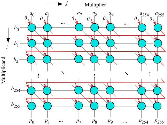
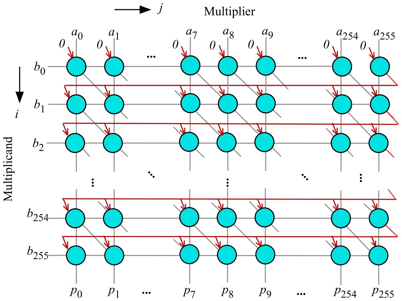
The iteration dependence graph (DG) for a field size of is illustrated in Figure 1. For this graphical representation, a degree-256 primitive trinomial is assumed with the structural form
where the degree of is less than m and the nonzero coefficients depend on which is chosen.
The intermediate polynomial bits are updated according to Equations (21) and (22). This is shown by the diagonal lines in Figure 1 as well as the red lines due to the reduction operation. The input multiplicand B bits depend only on the index i. Therefore, these bits are represented by the horizontal lines in Figure 1. The intermediate product polynomial is updated according to Equation (22). This is shown by the vertical lines in Figure 1.
3.2. Word-Level Standard PMR Formulation
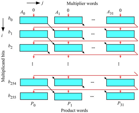
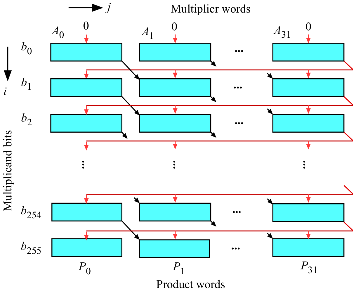
The dependency structure governing the conventional word-level PMR technique is illustrated in Figure 2. To facilitate execution on processors that operate natively on multi-bit data blocks rather than individual bits, the multiplier operand (A) is partitioned into distinct words of size W bits. For demonstration purposes, the figure depicts an architectural instance where , , and . The red arrows show the coefficients of . Some of those are zero, depending on which is chosen. The total count of multiplier words, denoted by L, is computed as follows:
Figure 2.
Classic word-based PMR algorithm DG. Case when , , and . The red arrows show the coefficients of . Some of those are zero, depending on which is chosen.
To guarantee that the field dimension m is a strict integer multiple of the word length W, the most significant bit positions of m can be padded with zero-valued words.
The multiplier polynomials are expressed in words in the following form:
The product is given by
4. Proposed Embedded Multicore PMR Algorithm
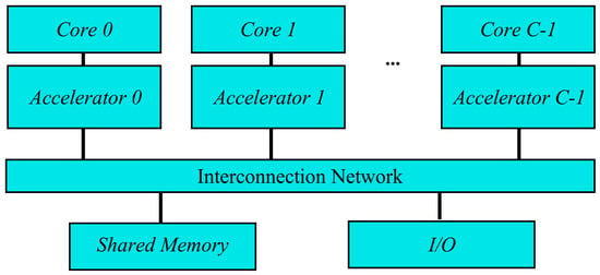
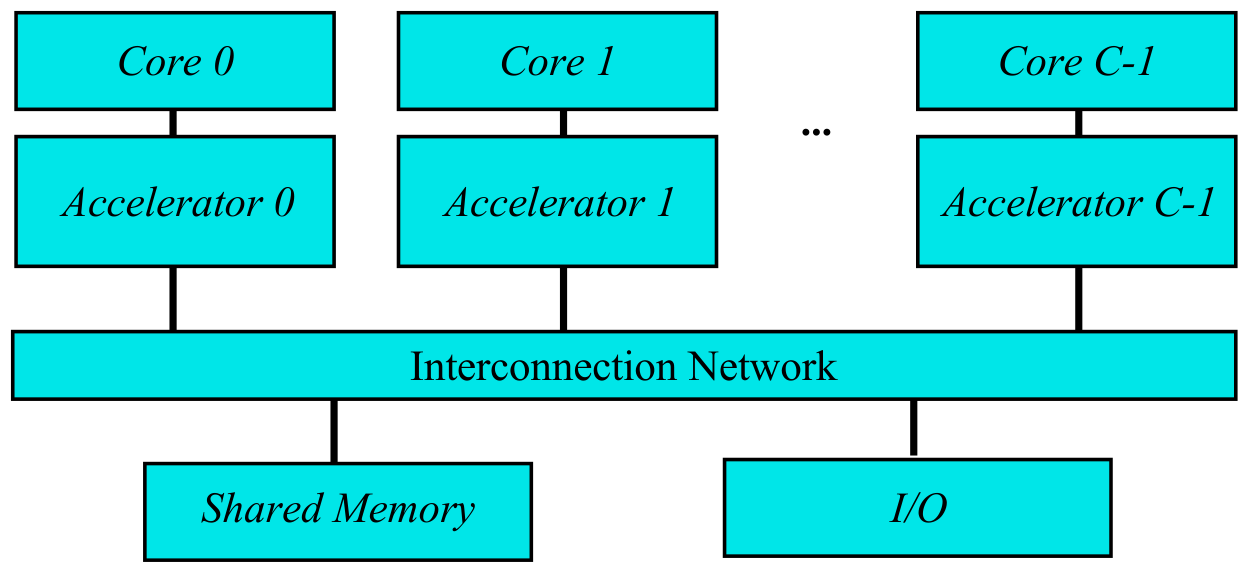
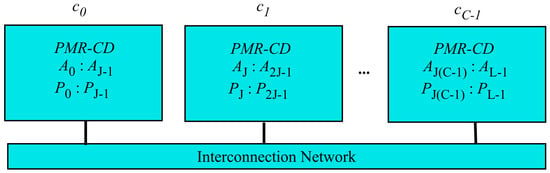
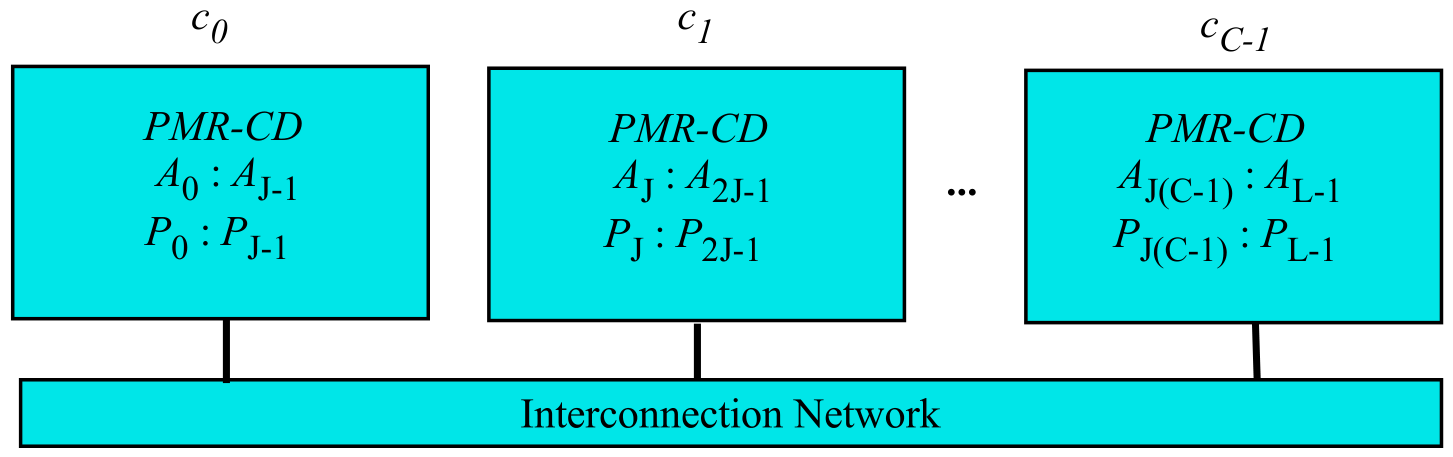
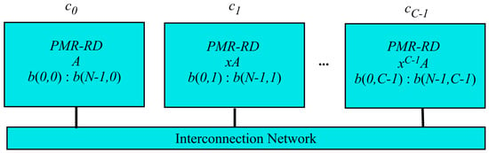
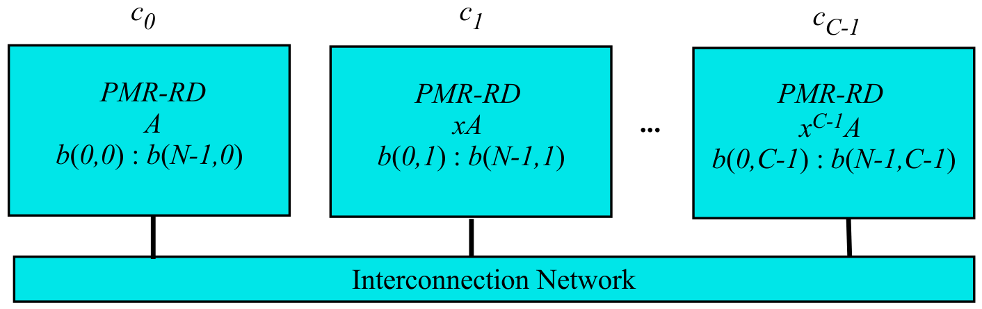
The PMR algorithm in Section 3 is inherently bit-serial in nature. The iterations to calculate the partial product shift the multiplier by the factor in Equation (16). Our aim is to partition the multiplication operation among C accelerators in the embedded multicore system shown in Figure 3.
Figure 3.
Multicore system for parallel implementation of the PMR modular multiplication algorithm.
First, we should note that iteration i of the simple PMR algorithm in Equation (16) determines when the iteration is performed on the accelerator. The multiple accelerator system requires determining three tasks associated with each iteration value i:
- 1.
- How to divide the modular multiplication among the cores;
- 2.
- When to do the different iterations;
- 3.
- Which accelerator core is assigned to do iteration i.
We propose two multicore design options, as explained in the following two sections.
5. Multicore PMR with Column Division (PMR-CD)
Our primary architecture achieves spatial concurrency by segmenting the L multiplier words across the multicore grid. The resulting allocation factor J, representing the number of words mapped to each core, is defined by
The upper bound on the number of scalable cores in this architecture is governed by L, the number of words per row.
The mapping criteria that binds a specific multiplier word to its designated processing core c is established by the following expression:
The mapping scheme for allocating the multiplier words and the corresponding partial product components across the processing grid is demonstrated in Table 2. This example is configured for an architectural environment where , , , , and .
Table 2.
Assigned multiplier and partial product words and . Case when , , , , and .
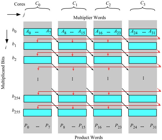
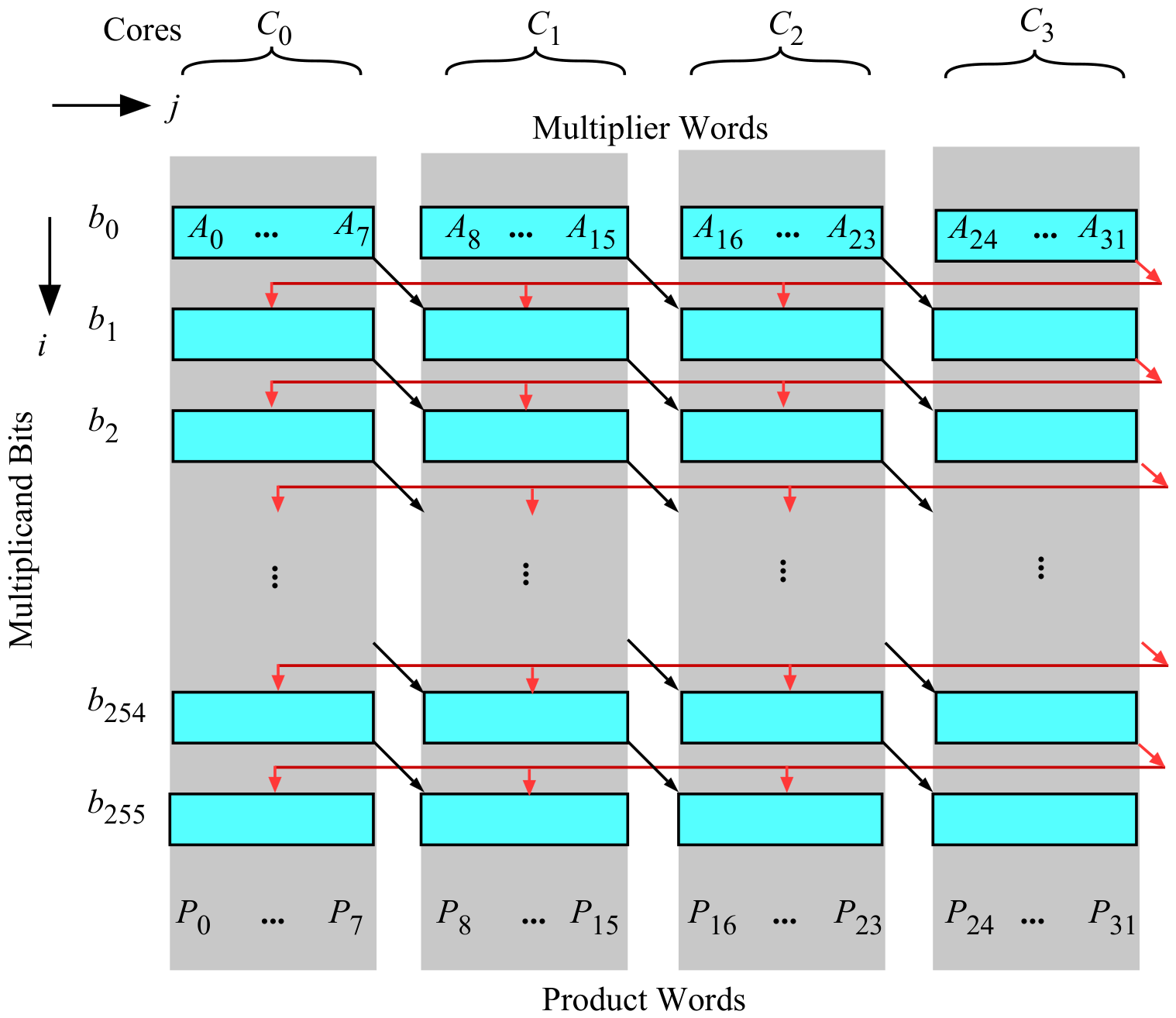
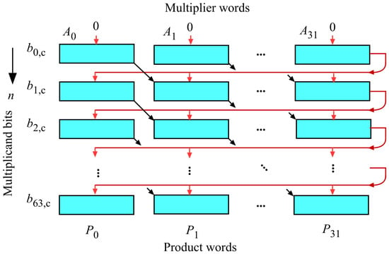
To summarize the proposed design of the PMR-CD architecture, each processing core is allocated J contiguous multiplier words. Each core is responsible for processing the m rows associated with its designated block. Figure 4 illustrates the distribution of columns and rows for each core in the scenario where , , , , and . The red arrows show the coefficients of . Some of those are zero, depending on which is chosen.
Figure 4.
Multicore PMR algorithm with column division (PMR-CD). Column-wise workload distribution across the multicore processing array for an architectural configuration defined by , , , , and . The red arrows show the coefficients of . Some of those are zero, depending on which is chosen.
The allocation of multiplier words to the processing cores necessitates data exchange between them, as indicated by the black and red arrows. This intercore communication is facilitated through the interconnection network depicted in Figure 3.
Our strategy for the PMR-CD algorithm involves applying Equation (33) to distribute the multiplier and partial product words among the cores. Consequently, the iterations in Equations (16)–(18) can be modified within our proposed approach as follows:
where means concatenate word A and word B.
The progressive multiplier reduction flow begins with Equation (34), which initializes the iterations for each core. Subsequently, Equations (35) and (36) execute the core-specific processing phases, before Equation (37) terminates the process to collect the final reduced product. Crucially, the operations defined across Equations (34)–(37) are executed concurrently by all processing cores.
The proposed PMR-CD architecture is specifically engineered to optimize intercore communication and eliminate interconnection overhead. As illustrated in Figure 4, data exchanges during execution are strictly confined to direct, point-to-point neighbor-to-neighbor links and a single broadcast line. In each iteration, the rightmost processing element transmits the reduction terms of the shifted polynomial from the preceding cycle across the shared bus. Because this broadcast originates from a single dedicated source per iteration, the network remains completely free of bus access conflicts and arbitration contention, requiring no multi-master routing or buffering hardware. Furthermore, upon algorithm completion, each core natively yields its portion of the final result, entirely bypassing the need for a final data aggregation phase or post-processing communication. Consequently, the intercore communication network operates with negligible silicon area impact and zero execution delay overhead.
6. Multicore PMR with Row Division (PMR-RD)
The second architectural scheme introduced herein processes the variables localized at iteration i and column j. Within this framework, three distinct categories of data are managed: the intermediate multiplier components , the evolving partial product vectors , and the individual multiplicand bits . The underlying data is segmented into N distinct blocks, whereby each respective block is assigned to a designated processing core according to the relation
To guarantee that the field dimension m is a strict integer multiple of the core count C, the most significant bit positions of m can be padded with zero values. The data words situated at row i are subsequently allocated to a designated core based on the following mapping criteria:
In the above equation, the quotient n and remainder c have the bounds
where N is given by Equation (38).
Multiplicand bit in row i is now double-indexed with n and c:
where the indices i, n, and c are interconnected via Equation (39). The notation specifies that the multiplicand bit is mapped to core c for execution during iteration step n. To clarify this distribution, Table 3 demonstrates the spatial allocation of multiplicand bits across the available core grid for a specific scenario where , , and .
Table 3.
Multiplicand bit distribution across the processing cores within the PMR-RD architecture, illustrated for a parameter configuration of , , and .
Our strategy for the PMR-RD algorithm involves replacing the iteration index i with the quotient n and the remainder c. This approach stems from analyzing the shifted multiplier at iteration i as presented in Equation (14). Utilizing Equation (39), we can express
The iterations defined in Equations (15)–(18) can now be modified within our proposed technique as follows:
It is worth emphasizing that the initialization tasks defined in Equation (43) comprise C independent components that lend themselves to concurrent execution. Within this execution phase, each accelerator core c evaluates its corresponding initialization variables, and . Thus, the residual value c directly identifies the specific processing node responsible for the calculation. Furthermore, the quotient index n obtained from Equation (39) is applied to track the iterative progression n within Equations (44) and (45). Adopting this structural notation, Figure 5 maps out the algorithmic dependence graph for the parallel PMR-RD framework under the conditions , , , , and . The red arrows show the coefficients of . Some of those are zero, depending on which is chosen.
Figure 5.
Multicore PMR-RD algorithm dependence graph (DG) for the iterations in core c. Case when , , , and . The red arrows show the coefficients of . Some of those are zero, depending on which is chosen.
As illustrated in the diagram, every word undergoes a leftward shift by a factor of bit positions into the adjacent higher-order word location before advancing to the subsequent row. The highest-order word within each row corresponds to the polynomial derived from Lemma 2 and is visually highlighted using red-bordered rectangles. This shifting operation, equivalent to a multiplication by , is designated by the red arrows positioned on the right margin of each respective row.
It is noteworthy that deploying a core architecture decreases the row-processing requirement for each individual core from down to . Scaling up the core count yields a proportional reduction in the computational workload per processing element, offering a distinct advantage over the systolic PMR algorithm implementations detailed in [23].
The proposed PMR-RD multicore design is specifically structured to eliminate intercore communication overhead during active iterative execution. By allowing each processing element to maintain and update its intermediate data locally within dedicated registers, the architecture completely avoids intercore bus traffic throughout the main execution phase. Upon completion of all iteration cycles, a single designated core sequentially collects and accumulates the partial results distributed across the remaining cores. Because this final accumulation phase proceeds in a deterministic, turn-based sequence using simple point-to-point transfers, the communication path remains entirely free of bus access conflicts, arbitration delays, or complex interconnect logic. Consequently, the intercore communication network introduces negligible physical resource consumption and zero routing overhead to the system architecture.
6.1. Proposed PMR-RD: Algorithm Stages
We conduct the multicore modular multiplication technique in three distinct stages:
- 1.
- Initialization stage (could be parallelized using accelerator cores);
- 2.
- Iterations stage (could be parallelized using accelerator cores);
- 3.
- Termination stage (inherently sequential).
6.1.1. PMR-RD Initialization Stage
In order to eliminate communication between the cores, the pre-processing or initialization stage ensures that the different shifted versions of are evaluated at each accelerator core and prepared as follows:
- 1.
- The multiplier A is broadcast by the I/O to all of the accelerator cores;
- 2.
- Accelerator core c calculates the initial shifted multiplier and initial partial product
where the index c in this notation refers to the c-th accelerator core.
Algorithm 1 outlines the steps involved during the initialization phase. Essentially, there are two variables that need to be initialized: the shifted multiplier and the partial product P.
| Algorithm 1 Initialization stage of the proposed multicore multiplication algorithm |
|
6.1.2. PMR-RD Iteration Stage
The iteration stage replaces the single operations in Equations (16) and (17) with c operations for both variables. All cores operate simultaneously, such that each core performs the single operations specified in Equations (16) and (17). More importantly, the shift value now replaces x.
Fundamentally, the procedure partitions the m computational rows from Table 1 into C distinct segments, where each individual block encompasses rows. To guarantee that the total row count m is perfectly divisible by the available core count C, supplementary rows are appended at the lower boundary, accompanied by zero-padding at the most significant bit (MSB) positions of the multiplicand operand B. The operational flow of this iterative phase for the proposed multicore PMR multiplier accelerator is formalized in Algorithm 2.
| Algorithm 2 PMR-RD iteration stage. |
|
As specified in Line 3 of Algorithm 2, the reduction procedure leverages the C higher-order bits of the multiplier component . The concurrent execution framework, spanning Lines 1 through 6 of Algorithm 2, is managed via a PARALLEL FOR construct where each independent execution branch is mapped to one of the C available hardware accelerator cores.
6.1.3. PMR-RD Termination Stage
The termination stage is entirely sequential and is responsible for producing the required modular product P. One of the accelerator cores is designated to compute the final product, and this core contacts all of the other cores to retrieve their copies of the partial product . Consequently, the generation of the final output product is conducted as follows:
Algorithm 3 summarizes these operations.
| Algorithm 3 PMR-RD algorithm termination stage |
|
7. Implementations of Modular Multiplication Algorithms
The subsequent subsections evaluate four primary structural configurations designed for executing modular multiplication over . Specifically, Section 7.1 explores the multiply-then-reduce (MtR) approach, followed by an analysis of the standard progressive multiplier reduction (PMR) technique in Section 7.2. We then investigate two multicore variants incorporating row division, denoted as PMR-CD and PMR-RD, in Section 7.3 and Section 7.4, respectively. Each hardware implementation reviewed in this study assumes an underlying processor architecture tailored to support the respective algorithmic flow.
7.1. MtR Implementation
The multiply-then-reduce strategy executes polynomial multiplication using two m-term polynomials, A and B, yielding an intermediate product polynomial P comprising terms. It is not practical to use a parallel multiplier to do the multiplication, due to area limitations. The reason why the parallel multiplier accepts only half-words is to produce a full-word product. Since all algorithms will be implemented on the same multicore embedded system, the clock period of the cores will be chosen to be larger than the largest delay of any of the four algorithms enumerated above. The estimates of delays are derived in Section 8.
Assume that the processor to perform modular multiplication has word size W bits. It is natural therefore to express the polynomials A and B in terms of words:
where the number of words is L as given in Equation (25).
It is not practical to design an multiplier, due to several reasons:
- 1.
- It is not practical to move m-bit words on the processor bus, especially when m varies with the field in use.
- 2.
- It is not practical to implement an parallel multiplier, particularly when m varies with the field in use.
- 3.
- It is not practical to design m-bit registers, especially when m varies with the field in use.
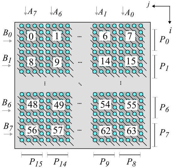
A better approach is to design a partitioned multiplier. Figure 6 shows how an polynomial multiplier is partitioned using smaller multipliers for the case when , , and . The general direction for the flow of data among the blocks is from top to bottom and from left to right.
Figure 6.
Partitioning an polynomial multiplier using smaller multipliers. Case , , and .
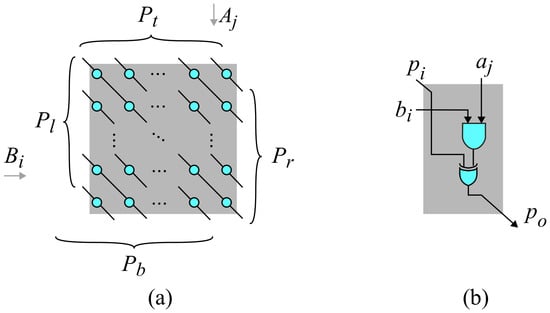
The multiplier is shown in more detail in Figure 7.
Figure 7.
Detail of the multiplier. (a) Inputs and outputs of the multiplier. (b) Detail of a single cell (blue circle).
Figure 7a shows the inputs and outputs of the multiplier. The multiplier accepts the following inputs:
- 1.
- Input word from the top ();
- 2.
- Input word from the left ().
Similarly, the partitioned multiplier produces the following outputs:
- 1.
- Output word from the bottom ();
- 2.
- Output word from the right ().
Figure 7b shows details of a single cell (blue circle).
The product has bits or words, as shown at the right and bottom edges of Figure 6. The numbers inside each block represent the time of executing the block. Each cell is composed of an AND gate to generate the product bit , and the resulting partial product is given by
The scheduling of the functional blocks is designed to ensure that precisely one multiplier word and one multiplicand word are delivered to a given block at any specific time step. Consequently, the temporal execution assigned to the multiplier unit situated at row i and column j in Figure 6 is defined by the following scheduling function:
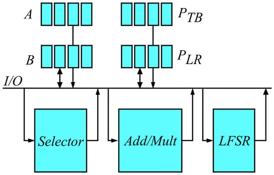
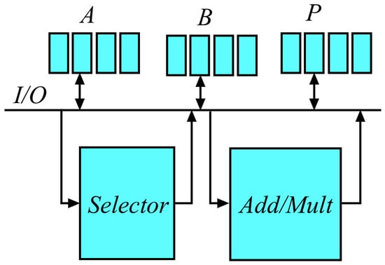
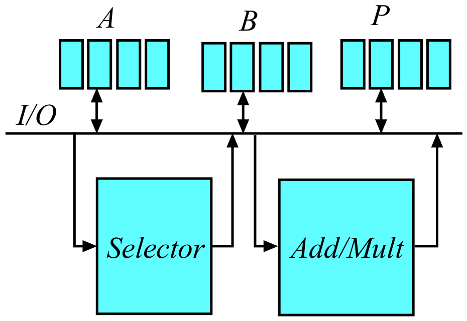
Figure 8 shows the processor that performs the MtR algorithm. The processor’s multiplier/adder is composed of three main modules: The first module is the selector that accepts an input W-bit word and produces two outputs, as will be discussed below. The second module is the multiply–add that performs multiplication as well as performing the addition operation. The third module is the linear feedback shift register (LFSR) that performs polynomial reduction.
Figure 8.
Structural layout of the MtR processor.
As illustrated in Figure 8, the internal architecture of the MtR processor incorporates four distinct register banks:
- 1.
- At the top-left corner of the figure are two W-bit register banks, with L registers each, to store the multiplier A and multiplicand B.
- 2.
- At the top-right corner of the figure are two W-bit register banks and , with L registers each, to store the intermediate product results and the final product.
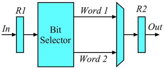
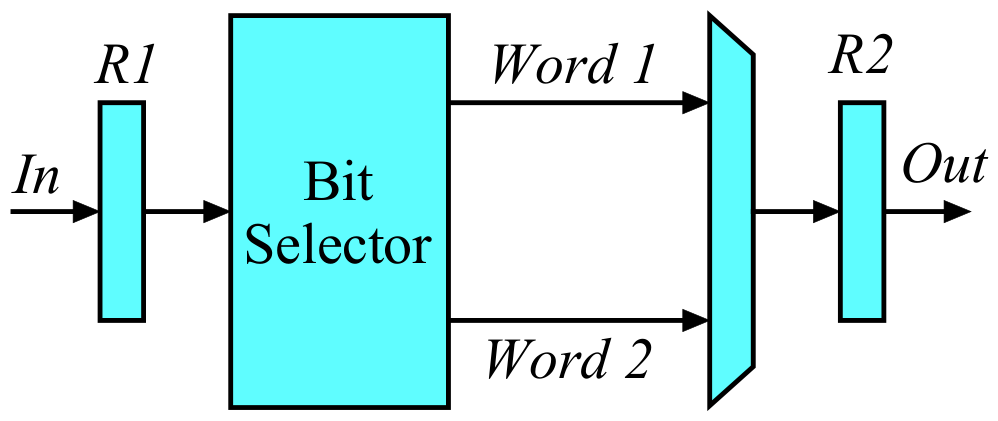
There is specialized hardware to do data shifting and do final product reduction using the LFSR. Figure 9 shows the detail of the selector block in Figure 8.
Figure 9.
The bit selector structure.
The selector accepts one word at its input and the bit selector produces two output words Word 1 and Word 2. These two output words are selected according to the following expressions:
Figure 10.
Structure of the MtR multiplier/adder.
The MtR multiplier/adder has two components: the multiplier, whose structure is shown in Figure 7; and the W-bit adder, which is composed of W two-input XOR gates.
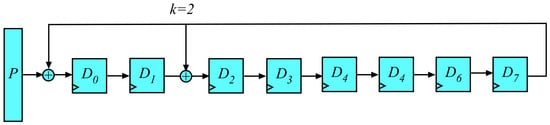
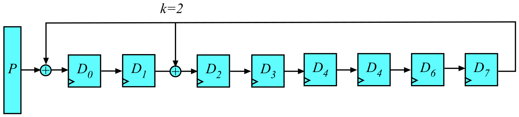
Figure 11 performs the reduction of the -bit product P using a linear feedback shift register (LFSR). The figure shows a Galois LFSR for the case when the primitive polynomial is , and this is indicated by the two feedback inputs feeding the inputs of flip-flops and . The LFSR accepts bit-serial data, and this is accomplished using a parallel-to-serial register converter, as shown on the left of the figure.
Figure 11.
Galois LFSR commonly used for reducing an input polynomial P. Case when the primitive polynomial is .
7.2. Implementation of Standard PMR Algorithm
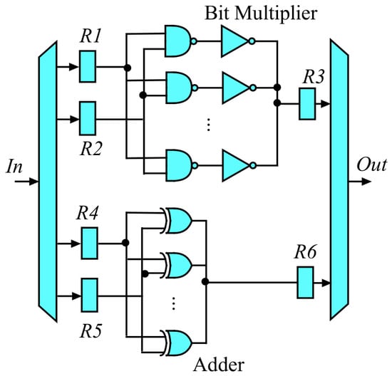
Figure 12 shows the processor that performs the PMR algorithm, as was explained in Table 1 and the corresponding iterations in Equations (28)–(31).
Figure 12.
Processor structure for the word-based PMR algorithm.
The details of the PMR selector are shown in Figure 9. Figure 13 shows the detail of the PMR multiply/add module.
Figure 13.
Details of the PMR multiplier/adder.
The PMR processor maintains three register banks, as follows:
- 1.
- Two W-bit register banks, with L registers each, to store the multiplier A and multiplicand B;
- 2.
- One W-bit register bank P, with L registers, to store the partial product results and the final product.
The operational orchestration of word processing across the hardware blocks is governed by a precise time-scheduling function. For a multiplier word located at spatial row coordinates i and column coordinates j, the specific execution time slot is systematically allocated using the following linear scheduling relationship:
This scheduling function coordinates the sequential routing of operands from the register banks over successive clock cycles, matching the programmatic algorithm iterations.
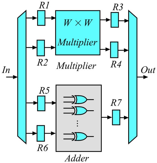
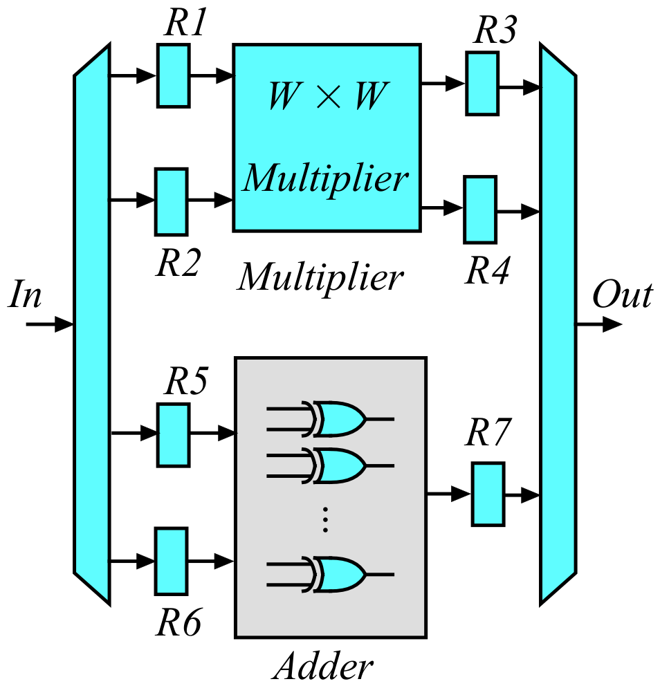
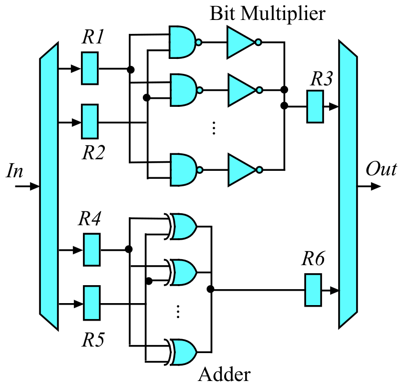
The mathematical operations are partitioned between two specialized processing units connected to the I/O bus: a PMR selector that interfaces directly with the A and B register files to prepare operand sub-words, and an Add/Mult module that executes calculations through dual logical pathways. As shown in the gate-level diagram of Figure 12, the module’s bit multiplier path passes de-multiplexed operands into registers and to perform word-based bitwise multiplication using parallel NAND gates and bit-inverters, capturing the results in register . Simultaneously, the adder path routes operands via registers and to a parallel array of XOR-based adders for finite-field additions, buffering the sum in register before updating the partial product bank P over the system bus.
7.3. Implementation of PMR-CD Option
The spatial partitioning of the multiplier words across the multicore framework is illustrated in Figure 4. Building upon this distribution, Figure 14 presents the complete multicore hardware architecture implementing the parallel PMR-CD algorithm.
Figure 14.
Implementation of the PMR-CD algorithm. Each core operates on J columns of the multiplier words and all of the multiplicand bits.
The internal organization of each core follows the architecture illustrated in Figure 12; however, execution within an individual core is restricted to J multiplier words alongside the complete set of multiplicand bits. Specifically, core c manipulates J consecutive words of both the multiplier and the partial product, while simultaneously utilizing all available multiplicand bits.
To implement the PMR-CD algorithm on a multicore system, we need to do two operations: (i) projecting the words shown in Figure 4 to the processor or each core, and (ii) scheduling the workload of each core shown in Table 4.
Table 4.
Iteration scheduling for the multicore implementation of the PMR-CD algorithms. Case , , , , and .
7.3.1. Projection Function Design for PMR-CD
Equation (33) defines the selected projection function, which maps each distinct partial product or multiplier word, or , within the column limits to a designated processing core.
7.3.2. Scheduling Function Design for PMR-CD
The projection function specified by Equation (33) dictates our choice of the timing function. We have some considerations that must be observed:
- 1.
- All cores processing the L words in a given row operate in parallel;
- 2.
The specific time coordinate mapped to the evaluation of the multiplier and partial product words and during the i-th iteration at column position j is formulated as follows:
Table 4 presents the step-by-step iteration timing metrics governing the parallel PMR-CD accelerator design, constrained to the first J column segments under the operational conditions , , , , and .
7.4. Implementation of PMR-RD Option
Figure 5 shows how the multiplicand bits are assigned to the cores. Each core operates on N multiplicand bits. Figure 15 illustrates the multicore implementation of the PMR-RD algorithm, where core c uses the following:
Figure 15.
Hardware implementation of the PMR-RD architecture, where each individual core executes operations across the entire set of multiplier words using a localized subset of N multiplicand bits.
The PMR-RD dependence graph in Figure 5 is merely a graph showing how the algorithm variables depend on the algorithm indices. It does not give any indication on the scheduling of the operations or on which processing element is assigned to the algorithm tasks. Specifically, scheduling function determines the execution time associated with each node (scheduling function), and the projection function determines which processing element (PE) or software thread is assigned to a node.
The authors of [24] proposed specialized accelerators designed to efficiently implement the PMR algorithm. The main motivations were to control the processor workload and optimize the latency of the algorithm. The primary objective of this study is to map the PMR algorithm onto an embedded multicore platform composed of C processing cores. This architectural deployment directly influences the underlying scheduling and spatial projection functions, as detailed in the subsequent sections. We prioritize the formulation of the projection function first, as it establishes the framework for embedding the algorithm into the multicore system.
7.4.1. Projection Function Design for PMR-RD
Let and represent the multiplier and partial product words, respectively, at iteration index i and column index j, defined over the domains and . These data words are allocated to a specific core c based on the spatial mapping criteria detailed in Equation (39). To illustrate this distribution framework within an embedded multicore environment, Table 5 outlines the exact allocation of multiplier words to processing units for an architectural instance where and .
Table 5.
Allocation framework of multiplier words across the processing cores for an architectural configuration where and .
Under this allocation paradigm, the multiplier and partial product words are divided among the available processing elements such that each core manages an N-word subset determined by Equation (38). As indicated by the table, core handles an eight-word slice of the multiplier array, specifically tracking the elements .
7.4.2. Scheduling Function Design for PMR-RD
The dependence graph is mapped into a directed acyclic graph () via the scheduling function. Utilizing a formal design methodology, the authors of [24] derived all feasible and practical scheduling formulations for the PMR algorithm. Among the two identified functions, one specifically enables the system designer to regulate both the quantity of systolic processing elements and the individual processor workload. Equation (39) governs the assignment of multiplier and partial product words to specific cores alongside the execution timeline for the update expressions at each iteration step. This underlying function satisfies two main criteria: every core must compute all of the words within a designated row, and all cores must operate simultaneously on distinct rows. Consequently, the multiplier and product words, and , are bound by the temporal scheduling function
where the scaling factor of 2 accounts for the requirement to update both and during every iterative cycle.
8. Complexity Analysis of the Modular Multiplication Algorithms
In this section, we compare the delay, area, and area–delay product to complete the modular multiplication implementations. We start this section with a brief overview of power consumption source in a CMOS integrated circuit. We try to relate this power consumption to the chip area and argue that area × delay product (ADP) is equivalent to the energy consumption of the chip.
8.1. Sources of Power Consumption
Total power dissipation is fundamentally composed of static leakage, dynamic switching, and short-circuit overlap current during logic transitions. Because static leakage is governed by the source and drain diffusion regions that form the semiconductor junctions, it can be closely approximated as being proportional to the total gate area. The dynamic component of power consumption is formally defined by the relation
where C denotes the parasitic capacitance, f represents the operating frequency, and is the supply voltage. Assuming uniform values for both f and , the dynamic dissipation scales primarily with the parasitic capacitance. Given that this capacitance is directly tied to the transistor’s physical source and drain dimensions, dynamic power also exhibits a linear proportionality to the gate area.
Conversely, overlap power dissipation occurs during the finite transition window when a logic gate is switching between states and passes through an intermediate voltage level. Within this transient phase, the current flow scales with the gate’s driving strength, which is a function of channel width rather than total area. Consequently, overlap current is the sole power component independent of gate area. Because automated CAD synthesis tools and circuit designers aggressively minimize short-circuit overlap to prevent performance degradation, this component is omitted from our high-level analysis. We therefore focus exclusively on static leakage and dynamic switching as the predominant power contributors, treating total power as proportional to the aggregate gate area. Furthermore, because all four modular multiplication architectures utilize identical core designs, the total energy consumption scales directly with the execution delay required to complete each respective algorithm.
8.2. Normalizing Gate Delay and Area Based on Basic Inverter Gate
When a system operates, all gates and components have the same f and values. The power performance becomes determined mainly by the parasitic capacitances C. The value of the capacitance C also depends on the transistor area. Therefore, we can argue that estimates of area are also proportional to power.
The delay and area performance metrics for the foundational gates and circuits utilized in finite-field arithmetic architectures are summarized in Table 6. To establish a standardized baseline, the physical area is normalized relative to a minimum-area nMOS transistor, while the propagation delay is normalized against a minimum-area inverter. The implementation of the edge-triggered D-type flip-flop is based on the NAND-gate configuration detailed in [25]. Furthermore, all structural optimization choices aimed at achieving minimum gate delay conform to established VLSI design methodologies, such as those presented in [26].
Table 6.
Normalized delay and area of major components used in field arithmetic hardware.
Evaluating the propagation delay of the proposed hardware architectures requires a precise estimation of the clock cycle count consumed by each computational phase of the modular multiplication algorithms. To facilitate this analysis, a set of foundational register-transfer level (RTL) instructions is formalized for the various hardware configurations under study. These core RTL operations are summarized in Table 7.
Table 7.
Basic RTL instructions for the processors used to effect the modular multiplication algorithms.
To demonstrate the practical application of the RTL, Figure 16 illustrates the execution of a multiplication operation within the multiplier architecture of Figure 10. In this setup, the multiplication block generates two distinct W-bit outputs consisting of the least significant word (LSW) and the most significant word (MSW). As detailed in the execution diagram, the complete multiplication routine requires exactly five clock cycles to compute the final results.
Figure 16.
RTL code for loading and multiplying two values stored in registers and and storing the two LSW products in register and MSW product in .
8.3. Complexity Analysis of the MtR Algorithm
As illustrated in Figure 8, the operational clock period is bounded by the cumulative propagation delay of three critical modules:
Examination of Figure 9, Figure 10 and Figure 11 reveals that the maximum delay of the modules is governed by . Therefore, we can write
The total clock cycle count required to execute the MtR algorithm is determined by analyzing its machine-level instruction trace, assuming a single-cycle execution model for each discrete operation. This algorithmic evaluation establishes the following total cycle formulation:
The total delay of the MtR algorithm is therefore given by
With reference to Figure 8, the area of the MtR processor is estimated as
where is the area of the registers (Figure 8), is the area of the selector (Figure 9), is the area of the multiplier (Figure 7), is the area of the adder (Figure 10), and is the areas of the linear feedback shift register (Figure 11). We can write these areas as follows:
The area–delay product estimate to perform the MtR algorithm is given by
8.4. Complexity Analysis of the PMR Algorithm
As illustrated in Figure 12, the operational clock period is bounded by the cumulative propagation delay through two primary modules:
Examination of Figure 9 and Figure 13 reveals that the maximum delay of the modules is governed by . Therefore, we can write
The total clock cycle count required to execute the PMR algorithm is derived by tracking its machine-level instruction trace under a single-cycle execution model. This structural analysis provides the following mathematical expression for the total cycles:
Based on these timing metrics, the cumulative delay profile for the PMR algorithm is determined by
Based on the architectural layout presented in Figure 12, the total hardware area footprint of the PMR processor is approximated by
where we have
The area–delay product estimate to perform the PMR algorithm is given by
8.5. Complexity Analysis of the PMR-CD Algorithm
The hardware operating clock period is dictated by Equation (71). To calculate the cumulative cycle count of the PMR-CD architecture, we trace the underlying machine-level micro-operations under a uniform single-cycle execution model, which establishes the following mathematical expression for the total cycles:
Consequently, the aggregate execution delay of the PMR-CD algorithm is formulated as follows:
Utilizing the component breakdown illustrated in Figure 12, the structural area complexity of the PMR-CD execution unit is formalized by
where we have
The area–delay product estimate to perform the PMR-CD algorithm is given by
8.6. Complexity Analysis of the PMR-RD Algorithm
The operating clock period is given by Equation (71). To determine the overall cycle count for the PMR-RD algorithm, we monitor the machine-level instruction trace under a uniform single-cycle execution model, which establishes the following expression for the total cycles:
Based on these timing metrics, the cumulative delay profile for the PMR-RD scheme is determined by
Based on the architectural layout presented in Figure 12, the total hardware area footprint of the PMR-RD processor is approximated by
where we have
The area–delay product estimate to perform the PMR-RD algorithm is given by
9. Results and Discussion
In this section, we present a comprehensive performance evaluation and comparative analysis of the proposed progressive multiplier reduction (PMR) architectures. To demonstrate scalability and hardware efficiency, we compare the PMR-CD and PMR-RD variants against baseline MtR and conventional PMR designs over the parameter range , with and core counts . This evaluation focuses specifically on three key metrics: normalized hardware area, normalized execution latency, and normalized area–delay product (ADP)/energy overhead.
9.1. Performance of PMR-CD Algorithms
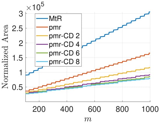
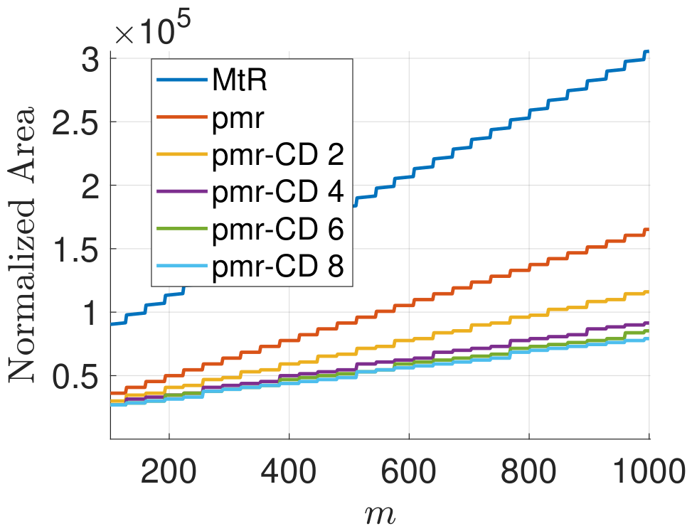
The normalized hardware area overhead for the MtR, PMR, and PMR-CD configurations is illustrated in Figure 17, evaluated across the key parameter spaces , a word size of , and core counts . The results indicate that the baseline MtR architecture consumes the largest area footprint among all evaluated schemes. Conversely, both multicore PMR strategies yield a substantial reduction in silicon area compared to the traditional implementations, highlighting the physical resource efficiency inherent to the decentralized multicore topology.
Figure 17.
Normalized area comparison for MtR, PMR, and PMR-CD algorithms (, , ).
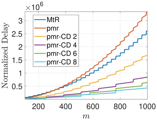
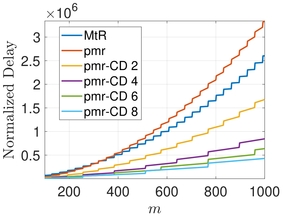
The execution delay profiles for the MtR, PMR, and PMR-CD configurations are plotted in Figure 18, evaluating performance over the range with a word width of across core counts . Among the evaluated architectures, the standard PMR system exhibits the maximum processing latency. Conversely, the PMR-CD variants display distinct step-like latency variations, which stem directly from the discrete boundary parameters J and L formulated in Equations (25) and (32). The lower bounds of the plot correspond to the multicore implementations, which deliver the most substantial latency savings. This optimization is driven by allocating multiplier segments and partial product blocks across parallel processing elements. Although expanding the core count yields shorter delays, this performance advantage starts to saturate beyond eight cores, indicating a practical scaling threshold under current operational constraints. This trend of diminishing returns is analytically explained by the inverse dependence on C in Equation (32), where the derivative () bounds the marginal latency reduction per additional core. Furthermore, because the architecture employs dedicated point-to-point and broadcast links, this saturation is strictly governed by workload division limits rather than interconnect network bottlenecks or routing contention.
Figure 18.
Normalized delay comparison for MtR, PMR, and PMR-CD algorithms (, , ).
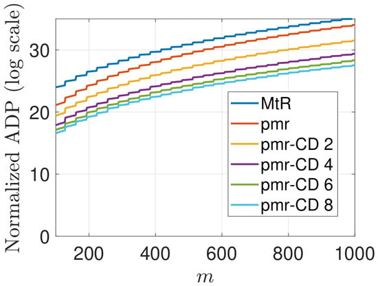
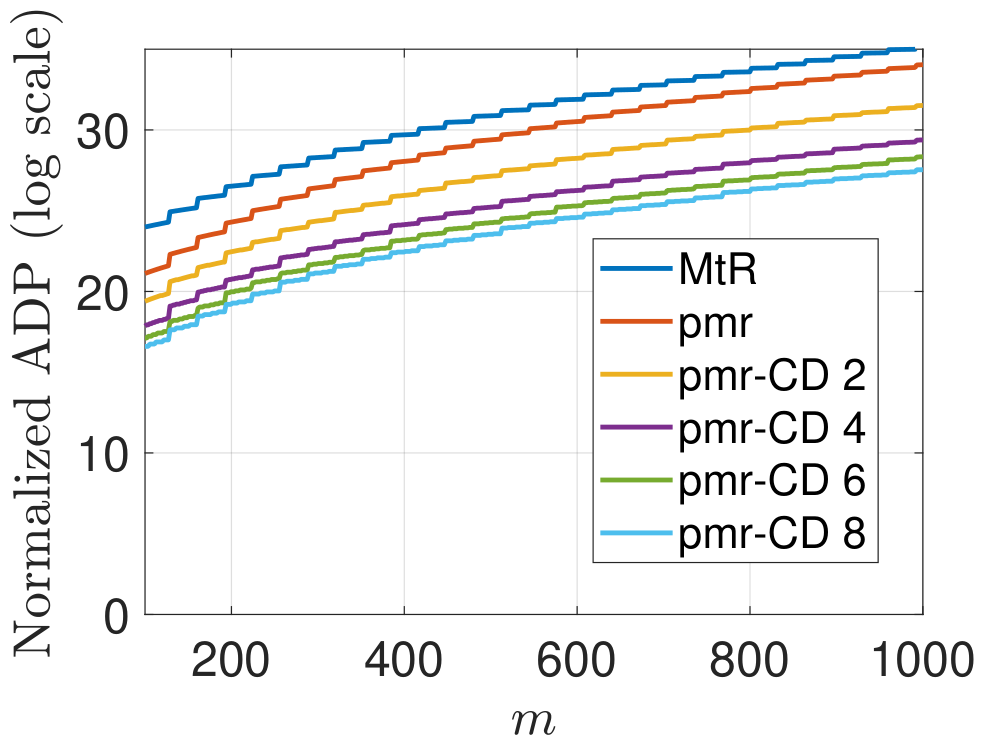
The normalized ADP/energy profiles for the MtR, PMR, and PMR-CD configurations are illustrated in Figure 19, assuming a parameter space of , a word size of , and core scaling factors . The curves indicate that the baseline MtR framework incurs the maximum ADP, marking it as the most resource-intensive design under evaluation. Conversely, the PMR-CD strategy yields a substantial enhancement in hardware efficiency, where ADP metrics scale down monotonically with the integration of additional processing cores. Given that power dissipation scales with total silicon area, the normalized ADP provides a dependable metric for evaluating relative energy overhead. These findings thus verify that the system energy consumption diminishes as a direct function of core expansion. This characteristic emphasizes the efficiency advantages of the multicore PMR-CD topology, which effectively minimizes the operational energy footprint by simultaneously accelerating execution paths and compacting physical resource usage.
Figure 19.
Normalized ADP/energy comparison for MtR, PMR, and PMR-CD algorithms (, , ).
9.2. Performance of PMR-RD Algorithms
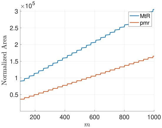
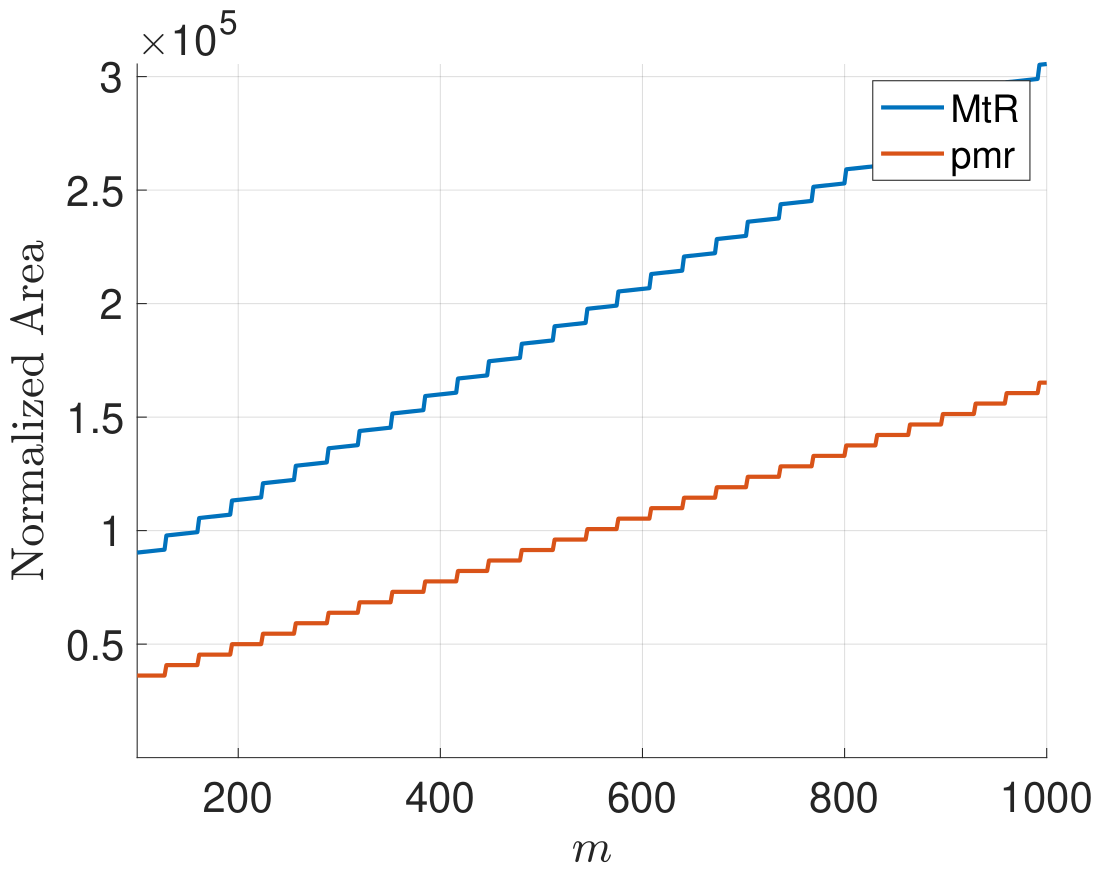
The normalized hardware area overhead for the MtR, PMR, and PMR-RD implementations is illustrated in Figure 20, evaluated across the parameter space , a word size of , and core counts . A prominent finding is that the normalized area for every PMR-derived variant remains completely static across all core variations, as evidenced by the coincident red plotline. This behavior indicates that the physical resource footprint of the PMR-RD architecture is invariant to changes in the degree of hardware parallelism. As expected, the traditional MtR framework consumes the largest silicon area among all considered configurations. Although the PMR-RD variants secure a substantial area reduction over the baseline MtR design, they lack the multicore area-scaling dynamics characteristic of alternative topologies. This outcome underlines that while PMR-RD provides superior area efficiency relative to MtR, its architectural benefits are optimized for performance indices outside of physical area minimization during core scaling.
Figure 20.
Normalized area comparison for MtR, PMR, and PMR-RD algorithms (, , ).
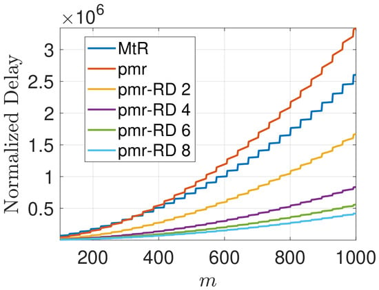
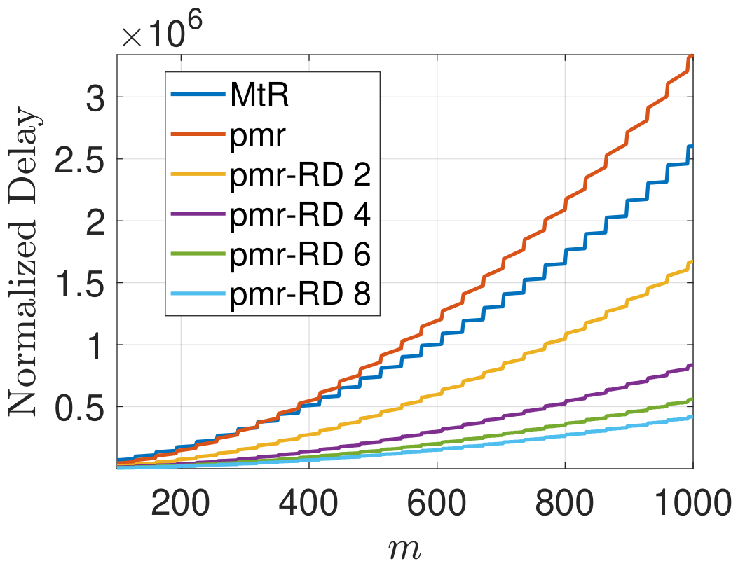
The execution delay metrics for the MtR, PMR, and PMR-RD architectures are plotted in Figure 21, evaluated across a parameter sweep of , a word size of , and parallel core scales . Analogous to the CD variant, the PMR-RD framework displays distinct step-like latency variations dictated by the discrete parameters J and L from Equations (25) and (38). Among the analyzed systems, the conventional PMR scheme exhibits the highest processing latency, outperforming neither the MtR nor the parallelized PMR options. The lower bounds of the plot correspond to the multicore PMR-RD implementations, which yield the most substantial speedups. By partitioning and mapping specific word segments of the multiplier or partial products across concurrent cores, the design successfully accelerates the workload as C expands. Nonetheless, this latency optimization follows a trend of diminishing returns, where scaling past the eight-core threshold produces increasingly marginal performance gains. This behavior is theoretically governed by the inverse dependence on C in Equation (38), whose derivative () limits per-core delay reductions as the core count scales. Moreover, this performance saturation is strictly a property of workload partitioning rather than interconnected network bottlenecks, as the dedicated point-to-point communication topology eliminates routing contention.
Figure 21.
Normalized delay comparison for MtR, PMR, and PMR-RD algorithms (, , ).
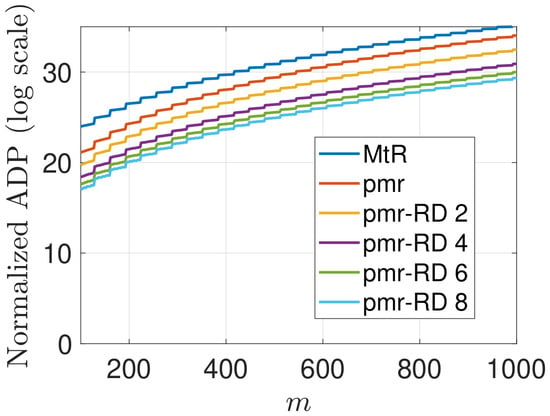
The normalized ADP/energy trends for the MtR, PMR, and PMR-RD architectures are depicted in Figure 22, assuming a parameter sweep of , a word size of , and parallel core scales . The numerical results demonstrate that the baseline MtR framework incurs the largest ADP, representing the least optimized configuration in this evaluation. In contrast, the PMR-RD strategy secures prominent gains in design efficiency, exhibiting a steady contraction in ADP as the hardware scales to higher core numbers. This behavioral profile directly influences the operational power and energy dynamics of the system. Because total power dissipation scales with the physical gate area, the normalized ADP functions as a reliable analytical estimator for relative energy expenditure. Consequently, these performance slopes verify that the system energy consumption diminishes in a nearly linear fashion as additional processing elements are integrated.
Figure 22.
Normalized ADP/energy comparison for MtR, PMR, and PMR-RD algorithms (, , ).
9.3. Performance of PMR-CD vs. PMR-RD Algorithms
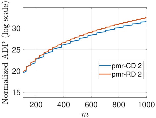
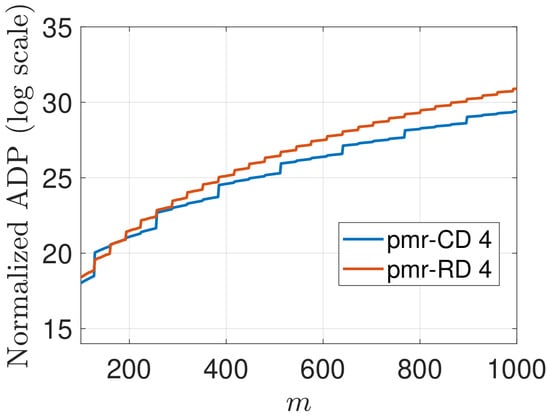
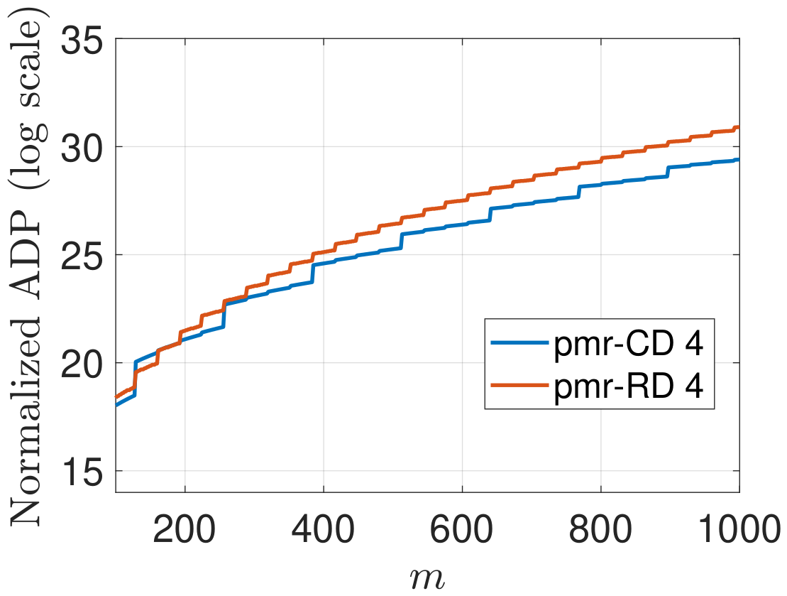
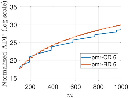
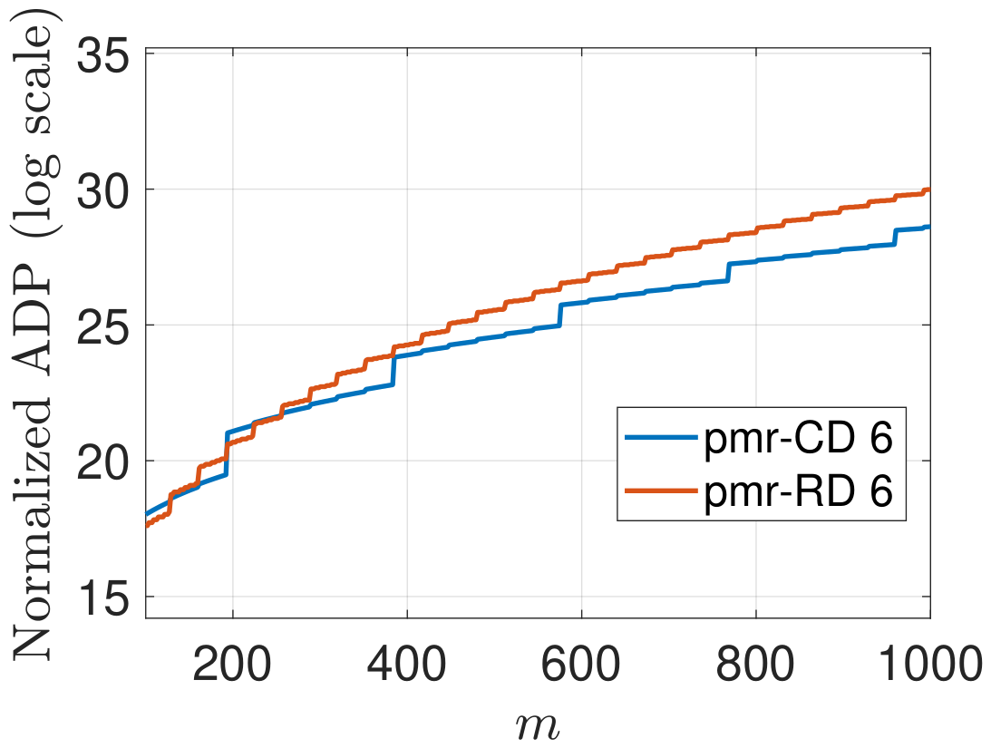
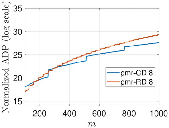
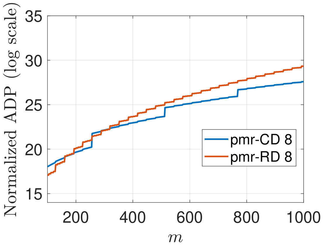
The normalized ADP and energy profiles comparing the proposed variants are plotted in Figure 23, Figure 24, Figure 25 and Figure 26, evaluating performance over the range and for parallel execution factors . Across all analyzed setups, the PMR-CD framework systematically achieves a lower ADP than the PMR-RD design, reflecting a more balanced trade-off between silicon resource allocation and execution velocity. Notably, the simulation curves demonstrate that expanding the core count monotonically reduces the aggregate ADP for both topologies, verifying that these architectures scale efficiently with enhanced hardware parallelism. This contraction in ADP maps directly to an improvement in electrical efficiency. Because dynamic power dissipation scales with total gate area, the minimized ADP of the PMR-CD topology proves its superior energy optimization relative to PMR-RD. Consequently, PMR-CD establishes itself as the more area-conscious and energy-efficient solution for multicore hardware scaling under the specified operational parameters.
Figure 23.
Normalized ADP/energy comparison between PMR-CD and PMR-RD algorithms (, , ).
Figure 24.
Normalized ADP/energy comparison between PMR-CD and PMR-RD algorithms (, , ).
Figure 25.
Normalized ADP/energy comparison between PMR-CD and PMR-RD algorithms (, , ).
Figure 26.
Normalized ADP/energy comparison between PMR-CD and PMR-RD algorithms (, , ).
10. Summary and Conclusions
This paper presents two innovative parallel mapping architectures designed to optimize finite-field modular multiplication across multicore embedded platforms: the progressive multiplier reduction with column division (PMR-CD) and progressive multiplier reduction with row division (PMR-RD) frameworks. Developed as scalable alternatives to single-core hardware setups, both topologies leverage a systematic multicore execution grid to distribute computation blocks across localized rows or columns. This targeted partitioning strategy effectively localizes intermediate data feedback within individual processing cores, minimizing cross-core communication traffic and preventing routing bottlenecks common in classic MtR pipelines. Experimental and hardware complexity metrics demonstrate that both multicore PMR designs achieve profound performance gains over standard word-based PMR and conventional multiply-then-reduce (MtR) baselines. By dividing the multiplier or partial product words across parallel core arrays, both systems yield a massive reduction in operational latency and execute with highly optimized workload distributions. Notably, the PMR-RD architecture maintains a stable, constant physical footprint during scaling, whereas the PMR-CD architecture delivers distinct area-scaling benefits and consistently demonstrates a lower ADP relative to PMR-RD across all evaluated field lengths. This minimized ADP translates into a superior energy-efficiency profile, although scaling benefits encounter diminishing returns beyond a core count of eight. Ultimately, these verified parallel execution models provide a secure, high-throughput, and energy-conscious cryptographic framework tailored for resource-constrained edge infrastructure.
Future work will focus on extending these parallel architectural frameworks from binary extension fields to prime fields . Implementing this parallel mapping in prime fields introduces two primary hardware complexities: First, inter-word carry propagation must be efficiently managed across the parallel processing cores without introducing critical path bottlenecks or timing stalls. Second, and more critically, prime-field arithmetic requires dynamic modular reduction following intermediate additions. Determining whether an intermediate sum exceeds the modulus p necessitates a hardware comparison step that typically requires an additional subtraction or addition operation. Future research will explore hardware-efficient mechanisms—such as deferred carry-save representations, redundant arithmetic formats, and speculative reduction structures—to eliminate these comparison cycles and mitigate carry-propagation overheads across parallel core grids.
Author Contributions
Conceptualization, F.G.; methodology, F.G. and A.I.; software, F.G.; validation, F.G. and A.I.; formal analysis, F.G. and A.I.; investigation, F.G. and A.I.; resources, F.G. and A.I.; data curation, F.G.; writing—original draft preparation, F.G. and A.I.; writing—review and editing, F.G. and A.I.; visualization, F.G.; supervision, F.G. and A.I.; project administration, F.G. and A.I.; funding acquisition, A.I. All authors have read and agreed to the published version of the manuscript.
Funding
This research was funded by Prince Sattam bin Abdulaziz University through project number (PSAU/2026/01/44639).
Data Availability Statement
The original contributions presented in this study are included in the article. Further inquiries can be directed to the corresponding author.
Acknowledgments
The authors extend their appreciation to Prince Sattam bin Abdulaziz University for funding this research work through the project number (PSAU/2026/01/44639).
Conflicts of Interest
The authors declare no conflicts of interest.
Abbreviations
The following abbreviations are used in this manuscript:
| ADP | Area–Delay Product |
| CMOS | Complementary Symmetry Metal–Oxide–Semiconductor |
| CPU | Central Processing Unit |
| DFF | D-Type Edge-Triggered Flip-Flop |
| DG | Dependency Graph |
| ECC | Elliptic-Curve Cryptography |
| Binary Extension Field | |
| Prime Field | |
| I/O | Input/Output |
| IoT | Internet of Things |
| LSW | Least Significant Word |
| MSB | Most Significant Bit |
| MSW | Most Significant Word |
| MtR | Multiply-then-Reduce |
| NMOS | Negative-Type Metal–Oxide–Semiconductor |
| PE | Processing Element (for systolic arrays) |
| PMOS | Positive-Type Metal–Oxide–Semiconductor |
| PMR | Progressive Multiplier Reduction |
| PMR-CD | Progressive Multiplier Reduction—Column Division |
| PMR-RD | Progressive Multiplier Reduction—Row Division |
| PUF | Physically Unclonable Function |
| RSA | Rivest–Shamir–Adleman |
References
- Islam, M.; Hossain, M.; Shahjalal, M.; Hasan, M.; Jang, Y. Area-time efficient hardware implementation of modular multiplication for elliptic curve cryptography. IEEE Access 2020, 8, 73898–73906. [Google Scholar] [CrossRef] [Scilit]
- Savaş, E.; Koç, Ç. Finite field arithmetic for cryptography. IEEE Circuits Syst. Mag. 2010, 10, 40–56. [Google Scholar] [CrossRef] [Scilit]
- Javeed, K. Efficient Hardware Architecture for Scalar Multiplications on Elliptic Curves over Prime Field. Ph.D. Thesis, Dublin City University, Dublin, Ireland, 2016. [Google Scholar]
- Roman, S. Field Theory, 2nd ed.; Springer: New York, NY, USA, 1983. [Google Scholar]
- Pillutla, S.; Boppana, L. Area-efficient low-latency polynomial basis finite field GF(2m) systolic multiplier for a class of trinomials. Microelectron. J. 2020, 97, 104709. [Google Scholar] [CrossRef] [Scilit]
- Imana, J. LFSR-Based Bit-Serial GF(2m) Multipliers Using Irreducible Trinomials. IEEE Trans. Comput. 2020, 70, 156–162. [Google Scholar] [CrossRef] [Scilit]
- Li, Y.; Cui, X.; Zhang, Y. An Efficient CRT-based Bit-parallel Multiplier for Special Pentanomials. IEEE Trans. Comput. 2021, 71, 736–742. [Google Scholar] [CrossRef] [Scilit]
- Meher, P.; Lou, X. Low-Latency, Low-Area, and Scalable Systolic-Like Modular Multipliers for GF(2m) Based on Irreducible All-One Polynomials. IEEE Trans. Circuits Syst. I Regul. Pap. 2016, 64, 399–408. [Google Scholar] [CrossRef] [Scilit]
- Zhang, Y.; Li, Y. Efficient Hybrid GF(2m) Multiplier for All-One Polynomial Using Varied Karatsuba Algorithm. IEICE Trans. Fundam. Electron. Commun. Comput. Sci. 2021, 104, 636–639. [Google Scholar] [CrossRef] [Scilit]
- Microchip. AVR©Instruction Set Manual. Available online: https://ww1.microchip.com/downloads/en/DeviceDoc/AVR-Instruction-Set-Manual-DS40002198A.pdf (accessed on 6 March 2026).
- Pillutla, S.; Boppana, L. Low-latency area-efficient systolic bit-parallel GF(2m) multiplier for a narrow class of trinomials. Microelectron. J. 2021, 117, 105275. [Google Scholar] [CrossRef] [Scilit]
- Bos, J.; Ducas, L.; Kiltz, E.; Lepoint, T.; Lyubashevsky, V.; Schanck, J.; Schwabe, P.; Seiler, G.; Stehlè, D. CRYSTALS – Kyber: A CCA-secure module-lattice-based KEM. In Proceedings of the IEEE European Symp on Security and Privacy; IEEE: New York, NY, USA, 2018. [Google Scholar]
- Kung, S. VLSI array processors. IEEE ASSP Mag. 2003, 2, 4–22. [Google Scholar]
- Lee, C.; Chiou, C.; Lin, J. Concurrent error detection in a polynomial basis multiplier over GF(2m). J. Electron. Test. 2006, 22, 143–150. [Google Scholar] [CrossRef] [Scilit]
- Choi, S.; Lee, K. Efficient systolic modular multiplier/squarer for fast exponentiation over GF (2m). IEICE Electron. Express 2015, 12, 6092–6101. [Google Scholar] [CrossRef] [Scilit]
- Zhu, H.; Li, D.; Sun, Y.; Chen, Q.; Tian, Z.; Song, Y. Optimization of SM2 algorithm based on polynomial segmentation and parallel computing. Electronics 2024, 13, 4661. [Google Scholar] [CrossRef] [Scilit]
- Li, H.; Ren, S.; Wang, W.; Zhang, J.; Wang, X. A low-cost high-performance Montgomery modular multiplier based on pipeline interleaving for IoT devices. Electronics 2023, 12, 3241. [Google Scholar] [CrossRef] [Scilit]
- Available online: https://mathworld.wolfram.com/PrimitivePolynomial.html?utm_source=chatgpt.com (accessed on 16 August 2026).
- Junction, C. Primitive Root Calculator. 2026. Available online: https://calculatorjunction.com/primitive-root-calculator (accessed on 17 August 2026).
- Brent, R.; Zimmerman, P. Algorithms for Finding Almost Irreducible and Almost Primitive Trinomials. Available online: https://arxiv.org/pdf/2105.06013 (accessed on 17 August 2026).
- Rodemich, E.R.; Rumsey, H. Primitive Trinomials of High Degree. American Mathematical Society. Chrome-Extension. Available online: https://www.ams.org/journals/mcom/1968-22-104/S0025-5718-1968-0238813-1/S0025-5718-1968-0238813-1.pdf (accessed on 17 August 2026).
- Gebali, F. Algorithms and Parallel Computing; John Wiley & Sons: Hoboken, NJ, USA, 2011. [Google Scholar]
- Fayez Gebali, A.I. Efficient Scalable Serial Multiplier Over GF(2m) Based on Trinomials. IEEE Trans. Very Large Scale Integr. (VLSI) Syst. 2015, 23, 2322–2326. [Google Scholar] [CrossRef] [Scilit]
- Ibrahim, A.; Gebali, F. Low Power Semi-systolic Architectures for GF(2m) Trinomial Multiplication using Progressive Multiplier Reduction. J. Signal Process. Syst. 2016, 82, 331–343. [Google Scholar] [CrossRef] [Scilit]
- Mano, M.; Kime, C.R. Logic and Computer Design Fundamentals; Pearson, Prentice Hall: New York, NY, USA, 2004. [Google Scholar]
- Weste, N.H.; Eshraghian, K. Principles of CMOS VLSI Design; Addison Wesley: Reading, MA, USA, 1993. [Google Scholar]



Disclaimer/Publisher’s Note: The statements, opinions and data contained in all publications are solely those of the individual author(s) and contributor(s) and not of MDPI and/or the editor(s). MDPI and/or the editor(s) disclaim responsibility for any injury to people or property resulting from any ideas, methods, instructions or products referred to in the content. |
© 2026 by the authors. Licensee MDPI, Basel, Switzerland. This article is an open access article distributed under the terms and conditions of the Creative Commons Attribution (CC BY) license.