Abstract
The current–voltage characteristics (IVCs) of anodic TiO2 films in a thin-film structure (Carbon paste/TiO2/Ti/Al) were investigated in the temperature range of T = 80–300 K with bias voltages from −0.5 V to +0.5 V. Anodic oxide film, with a thickness of 14 nm, was obtained by electrochemical oxidation of Ti at a voltage of 10 V. The obtained data for various temperatures showed that the IVCs in the forward (negative on the Ti electrode) and reverse (positive on the Ti electrode) bias of the thin film structure are not symmetrical. Based on the analysis, three temperature ranges (sections) were identified in which the IVCs differ in their behavior. Examination of the IVCs revealed that the conductivity mechanism in Section I (temperature range from 298 to 263 K) is determined by the Space Charge Limited Current (SCLC). Section II, in the temperature range from 243 to 203 K, is characterized by the onset of conductivity involving donor centers, in the case where the concentration of electrons on traps is significantly higher than the concentration of electrons in the conduction band. In Section III, within the temperature range from 183 to 90 K, the conduction mechanism is the Poole–Frenkel process involving donor centers. These donor centers are located below the level of traps in the forbidden band. The results obtained indicate that anodic TiO2 is an n-type semiconductor, in the bandgap of which there are both electron traps and donor centers formed by anionic (oxygen) vacancies. The different behavior of the characteristic energy with different sample biasing in the case of the Poole–Frenkel mechanism indicates a two-layer structure of anodic TiO2.
1. Introduction
Currently, TiO2 films are used in solar cells as n-type transport layers, in UV radiation detectors, self-cleaning coatings, and in photocatalysis [1,2,3,4,5]. In many of these applications, the electrical conductivity of TiO2 is utilized, although in these cases, the conductivity is not determined by its intrinsic electrical properties.
Titanium dioxide has a high dielectric constant (ɛ ≈ 80) and a band gap in the range of 3.2–3.8 eV [6]. Titanium dioxide is characterized by a pronounced ionic bond fraction, which arises from the Coulomb interaction between oppositely charged ions. The electrons participating in the bond formation are predominantly localized near the oxygen ions, which provides them with the largest ionic radius in the compound. The nature of the chemical bonds leads to the formation of a highly symmetrical tetragonal crystal lattice for stable TiO2 compounds: anatase and rutile. At the same time, the electron mobility is quite low, around 1 cm2 V/s for rutile and around 10 cm2 V/s for anatase [7]. This is explained by the strong interaction of charge carriers with the lattice. At room temperature or lower, the probability of thermal activation of electrons from the valence band to the conduction band in TiO2 is practically zero. Therefore, the concentration of free carriers in TiO2 is extremely low and, as a result, the intrinsic conductivity is almost non-existent. Stoichiometric titanium dioxide TiO2 has a high resistivity, on the order of 1013 Ohm m. Intrinsic electrically active defects in TiO2 can be oxygen vacancies and interstitial titanium atoms, which are formed when deviating from stoichiometry, leading to a decrease in resistivity to 103 Ohm cm [8,9]. In this case, free electrons in the conduction band can appear due to thermal activation of electrons from donor levels formed by vacancies.
For anodic titanium oxide (anodic TiO2) film with an amorphous (non-crystalline) structure, obtained by anodization, it is also necessary to consider the possibility of forming a high concentration of traps in it, associated with broken bonds or with the rearrangement of these bonds. Due to the large band gap, the conductivity of anodic TiO2 will be electronic in nature.
By using titanium anodizing voltage, it becomes possible to regulate the thickness of the anodic film formed on the titanium surface [10,11,12]. The color of the titanium oxide film formed during anodic oxidation indicates its thickness. This relationship between color and oxide thickness depends on the anodizing conditions [13]. The thickness of the anodic oxide layer is a linear function of the applied voltage [13,14,15,16]. The anodic oxide film on titanium grown at low anodizing voltages has an amorphous structure and is morphologically uniform [17].
There is relatively little data in the literature on the electrical conductivity of thin TiO2 films and, in particular, for nanoscale thickness films, which is due to possible short-circuiting of the thin dielectric layer through defects between the upper and lower metal electrodes. This also applies to thin anodic TiO2 films.
In this work, the regularities of charge transfer processes and conductivity mechanisms of nanoscale anodic TiO2 films are investigated at direct current at various temperatures. The results of the research may be of interest for electron transport layers in perovskite solar cells, where titanium dioxide is used as a selective contact to transmit electrons and block holes. A major advantage of anodic titanium oxide is the ability to control the thickness of the oxide film with nanometer precision over the entire sample surface by varying the anodization voltage.
2. Results and Discussion
Titanium oxide films produced by the electrochemical oxidation of titanium exhibited different interference colors for different anodization voltages, as shown in Figure 1. The color of anodic film resulted from the interference of light reflected from the film’s two surfaces and is determined by its thickness. The colors shown in Figure 1 were brown (10 V), violet (15 V), and dark blue (20 V), which are in good agreement with the results presented in [18,19].
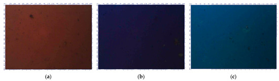
Figure 1.
Visual appearance of anodic TiO2 films obtained at (a) 10, (b) 15, and (c) 20 V.
Figure 2 shows a schematic diagram of the Carbon paste/TiO2/Ti/Al-based thin film structure used for the study.
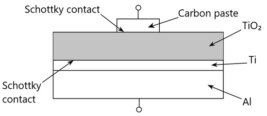
Figure 2.
Schematic diagram of the Carbon paste/TiO2/Ti/Al thin film structure.
Let us consider the metal–titanium oxide contact. As a result of the contact between the metal and titanium oxide, the near-surface region of the oxide will be depleted of the majority charge carriers (electrons). A space charge region forms on the titanium oxide side of the contact, creating a blocking contact or a Schottky barrier [20,21]. In structures with a Schottky barrier, the entire external voltage will be applied across the space charge region because the charge carrier concentration in this region is significantly lower than in other regions. A change in the voltage applied to the Schottky barrier leads to a change in the charge and width of the depletion region, which is reflected in the IVCs of the Schottky barrier structures.
In the structures used in our experiments, there are two metal/titanium oxide interfaces (Figure 2). Therefore, such a structure can be represented as a structure with two Schottky barriers connected in opposite directions. Furthermore, these Schottky barriers are technologically integrated with the base layer of n-type conductivity titanium oxide.
When analyzing the results obtained, the following features of the properties of anodic oxides must be taken into account. Anodic oxide films are formed on metals during their anodic polarization in electrolyte solutions and are similar in many physical properties to oxide films formed during thermal oxidation. At the same time, they differ in their structure. As a result of anodization, a two-layer oxide film is formed on the metal, in which the inner layer, adjacent to the metal, consists of a stoichiometric oxide, and the outer layer of oxide, bordering the electrolyte, contains residues of anions from the anodizing acid that act as donors [22,23]. At the interface with a metal, for the oxide layer containing electrolyte anions, the space charge region also incorporates the charge of ionized donors. Therefore, the Schottky barrier at this interface will be higher than at the metal/titanium oxide interface without embedded electrolyte anions. These anodic oxides in metal oxide metal (MOM), metal oxide semiconductor (MOS), and metal oxide electrolyte (MOE) systems exhibit conductivity asymmetry due to their two-layer structure [24]. Also, anodic oxides are amorphous oxides.
Figure 3 shows a typical two-dimensional AFM surface morphology of anodic TiO2 film. As can be seen, the TiO2 film is continuous and exhibits a uniform surface structure. The height of the surface features of the anodic TiO2 film is approximately 60 nm, and this is related to the fine-grained surface of the underlying 100 nm thick aluminum film, which was deposited by magnetron sputtering.
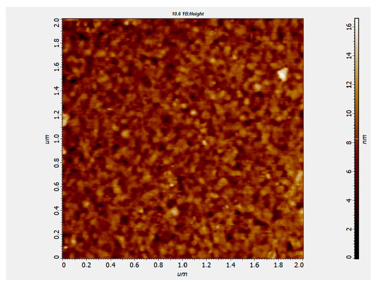
Figure 3.
Two-dimensional AFM surface morphology of anodic TiO2 films obtained at 10 V.
Figure 4 shows the forward and reverse I-V curves of a 14 nm thick anodic TiO2 film with a voltage sweep up to 0.5 V for sample temperatures starting from room temperature and decreasing into the low-temperature region.
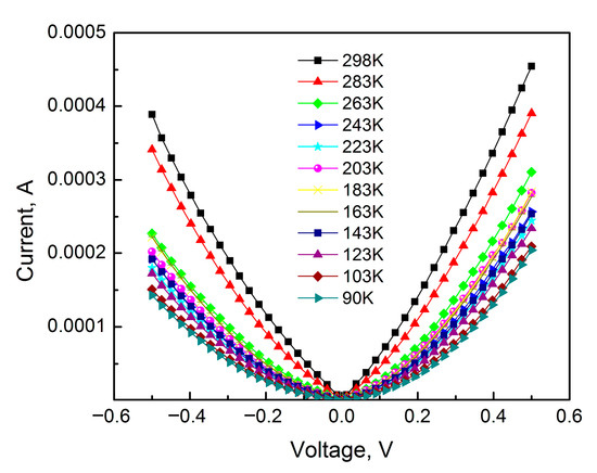
Figure 4.
IV characteristics of anodic TiO2 film (14 nm) under forward and reverse bias. Sample temperature: 298, 283, 263, 243, 223, 203, 183, 163, 143, 123, 103, and 90 K, maximum voltage 0.5 V.
As can be seen from Figure 4, the current–voltage characteristic of anodic TiO2 film has a complex nature. The IVCs in the forward (negative potential on the Ti electrode—cathodic polarization) and reverse (positive potential on the Ti electrode—anodic polarization) bias of the thin film structure are not symmetrical. The observed slight conductivity asymmetry in the Metal–TiO2–Ti system can be explained by the rectifying properties of anodic TiO2 film. In such systems, the anodic connection of the anodized metal is reversed (positive on Ti). As is known, anodic oxides exhibit conductivity asymmetry, i.e., they have rectification properties. It should be noted that in an MOS system with anodic oxide as a dielectric, the conductivity asymmetry depends on where the semiconductor is located, in place of the base electrode or as a counter electrode. In the MOS system, the IVCs exhibit significant asymmetry with a high rectification ratio when the semiconductor acts as the counter electrode.
Using the data from Figure 4 for the IVCs with different sample temperatures, the rectification ratios were calculated at bias voltages of 0.4 and 0.5 V, the results of which are shown in Figure 5.
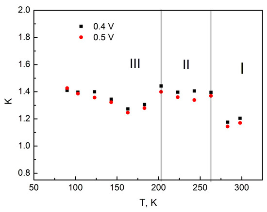
Figure 5.
Change in the rectification coefficient of anodic TiO2 film (14 nm) in the temperature range from 298 to 90 K.
The analysis of the character of the rectification ratio change in the considered temperature range (Figure 5) allowed us to identify three different sections, distinguished by their behavior.
Section I—Temperature range from 298 to 263 K. The rectification ratio in this section has values of 1.14–1.2. Section II—Temperature range from 263 to 203 K. The rectification ratio in this section has values of 1.34–1.44. Section III—Temperature range from 183 to 90 K. In this section, as the temperature decreases, there is a monotonous increase in the rectification ratio from 1.27–1.3 to 1.41–1.43.
It can be assumed that the observed features In anodic TiO2 film, related to the change in the rectification ratio with decreasing temperature, are caused by different conduction mechanisms.
To more clearly see how the nature of the conduction mechanism changes with decreasing temperature and how this is reflected in the I-V characteristics of anodic TiO2 film, the sample’s I-V curves at various temperatures were grouped into three categories according to the proposed division.
As is known, the main conduction mechanism can be identified by constructing I-V characteristics in coordinates that highlight linear regions, which can be attributed to a specific conduction mechanism. Figure 6 shows the IVC of the sample in ordinary and double logarithmic coordinates for Section I. As can be seen from Figure 6, the IVC in this section is highly dependent on temperature, which is characteristic of space–charge–limited currents (SCLC) since the degree of trap filling depends on temperature [14]. When considering the IVC of TiO2 films, it should be taken into account that at low voltages, the density of injected free charges is less than the density of intrinsic charge carriers, and therefore, Ohm’s law prevails. Consequently, ohmic conductivity takes place near the zero bias point. Therefore, for the analysis, voltages with a value higher than 0.06 V were used when the density of injected free charge carriers became greater than the density of intrinsic charge carriers. As can be seen, the experimental points are well approximated by a linear function in the logarithmic scale. This behavior of the dependence of current on bias voltage is characteristic of SCLC. Consequently, the conductivity mechanism in Section I is determined by SCLC. The IVC in this section is described by a power-law dependence of current on voltage J∞Um with m values equal to 1.24; 1.34 and 1.52 (positive region) and 1.21; 1.33 and 1.47 (negative region) for sample temperatures of 298, 283, and 263 K, respectively.
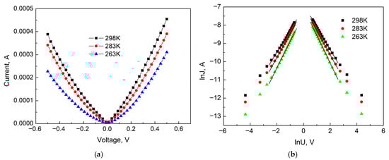
Figure 6.
IV characteristics of anodic TiO2 film (14 nm) under forward and reverse bias in ordinary (a) and double logarithmic coordinates (b). Sample temperature: 298, 283, and 263 K (Section I), maximum voltage 0.5 V.
It should be taken into account that in an amorphous dielectric, the traps are not monoenergetic and are distributed across energies. SCLC in a dielectric with traps exponentially distributed in energy [25,26] are related to the voltage by the following expression:
where Nc is the effective density of quantum states in the conduction band of the titanium oxide, ε is the relative dielectric permittivity of TiO2 film, ε0 is the electric constant, µ is the electron mobility, Nt is the concentration of traps in TiO2 film, e is the electron charge. This expression allows determining the exponent from the slope of the IVC in the double logarithmic scale (m) according to (l = m − 1) and then calculating the characteristic energy of trap distribution E0 using the expression:
The values of E0 are 6.2, 8.3 and 12.0 meV (positive region) and 5.4; 8.1 and 11.0 meV (negative region) for sample temperatures of 298, 283, and 263 K, respectively. As the temperature decreases, the energy E0 increases, which indicates a decrease in the Fermi level (increase in energy), since the degree of trap filling decreases as the temperature decreases. The Fermi level (F) is related to the characteristic energy by the following relation:
where ε is the relative dielectric permittivity of TiO2 film, ε0 is the electric constant, L is the thickness of TiO2 film, Nt is the concentration of traps in TiO2 film, and U is the applied voltage.
Consider the IVCs for Section II in the temperature range from 243 K to 203 K. Figure 7 shows the IVC of the sample for Section II in ordinary and double logarithmic coordinates.
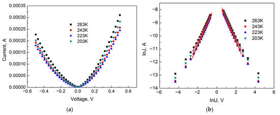
Figure 7.
IV characteristics of anodic TiO2 film (14 nm) under forward and reverse bias in ordinary (a) and double logarithmic coordinates (b). Sample temperature: 263, 243, 223, and 203 K (Section II), maximum voltage 0.5 V.
The IVC in this section is described by a power-law dependence of current on voltage J∞Um with m values equal to 1.52; 1.62; 1.65 and 1.55 (positive region) and 1.46; 1.63; 1.62 and 1.55 (negative region) for sample temperatures of 263, 243, 223, and 203 K, respectively.
The values of E0 are 12.0; 13.0; 12.0 and 10.0 meV (positive region) and 11.0; 13.0; 12.0 and 10.0 meV (negative region) for sample temperatures of 263, 243, 223 and 203 K, respectively. It can be noted that the different biasing of the TiO2 film does not affect the energy E0. It fluctuates within a narrow range between the values of 13.0 and 10.0 meV and, thus, weakly depends on the sample temperature.
Figure 8a shows the dependence of the energy E0 on the sample temperature. As is known, the bottom of the conduction band for an amorphous dielectric is blurred, and the tail of the conduction band extends deep into the forbidden band. Instead of the bottom of the conduction band, the edge of the conduction band is indicated in the diagram. When a voltage is applied to the sample, injected electrons are captured by traps, and all traps below the Fermi level will be filled (Figure 8b).
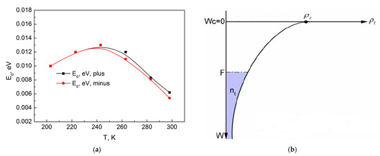
Figure 8.
Dependence of the energy E0 on the sample temperature under forward and reverse bias of TiO2 film (a), and the energy band diagram for an amorphous dielectric with traps filled with electrons below the Fermi level F (b).
As the temperature decreases, due to the decrease in the degree of trap filling, the number of electrons captured on the traps decreases, and the energy of the Fermi level and the characteristic energy E0 should increase, as seen from Figure 8b. At the same time, the slowing down of the increase in the energy E0 with decreasing temperature, followed by a smooth transition to its decrease, indicates the appearance of additional electrons on the traps, which are not related to the injection of electrons from the electrode but, for example, can be injected from donor levels. Consequently, the change in the behavior of the energy E0 after T = 263 K indicates the appearance of another conductivity mechanism. Therefore, Section II with the temperature range from 243 K to 203 K is the beginning of the conductivity mechanism involving donors for the case when the concentration of electrons on the traps is much greater than the electrons in the conduction band.
It can be noted that the IVCs in Section II are characterized by a weak temperature dependence, which is typical for currents with the Poole–Frenkel mechanism, and therefore Poole–Frenkel coordinates were chosen for the analysis. As is known, the IVC for the Poole–Frenkel effect is described by the following expression in Poole–Frenkel coordinates [26]:
where I—current flowing in the film, U—bias voltage, β—Poole–Frenkel constant, r—parameter in the equation, kB—Boltzmann constant, T—sample temperature in Kelvin, L—film thickness
The Poole–Frenkel constant is found from the following expression:
where e—electron charge, ɛ—high-frequency dielectric permittivity, and ɛ0—electric constant. For amorphous TiO2 ɛ = 80, тoгдa β = 1.34 × 10⁻²⁴.
Figure 9a shows the IVC of the sample with temperatures of 263 and 203 K for Section II in the coordinates of the logarithm of conductivity versus the square root of voltage. As can be seen, the linear section on the graph for forward bias does not appear immediately, but only after the voltage reaches a value of 0.24 V. In the case of reverse bias, the linear section arises for voltages above 0.27 V. From Figure 9a, we find that the tangent of the slope (m) of the approximating curves (linear form) for T = 263 K is 1.78 (forward bias (minus on Ti)) and 1.86 (reverse bias (plus on Ti)) and for T = 203 K is 1.74 (forward bias) and 2.15 (reverse bias). Accordingly, the parameter r (ɛ = 80) for T = 203 K is 2.07 (forward bias) and 1.98 (reverse bias), and for T = 203 K is 2.12 (forward bias) and 1.72 (reverse bias). Since the value of the parameter r is close to 2, in this case, there is an anomalous Poole–Frenkel effect, which describes the behavior of the donor level in the presence of shallow traps. Small traps are located above the donor centers. Also kB T > (—characteristic energy of donors), and therefore the donor band acts as one monoenergetic level, coinciding with the maximum density of the donor band. Donor centers in anodic TiO2 can be anionic (oxygen) vacancies due to their low formation energy [8,27].
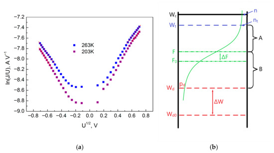
Figure 9.
IV characteristics of anodic TiO2 film (14 nm) under forward and reverse bias in Poole–Frenkel coordinates (a), and the energy band diagram for an amorphous dielectric with shallow traps located above the donor level (b). Sample temperature: 263 and 203 K (Section II), maximum voltage 0.5 V.
In an electric field, the ionization energy of the donor decreases, which is equivalent to reducing the distance from the bottom of the conduction band to the donor level. In the presence of shallow traps, the Fermi level shifts towards the bottom of the conduction band twice as slowly as the donor level (anomalous Poole–Frenkel effect). This is due to the fact that some electrons from the donors are thrown not only into the conduction band but also onto the overlying traps (Figure 9b).
For the Poole–Frenkel effect in the case of traps exponentially distributed in energy, the parameter r is related to the characteristic energy of the trap distribution across energies E0 according to the expression:
Then, at T = 263 K, E0 equals 0.021 eV (forward bias) and 0.023 eV (reverse bias), and for T = 203 K, E0 equals 0.016 eV (forward bias) and 0.024 eV (reverse bias). The results obtained show that at a sample temperature of T = 203 K, the characteristic energy E0 begins to be influenced by field effects under forward and reverse bias.
Figure 10 shows the IVC of the sample for Section III in ordinary coordinates and in the coordinates of the logarithm of conductivity versus the square root of voltage (Poole–Frenkel coordinates). From Figure 10b, we find that the tangent of the slope (m) of the approximating curves for T = 183 K is 2.19 (forward bias) and 2.57 (reverse bias), and for T = 90 K is 2.57 (forward bias) and 3.65 (reverse bias).
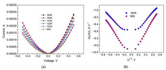
Figure 10.
IV characteristics of anodic TiO2 film (14 nm) under forward and reverse bias in ordinary coordinates (a) and Poole–Frenkel coordinates (b). Sample temperature: 183, 163, 143, 123, 103, and 90 K (Section III), maximum voltage 0.5 V.
Accordingly, the parameter r (ɛ = 80) for T = 183 K is 3.37 (forward bias) and 3.84 (reverse bias), and for T = 90 K is 7.93 (forward bias) and 8.84 (reverse bias).
Since the parameter r has a value greater than 2, this indicates that the level of traps and donors is not monoenergetic but blurred in the form of exponential “tails,” which is typical for amorphous dielectrics. If the blurring is large
> kB T, then only the upper part of the donor band is involved, i.e., only the upper tail of the donors. For this case, the parameter r is related to the characteristic energy distribution of donors across energies
and the characteristic energy distribution of traps across energies E0 according to the expression:
Then, at T = 183 K,
equals 2.27 E0 (forward bias) and 2.84 E0 (reverse bias), and for T = 90 K,
equals 6.93 E0 (forward bias) and 7.84 E0 (reverse bias).
Thus, the analysis of IVCs in Sections II and III and charge transport mechanisms shows that, in the forbidden band of anodic TiO2, in addition to traps, there are also donor centers, which agrees well with [27,28]. It can be noted that the donor centers are located below the level of traps in the forbidden band.
The observed decrease in the characteristic energy for donors is explained by the manifestation of field effects. The different behavior of the characteristic energy with different biasing indicates the presence of regions with different electric field strengths in the TiO2 film, which is associated with the two-layer structure of the anodic film [28]. With forward bias of anodic TiO2 film (cathodic polarization, minus on Ti), electrons from localized states in the region near the external electrode (positive potential) go to the positively charged electrode. Therefore, in anodic TiO2 film with this biasing, the electric field is more uniform and close to the applied external field. With reverse bias of anodic TiO2 film (anodic polarization, plus on Ti), due to the injection of electrons into deep traps in the near-electrode region (external electrode, negative potential), the magnitude of the electric field at the metal-oxide interface decreases significantly and will be less than the strength of the applied electric field. This also means that the configuration of the electric field changes in such a way that the field strength in the central part of the anodic TiO2 film increases. Consequently, when an external field is applied, on the energy diagram (near-electrode region near the external electrode), the shift in the donor level upward to the bottom of the conduction band will be greater with forward bias than with reverse bias due to the greater magnitude of the electric field strength. This agrees well with our results:
= 2.27E0 at T = 183 K (forward bias) and
= 2.84E0 (reverse bias). In the case of lowering the temperature, fewer electrons will be ionized at the donor centers. Therefore, all the above-described processes will be repeated, only at a greater depth in the forbidden band.
3. Materials and Methods
Aluminum films with a thickness of 100 nm and Ti films with a thickness of 50–60 nm were deposited on silicon (sample size 10 × 27 mm) and glass (10 × 27 mm) substrates by magnetron sputtering in an argon atmosphere (Magnetron sputtering unit model IzoLab from Izovac, Belarus). Prior to the vacuum deposition process, the prepared samples were chemically treated by heating in isopropyl alcohol at 60 °C for 10 min, then washed with distilled water and dried in a desiccator at 60 °C. The following parameters were used to deposit the aluminum films: source power 1.5 kW, discharge voltage—380 V, discharge current—3.7 A, argon pressure—6 × 10⁻² Pa, residual pressure in the chamber—10−3 Pa, film deposition rate—2.8 nm s−1. The Ti film deposition parameters were as follows: source power—1.0 kW, discharge voltage—310 V, discharge current—3.0 A, argon pressure—2 × 10⁻² Pa, residual pressure in the chamber—10−3 Pa, film deposition rate 0.1 nm s−1, substrate temperature—room temperature, distance between target and substrate—11 cm.
Electrochemical oxidation of the Ti films was carried out in an electrolyte based on a mixture of 2% aqueous oxalic acid solution and 1% aqueous sulfamic acid solution (by weight). A P-5827M potentiostat (Measuring Instruments Plant, Gomel, Belarus) was used as a current and voltage source for the titanium anodization processes. A two-electrode anodization cell was used with a titanium anode (sample with Ti film) and a graphite cathode. The set voltage value of the potentiostat determined the final thickness of the formed TiO2 film due to the self-regulating process of Ti anodization. Electrochemical oxidation of Ti was carried out in an electrolyte at a voltage of 10 V, followed by holding until the anodization current completely decayed (holding time: 1 min). An LEF-ZM-1 ellipsometer (λ = 632.8 nm) was used to measure the thickness of the TiO2 film. These studies were carried out with titanium films sputtered onto silicon substrates. The measurement results showed that the thickness of anodic TiO2 oxide was 14 nm. This value is in good agreement with the literature data [29] for the formation factor of anodic titanium oxide, 1.4 nm V−1. The thickness values of anodic titanium oxide films follow a linear behavior with anodizing voltage. After the anodization process, the samples were washed with distilled water and isopropyl alcohol. Then they were heated to 80 °C to remove residual water and stabilize the film structure.
The surface morphology was characterized using tapping-mode atomic force microscopy (NTEGRA PRIMA™, NT-MDT BV, Apeldoorn, The Netherlands) equipped with a probe VIT_P (NT-MDT BV, Apeldoorn, The Netherlands) with an NSG01 probe. To measure the current–voltage characteristics (IVCs), Carbon paste contacts (with a diameter of d ≈ 2 mm) were applied to the surface of the TiO2 films, and the Ti/Al layer served as the second contact.
IVCs of the samples, placed on a holder of an OPTCRYO198 optical flow nitrogen cryostat (LTLab, Inc. Fukuoka, Japan) with temperature stabilization, were measured at direct current in a nitrogen atmosphere in the temperature range T = 80–300 K in 10 K steps using an automated measurement setup based on a Keithley 6487 picoammeter (Keithley Instruments, Inc., Solon, OH, USA). The voltage was varied with a variable step in the range from −0.5 V to +0.5 V. Electrical contacts to the samples were made using silver wire, which was attached to the metal electrodes with carbon or silver paste (SPI).
4. Conclusions
The work investigated the IV characteristics of anodic TiO2 films obtained by electrochemical oxidation of Ti at a voltage of 10 V (film structure Me-TiO2-Ti-Al) in the temperature range T = 80–300 K with a bias voltage from −0.5 V to +0.5 V. The obtained data for different temperatures showed that the IV characteristics of anodic TiO2 film (14 nm) have a complex behavior. The IV curves in the forward (negative potential on the Ti electrode) and reverse (positive potential on the Ti electrode) biasing of the film structure are not symmetrical, although the observed conductivity asymmetry is insignificant. The nature of the change in the rectification coefficient for the film structure with anodic TiO2 film (14 nm) in the temperature range from 298 to 90 K and the dependence of the logarithm of the current on the inverse temperature allowed us to identify three temperature groups (sections) in which the IV characteristics differ in their behavior: Section I—temperature range from 298 to 263 K; Section II—temperature range from 263 to 203 K; Section III—temperature range from 183 to 90 K.
By constructing IV curves in coordinates that allow identifying linear sections with a specific conductivity mechanism, the IV characteristics in these sections were analyzed to find the conductivity mechanism. The analysis of conductivity mechanisms showed that anodic TiO2 is an n-type semiconductor, in the forbidden band of which there are both electron traps and donor centers formed by anionic (oxygen) vacancies. The consideration of the IV characteristics revealed that the conductivity mechanism in Section I is determined by SCLC. The IV characteristics in this section are described by a power-law dependence of current on voltage J∞Um. Section II in the temperature range from 243 to 203 K is characterized by the beginning of conductivity involving donor centers, for the case when the concentration of electrons at traps is much greater than the electrons in the conduction band. The IV characteristics in Section II have a weak temperature dependence, which is characteristic of currents with the Poole–Frenkel mechanism. The calculated values of the parameter r for the IV characteristics in this section were approximately equal to 2. This indicates that there is an anomalous Poole–Frenkel effect, which describes the behavior of the donor level in the presence of shallow traps.
In Section III in the temperature range from 183 to 90 K, the Poole–Frenkel conductivity mechanism takes place. Analysis of the IVCs in Poole–Frenkel coordinates showed that the parameter r in this case was greater than 2. This indicates that the levels of traps and donors are not monoenergetic, but are blurred in the form of exponential tails, which is characteristic of amorphous dielectrics. Thus, the analysis of IVCs in Sections II and III and charge transport mechanisms shows that, in the forbidden band of anodic TiO2, in addition to traps, there are donor centers. These donor centers are located below the level of traps in the forbidden band. It was concluded that the different behavior of the characteristic energy with different biasing of samples in the case of the Poole–Frenkel mechanism indicates the presence of regions in TiO2 film with different electric field strengths, which is associated with the two-layer structure of anodic film. It has shown that when an external field is applied on the energy diagram (near-electrode region near the external electrode) the shift in the donor level upward towards the bottom of the conduction band with forward bias is greater than with reverse bias due to the greater magnitude of the electric field strength (the local field adds up with the external field).
Author Contributions
Conceptualization, I.A.V.; methodology, I.A.V., V.A.M. and A.A.R.; software, I.A.V., V.A.M. and A.A.R.; validation, E.N.M., V.A.M. and I.A.V.; formal analysis, I.A.V., A.I.M. and A.A.R.; investigation, I.A.V., E.N.M., A.Y.G. and A.I.M.; resources, D.A.K.; data curation, E.N.M.; writing—original draft preparation, I.A.V.; writing—review and editing, E.N.M.; visualization, I.A.V.; supervision, E.N.M.; project administration, V.A.M.; funding acquisition, V.A.M. and D.A.K. All authors have read and agreed to the published version of the manuscript.
Funding
Investigations of surface morphology were carried out using an NTEGRA PRIMA™ microscope, supported by NT-MDT BV, the Netherlands. This research was funded by Belarusian Republication Foundation for Fundamentel Research grand number F25B-011.
Institutional Review Board Statement
Not applicable.
Informed Consent Statement
Not applicable.
Data Availability Statement
The original contributions presented in this study are included in the article. Further inquiries can be directed to the corresponding author.
Conflicts of Interest
Author Dmitry A. Kozodaev was employed by the company NT-MDT BV. The remaining authors declare that the research was conducted in the absence of any commercial or financial relationships that could be construed as a potential conflict of interest.
References
- Bulowski, W.; Szwanda, A.; Gawlińska-Nęcek, K.; Panek, P.; Lipiński, M.; Janusz-Skuza, M.; Szczerba, M.J.; Majchrowicz, Ł.; Mahapatra, A.; Prochowicz, D.; et al. Optimization of the ETL titanium dioxide layer for inorganic perovskite solar cells. J. Mater. Sci. 2024, 59, 7283–7298. [Google Scholar] [CrossRef]
- Zhao, Y.; Zhang, H.; Ren, X.; Zhu, H.L.; Huang, Z.; Ye, F.; Ouyang, D.; Cheah, K.W.; Jen, A.K.-Y.; Choy, W.C.H. Thick TiO2-Based Top Electron Transport Layer on Perovskite for Highly Efficient and Stable Solar Cells. ACS Energy Lett. 2018, 3, 2891–2898. [Google Scholar] [CrossRef]
- Hayali, A.; Alkaisi, M.M. High efficiency perovskite solar cells using DC sputtered compact TiO2 electron transport layer. EPJ Photovolt. 2021, 12, 8. [Google Scholar] [CrossRef]
- Ng, S.; Yam, F.K.; Sohimee, S.N.; Beh, K.P.; Tneh, S.S.; Cheong, Y.L.; Hassan, Z. Photoelectrochemical ultraviolet photodetector by anodic titanium dioxide nanotube layers. Sens. Actuators A Phys. 2018, 279, 263–271. [Google Scholar] [CrossRef]
- Lettieri, S.; Pavone, M.; Fioravanti, A.; Amato, L.S.; Maddalena, P. Charge Carrier Processes and Optical Properties in TiO2 and TiO2-Based Heterojunction Photocatalysts: A Review. Materials 2021, 14, 1645. [Google Scholar] [CrossRef]
- Liao, C.; Li, Y.; Tjong, S.C. Visible-Light Active Titanium Dioxide Nanomaterials with Bactericidal Properties. Nanomaterials 2020, 10, 124. [Google Scholar] [CrossRef]
- Feng, X.; Shankar, K.; Varghese, O.K.; Paulose, M.; Latempa, T.J.; Grimes, C.A. Vertically aligned single crystal TiO2 nanowire arrays grown directly on transparent conducting oxide coated glass: Synthesis details and applications. Nano Lett. 2008, 8, 3781–3786. [Google Scholar] [CrossRef]
- Hanaor, D.A.; Sorrell, C.C. Review of the anatase to rutile phase transformation. J. Mater. Sci. 2011, 46, 855–874. [Google Scholar] [CrossRef]
- Sarkar, A.; Khan, G.G. The formation and detection techniques of oxygen vacancies in titanium oxide-based nanostructures. Nanoscale 2019, 11, 3414–3444. [Google Scholar] [CrossRef]
- Liu, Z.; Zhong, X.; Walton, J.C.; Thompson, G.E. Anodic Film Growth of Titanium Oxide Using the 3-Electrode Electrochemical Technique: Effects of Oxygen Evolution and Morphological Characterizations. J. Electrochem. Soc. 2016, 163, E75–E82. [Google Scholar] [CrossRef]
- Sanchez, A.G.; Schreiner, W.; Duffó, G.; Ceré, S. Surface modification of titanium by anodic oxidation in phosphoric acid at low potentials. Part 1. Structure, electronic properties and thickness of the anodic films. Surf. Interface Anal. 2013, 45, 1037–1046. [Google Scholar] [CrossRef]
- Kang, K.W.; Limandri, S.P.; Castellano, G.; Suarez, S.G.; Trincavelli, J.C. Thickness determination of anodic titanium oxide films by electron probe microanalysis. Mater. Charact. 2017, 130, 50–55. [Google Scholar] [CrossRef]
- Sul, Y.T.; Johansson, C.B.; Jeong, Y.; Albrektsson, T. The electrochemical oxide growth behaviour on titanium in acid and alkaline electrolytes. Med. Eng. Phys. 2001, 23, 329–346. [Google Scholar] [CrossRef]
- Lausmaa, J.; Kasemo, B.; Mattsson, H.J.; Odelius, H. Multi-technique surface charaterization of oxide films on electropolished and anodically oxidized titanium. Appl. Surf. Sci. 1990, 45, 189–200. [Google Scholar] [CrossRef]
- Schneider, M.; Schroth, S.; Schilm, J.; Michaelis, A. Micro-EIS of anodic thin oxide films on titanium for capacitor applications. Electrochim. Acta 2009, 54, 2663–2671. [Google Scholar] [CrossRef]
- Yildiz, A.; Serin, N.; Kasap, M.; Serin, T.; Mardare, D. The thickness effect on the electrical conduction mechanism in titanium oxide thin films. J. Alloys Compd. 2010, 493, 227–232. [Google Scholar] [CrossRef]
- Rådegran, G.; Lausmaa, J.; Mattsson, L.; Rolander, U.; Kasemo, B. Preparation of ultra-thin oxide windows on titanium for TEM analysis. J. Electron Microsc. Tech. 1991, 19, 99–106. [Google Scholar] [CrossRef] [PubMed]
- Vattanasup, C.; Kuntiyaratana, T.; Rungsiyakull, P.; Chaijareenont, P. Color Formation on Titanium Surface Treated by Anodization and the Surface Characteristics: A Review. Chiang Mai Dent. J. 2023, 44, 13–21. [Google Scholar] [CrossRef]
- Weatherall, I.L. Interference colors of oxidized titanium metal surfaces. Color Res. Appl. 1992, 17, 352–355. [Google Scholar] [CrossRef]
- Ji, X.; Zuppero, A.; Gidwani, J.M.; Somorjai, G.A. The catalytic nanodiode: Gas phase catalytic reaction generated electron flow using nanoscale platinum titanium oxide Schottky diodes. Nano Lett. 2005, 5, 753–756. [Google Scholar] [CrossRef] [PubMed]
- Zhang, X.; Cai, W.; Zhang, J.; Brownless, J.; Wilson, J.; Zhang, Y.; Song, A. Solution-Processed TiO2-Based Schottky Diodes with a Large Barrier Height. IEEE Electron. Device Lett. 2019, 40, 1378–1381. [Google Scholar] [CrossRef]
- Vrublevsky, I.A.; Parkoun, V.; Sokol, V.A.; Schreckenbach, J.P. Analysis of chemical dissolution of the barrier layer of porous oxide on aluminum thin films using a re-anodizing technique. Appl. Surf. Sci. 2005, 252, 227–233. [Google Scholar] [CrossRef]
- Pashchanka, M. Conceptual Progress for Explaining and Predicting Self-Organization on Anodized Aluminum Surfaces. Nanomaterials 2021, 11, 2271. [Google Scholar] [CrossRef] [PubMed]
- Mibus, M.; Jensen, C.P.; Hu, X.; Knospe, C.; Reed, M.L.; Zangari, G. Dielectric breakdown and failure of anodic aluminum oxide films for electrowetting systems. J. Appl. Phys. 2013, 114, 014901. [Google Scholar] [CrossRef]
- Nespurek, S.; Zmeskal, O.; Sworakowski, J. Space-charge-limited currents in organic films: Some open problems. Thin Solid Film. 2008, 516, 8949–8962. [Google Scholar] [CrossRef]
- Weiser, K. Semiconductor Technique: Current Injection in Solids. In Science; Book Electrical Science Series; Lampert, M.A., Mark, P., Eds.; Academic Press: New York, NY, USA, 1970; Volume xiv, p. 354, illus. 18. [Google Scholar]
- Ardakani, H. Electrical and optical properties of in situ “hydrogen-reduced” titanium dioxide thin films deposited by pulsed excimer laser ablation. Thin Solid Film. 1994, 287, 280–283. [Google Scholar] [CrossRef]
- Brocklebank, M.; Feltham, H.; Noël, J.J. Mechanism of Titanium Electrochemical Oxidation Via Isotopic Labeling, High Resolution Ion Depth Profiling, and Impedance Spectroscopy. SSRN Electron. J. 2022, 435, 141342. [Google Scholar] [CrossRef]
- Schultze, J.W.; Stimming, U.; Weise, J. Capacity and Photocurrent Measurements at Passive Titanium Electrodes. Ber. Bunsenges. Phys. Chem. 1982, 86, 276–282. [Google Scholar] [CrossRef]


Disclaimer/Publisher’s Note: The statements, opinions and data contained in all publications are solely those of the individual author(s) and contributor(s) and not of MDPI and/or the editor(s). MDPI and/or the editor(s) disclaim responsibility for any injury to people or property resulting from any ideas, methods, instructions or products referred to in the content. |
© 2026 by the authors. Licensee MDPI, Basel, Switzerland. This article is an open access article distributed under the terms and conditions of the Creative Commons Attribution (CC BY) license.