Abstract
Diffractive optical elements (DOEs) offer significant advantages over conventional refractive optics, particularly in non-visible spectral regions such as ultraviolet, gamma rays, and X-rays, where material limitations restrict traditional optical components. Owing to their design flexibility, DOEs enable the generation of complex beam profiles—including circular, vortex, and Airy beams—across a wide range of wavelengths. Despite their structural simplicity and compatibility with micro- and nanoscale fabrication, conventional DOEs often suffer from limited focusing efficiency, frequently requiring additional refractive lenses that introduce optical aberrations, increased system complexity, and higher cost. In this work, we present an integrated design and fabrication approach for micro-scale diffractive optical elements capable of achieving high focusing performance without reliance on supplementary optical components. A machine learning-based decision tree method is employed to generate optimized writing paths, which are subsequently fabricated using direct laser lithography. The proposed integrated DOE structures enable efficient focusing of multiple customized beam profiles within a compact and standalone optical element. This approach improves optical efficiency while maintaining low fabrication cost and system simplicity. The demonstrated integrated micro-DOEs provide a scalable and versatile platform for advanced beam shaping and focusing applications in photonics, particularly where compactness and performance are critical.
1. Introduction
Diffractive optical elements (DOEs) are widely recognized as an effective solution for light manipulation in a broad range of optical applications. With high design flexibility, DOEs can generate complex beam profiles such as vortex beams, Bessel beams, and Airy beams, which are of considerable interest in fields including precision measurement, magnetic imaging, strong-field physics, and lithography [1,2,3,4,5,6,7,8]. Moreover, DOEs are particularly advantageous at non-visible wavelengths—such as ultraviolet, X-rays, and gamma rays—where the fabrication of conventional refractive optics is severely constrained by material limitations [9,10,11,12]. Despite these advantages, many conventional DOEs exhibit limited focusing capability and therefore require additional refractive lenses or auxiliary optical components to achieve well-defined focal intensity distributions. Previous studies have demonstrated the generation of ring-shaped foci, vortex beams, and Airy beams through combinations of DOEs with lenses, axicons, or other supporting optical elements [5,13,14,15,16]. While such hybrid configurations can improve beam shaping and focusing performance, they inevitably increase system complexity, size, and cost, and may introduce optical aberrations that degrade overall performance.
To overcome these limitations, integrating the focusing functionality directly into the DOE structure represents a promising strategy. In particular, Fresnel zone plates (FZPs) are well known for their intrinsic focusing capability and have been widely employed as lens alternatives in various optical systems [17]. By integrating the structural characteristics of an FZP with those of conventional DOEs, a new class of integrated DOEs can be realized that simultaneously shapes the beam profile and focuses light without reliance on additional optical components. Furthermore, the integration of multiple DOE functionalities within a single structure enables the generation of customized and application-specific beam profiles in a compact form factor.
A key challenge in realizing such integrated DOEs lies in their fabrication, as the resulting structures often involve complex geometries and fine feature details. Accurate translation of the designed phase or amplitude patterns into fabrication-ready writing paths is therefore essential. In this work, we present a complete and cost-effective workflow for the design and fabrication of complex-shaped DOEs, tailored for a custom-built, low-budget laser lithography system. The proposed approach combines Fourier optics-based DOE design methods—such as computer-generated holography (CGH) and iterative Fourier transform techniques [18,19,20,21]—with a machine learning decision tree technique (MLDTT) for writing-path generation, followed by direct laser lithography (DLL). The performance and reliability of DLL for DOE fabrication have been demonstrated in numerous previous studies [16,22,23,24,25], while MLDTT is well established as a non-parametric supervised learning method capable of efficiently handling classification and regression tasks [26,27]. In the present workflow, the MLDTT algorithm converts the numerical DOE matrix directly into optimized laser writing paths, determining regions to be processed or omitted with high precision. The entire design, path-generation, and fabrication process is implemented within a unified computational environment, minimizing software dependency and reducing potential sources of error. This integrated strategy enables the fabrication of compact, robust DOEs capable of independent beam shaping and focusing, with reduced fabrication time, labor, and cost. The resulting devices are well-suited for a wide range of optical applications, particularly at non-visible wavelengths where traditional refractive optics are impractical or prohibitively expensive.
2. Design Methodology and Numerical Matrix Generating
In this section, the design methodology for the proposed diffractive optical elements is presented, primarily based on CGH. The objective of this section is to design the DOE structures, predict their optical performance through numerical simulation, and generate the corresponding numerical matrices required for subsequent laser writing path generation. Several representative DOE types are investigated, including axicon zone plates (ZPs), axicon spiral zone plates (SZPs), and fork grating DOEs, to demonstrate the effectiveness and generality of the proposed approach.
The physical principles of holography have been comprehensively described by Goodman [28], in which hologram formation is explained as a two-step process consisting of recording and reconstruction. During the recording stage, an interference pattern is formed by the superposition of an object wave with an unknown phase and amplitude and a coherent reference wave with known characteristics (Figure 1). The resulting interference pattern encodes the information of the object wave. The sum of intensity of the interference generated by “object wave” a (x,y) = |a (x,y)| exp [−jø(x,y)] and “reference wave” A (x,y) = |A (x,y)| exp [−jψ(x,y)] (which object wave interferes) is calculated by
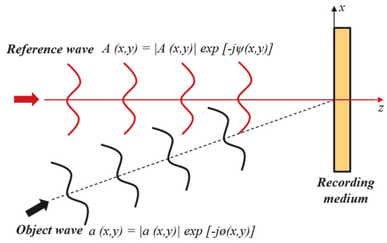
Figure 1.
Optical configuration for interferometric hologram recording.
After recording, the interference pattern is transferred to a photosensitive medium. Upon illumination with the reference wave, the hologram reconstructs the original object wave as well as its conjugate (virtual) wave, thereby reproducing the encoded optical field. CGH extends this concept into a numerical framework, in which the interference pattern is calculated computationally and encoded into a phase or amplitude distribution that can be represented in binary, multilevel, or grayscale formats. Detailed discussions on DOE formation using CGH can be found in previous studies [29]. From a theoretical perspective, CGH can be regarded as an interferogram resulting from the superposition of two wavefronts. As an illustrative example, the interference between a plane reference wave A (Equation (2)) and a conical wave B (Equation (3)), propagating at an angle θ along the z-direction (Figure 2a), produces an axicon zone plate pattern, provided that both waves have constant amplitudes:
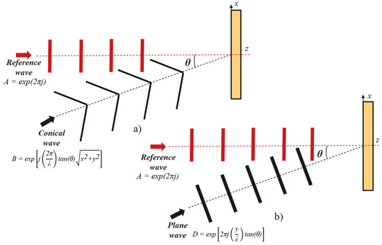
Figure 2.
(a) Superposition of a plane wave and a conical wave, resulting in an axicon zone plate (ZP). (b) Superposition of two plane waves, resulting in a linear grating pattern.
In this formulation, λ denotes the wavelength, and x and y represent the coordinates. The conical wavefront, which can be generated when a plane wave is incident on a refractive axicon, exhibits a linear phase variation along the radial direction, resulting in evenly spaced interference fringes. Similarly, a linear grating pattern (Figure 2b) can be obtained by replacing Equation (3) with Equation (4):
In the next stage, the binary classification process is applied:
An Axicon ZP (Figure 3a) is created with the circle focus shape. In a similar manner, many DOEs can be formed by this method. Additionally, we can combine Equation 3 with a spiral pattern as described in Equation (6):
where p is the topological charges, =, and the Axicon SZP (Figure 3b) is completed to enable the creation of vortex beams. A similar methodology can be employed to construct a Fork Grating DOE (Figure 3c) by integrating a spiral pattern with a linear grating as mentioned above. In addition, the Fork Grating DOE is effective in generating a vortex beam, which presents a viable alternative to the SZP in certain applications.
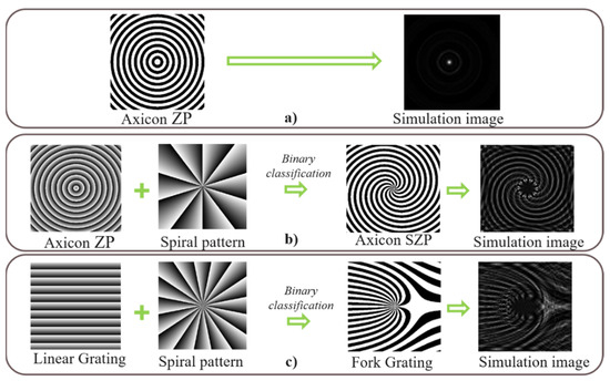
Figure 3.
DOE designs and their simulated optical performance: (a) Axicon ZP. (b) Axicon spiral zone plate (SZP). (c) Fork grating DOE.
To check the performance of the DOEs, we use the “Fresnel Impulse Response Propagator” approach (based on the condition of dimension, propagation distance, and different methods may be used depending on the above conditions if necessary). This method allows us to model the optical characteristics of every DOE by employing the theoretical framework provided by the Rayleigh–Sommerfeld diffraction solution I [30]:
whereas the Rayleigh-Sommerfield impulse response general form is
and
while the source complex field amplitude is , is the field retrieved after the source plane propagates a z (mm) distance and
The simulation results shown in Figure 3 indicate that the individual DOEs considered in this study are unable to achieve satisfactory focusing performance when operating independently. To overcome this limitation and enable the generation of well-defined intensity distributions, an FZP with identical aperture size, wavelength, and matrix dimensions is integrated with each DOE. This integration yields a new class of DOEs capable of simultaneously shaping the beam profile and focusing light. Although an FZP functions analogously to a refractive lens, its incorporation directly into the DOE structure significantly reduces system size and overall cost. This advantage is particularly important for non-visible wavelengths, such as X-rays, ultraviolet, and gamma rays, where the fabrication of conventional lenses is significantly more expensive and technologically challenging. The transmission function of the FZP is given by
where f is the FZP focal length and of the FZP, and in this research, it is always equal to 40 mm for every case. The integration of FZP with DOEs results in the formation of novel DOEs, significantly enhancing their focusing capabilities to achieve the desired intensity profile (Figure 4). Table 1 describes the parameters in the laboratory scale for each design below.
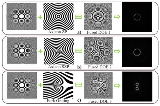
Figure 4.
Integrated DOE designs and their simulated optical performance after Fresnel zone plate (FZP) integration: (a) Axicon ZP. (b) Axicon SZP. (c) Fork grating DOE.

Table 1.
Fused DOEs parameters.
Figure 5 presents several representative integrated DOE designs along with their corresponding parameters. The characteristics of the generated beams can be tailored by adjusting parameters such as the DOE dimensions, the focal length of the integrated FZP, the axicon angle θ, and the topological charge. This tunability enables flexible customization of the beam properties to meet specific application requirements.
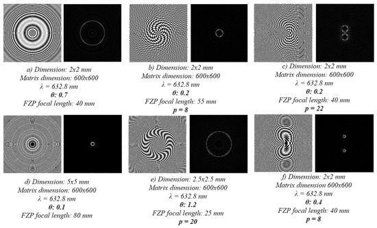
Figure 5.
Effect of design parameters on beam characteristics. An increase in the axicon angle θ leads to a larger beam size, whereas a decrease in θ results in a smaller beam, as shown in (a,b,d,e). An increase in the topological charge p produces a larger beam diameter, while increasing θ causes the dual beams to separate further, as illustrated in (c,f). The corresponding parameters are listed in Table 1.
Overall, the design process aims to encode the desired optical functionality into a numerical matrix representation while enabling accurate prediction of the resulting optical performance. The generated numerical matrices serve as direct inputs for laser writing path generation, which is described in the following section.
3. Fabrication Process
In the previous section, the designed DOEs are represented as numerical matrices, which are used directly to generate laser writing paths within the MATLAB R2020b environment. This integrated approach eliminates the need for supplementary software and enables precise control of relevant fabrication parameters, thereby improving overall system efficiency. The complete workflow is illustrated in Figure 6a.
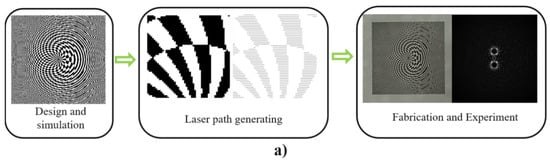
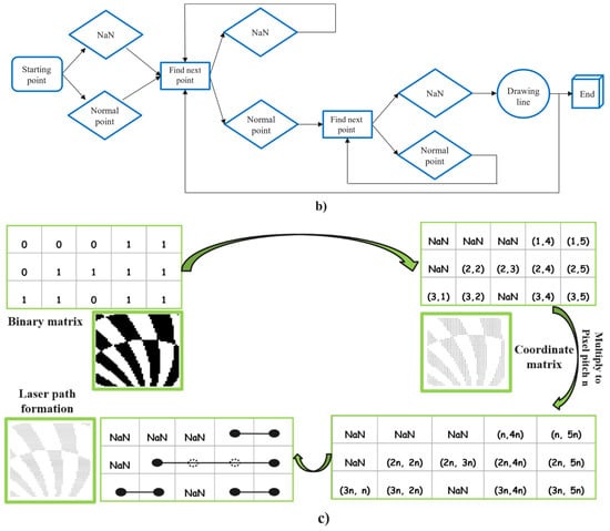
Figure 6.
(a) Overall workflow of DOE design, fabrication, and optical evaluation. (b) Logical flowchart of the laser writing path generation algorithm. (c) Formation of laser writing paths.
The laser writing path generation is based on an MLDTT, which employs a classification-based decision-making strategy. In the computational representation, each DOE is expressed as a binary matrix, where each element corresponds to a pixel with a value of either 0 or 1. Pixels with a value of 1 represent regions to be processed by the laser, while pixels with a value of 0 correspond to unprocessed regions. Based on this representation, the MLDTT algorithm determines the writing sequence by selectively connecting only the active pixels, enabling efficient and accurate writing path generation.
The numerical pixel positions are first converted into coordinate matrices corresponding to the DOE layout. Pixels with a value of 0 are classified as NaN (Not a Number), whereas pixels with a value of 1 are mapped as valid coordinate points for laser processing:
The resulting coordinate matrix is then scaled according to the pixel pitch defined in Table 1, converting the normalized coordinates into real-world dimensions compatible with the DLL system. Subsequently, the MLDTT algorithm scans each row or column, connecting valid points while ignoring NaN entries to optimize computation and reduce fabrication time, as illustrated in Figure 6b. The finalized writing paths are then transferred to the DLL system for fabrication (Figure 6c). All numerical calculations from the design stage (Section 2) to writing-path generation (Section 3) were executed in MATLAB on a personal laptop (Dell Latitude 7390, Dell Inc., Round Rock, TX, USA), Intel Core i7-8650U CPU @ 1.90 GHz, 16 GB RAM), with a typical computation time of several seconds per DOE.
A schematic diagram of the DLL system is shown in Figure 7a. An Ar+ laser source with a maximum output power of 1.5 W (1) generates the laser beam, whose intensity is modulated by an acousto-optic modulator (AOM) (2) controlled via a servo feedback system to ensure stable power output. A mechanical shutter (3) enables beam interruption when required. The beam is then directed by a set of mirrors (4–6) toward the laser writing head, which is equipped with an objective lens (100× magnification, numerical aperture of 0.7) (7). The sample (8) is mounted on high-precision motorized translation stages with a minimum step size of 10 nm, allowing controlled motion along the X and Y axes (9,10). All components are integrated through a centralized control system (11). During fabrication, the stage scanning speed was fixed at 0.1 mm/s, and the laser power at the sample plane was set to 9 mW.
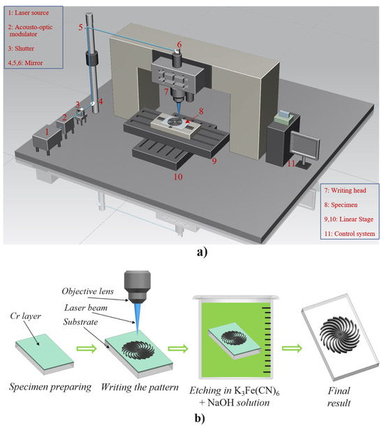
Figure 7.
(a) Schematic diagram of the DLL system. (b) Chemical etching process used for DOE fabrication.
The fabrication procedure using the DLL system is illustrated in Figure 7b. A glass substrate (refractive index ≈ 1.5) coated with a 70 nm thick chromium (Cr) layer was used as the starting material. The generated laser writing paths were imported into the DLL system to inscribe the designed patterns onto the Cr-coated surface. Under laser irradiation at a wavelength of 514.5 nm, the exposed Cr layer was locally converted into chromium(III) oxide (Cr2O3). Subsequently, a chemical etching process was performed for 5 min using an aqueous solution of K3Fe(CN)6 and NaOH to selectively remove the unexposed Cr layer while preserving the Cr2O3 regions. This process resulted in the final DOE structures.
The fabricated DOEs are shown in Figure 8. The images were captured using a commercial APS-C camera and lens to demonstrate the physical size of the devices relative to a standard ballpoint pen tip. Visual inspection indicates that all fabricated DOEs exhibit clean surfaces and structural features that closely match the designed patterns. A detailed surface analysis and quantitative characterization of the global and local surface profiles are presented in the following section to further evaluate fabrication consistency and accuracy.
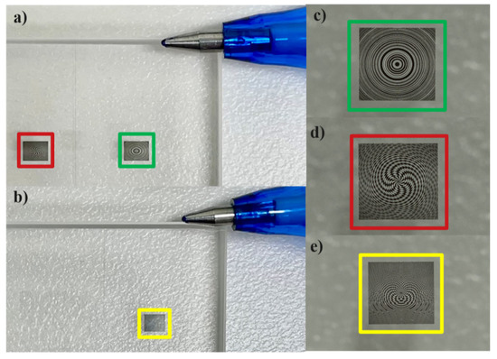
Figure 8.
Fabrication results of the DOEs: (a,b) Photographs of fabricated specimens. (c) Axicon ZP. (d) Axicon SZP. (e) Fork grating DOE.
4. Optical Verification and Results
In this section, the optical performance and surface quality of the fabricated diffractive optical elements are experimentally evaluated. Surface measurements were conducted using a white-light scanning interferometer (NV-2400 Nano System, NanoSystem, Daejeon, Republic of Korea) to assess the structural fidelity and surface roughness of the fabricated DOEs. In addition, a dedicated optical characterization setup was constructed to verify the focusing and beam-shaping performance of the devices, as illustrated in Figure 9.
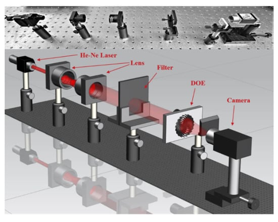
Figure 9.
Optical setup for experimental verification of DOE performance.
A He–Ne laser emitting at a wavelength of 632.8 nm was used as the coherent light source. To optimize the illumination conditions for the CMOS camera, the beam was expanded using a two-lens configuration combined with an optical filter for intensity adjustment. The optical system consisted of a Thorlabs AC254-030-A-ML lens (Thorlabs, Newton, NJ, USA)with a diameter of 25.4 mm and a focal length of 30 mm (BBAR coating for 400–700 nm, N-BAF10/N-SF6HT), followed by a Thorlabs AC254-300-A-ML lens with a focal length of 300 mm and a similar diameter (BBAR coating for 400–700 nm, N-BK7/SF2). The fabricated DOE samples were positioned in front of the CMOS camera on an adjustable translation stage to accurately capture the focal intensity distributions.
It is important to emphasize that no additional refractive lenses or auxiliary optical components were used to assist the focusing or beam shaping of the DOEs. As a result, the recorded intensity distributions directly reflect the intrinsic optical performance of the integrated DOEs. Figure 10, Figure 11 and Figure 12 present a comparative analysis of the surface quality measurements and the corresponding experimental intensity distributions for each DOE listed in Table 1. Furthermore, Figure 13 illustrates the two-dimensional and three-dimensional intensity maps of the generated beam patterns.
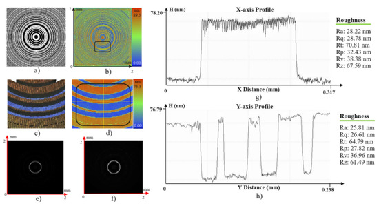
Figure 10.
Optical evaluation of the axicon ZP: (a) Simulation design. (b) Global surface measurement. (c,d) Local surface views. (e) Simulated intensity distribution. (f) Experimental intensity distribution. (g,h) Surface profiles along the X- and Y-axes in (d), including surface roughness information.
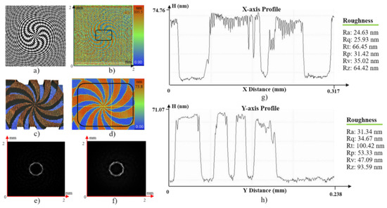
Figure 11.
Optical evaluation of the axicon SZP: (a) Simulation design. (b) Global surface measurement. (c,d) Local surface views. (e) Simulated intensity distribution. (f) Experimental intensity distribution. (g,h) Surface profiles along the X- and Y-axes in (d), including surface roughness information.
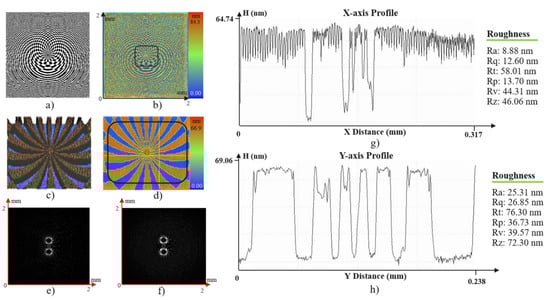
Figure 12.
Optical evaluation of the fork grating DOE. (a) Simulation design. (b) Global surface measurement. (c,d) Local surface views. (e) Simulated intensity distribution. (f) Experimental intensity distribution. (g,h) Surface profiles along the X- and Y-axes in (d), including surface roughness information.
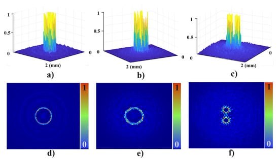
Figure 13.
Three-dimensional and two-dimensional intensity distributions of the experimental results: (a) 3D intensity map of Figure 10f. (b) 3D intensity map of Figure 11f. (c) 3D intensity map of Figure 12f. (d) 2D intensity map of Figure 10f. (e) 2D intensity map of Figure 11f. (f) 2D intensity map of Figure 12f.
The surface measurement results demonstrate high fabrication quality, with DOE geometries closely matching the designed patterns and exhibiting good surface uniformity. In addition, the experimentally observed intensity distributions show strong agreement with the numerical simulations. These results confirm that the integration of Fresnel zone plate functionality within the DOE structure effectively enhances focusing capability while simultaneously enabling precise modulation of the intensity distribution. The proposed fabrication approach has proven to be reliable for producing integrated DOEs with various micro-scale geometries.
The demonstrated method is applicable to a wide range of diffractive structures, including sector-based zone plates [31], square zone plates with chiral side lobes [32], and Airy beam generators. Owing to their compactness, mechanical robustness, lens-free operation, and low fabrication cost, the resulting DOEs are well-suited for practical optical systems. Furthermore, the integrated design strategy can be extended beyond FZP-based structures by combining multiple DOE functionalities, enabling diverse applications such as vortex beam generation for X-ray microscopy [33], transdermal drug delivery [34], Bessel beam generation for glass cutting [35], Airy beam formation [36], flat-top beam shaping [37], and square beam generation [38].
5. Conclusions
In this work, we have demonstrated a complete and cost-effective workflow for the design and fabrication of integrated DOEs using DLL, supported by Fourier optics methods and an MLDTT. The proposed approach enables the seamless transformation of numerically designed DOE patterns into fabrication-ready writing paths and their subsequent realization as physical devices.
The entire design and path-generation process is implemented within a single MATLAB-based environment, eliminating the need for expensive commercial software or auxiliary equipment. Combined with a maskless DLL system and a simple chemical etching process, the proposed method offers a practical and accessible solution for micro-scale DOE fabrication. Surface characterization results confirm the reliability and effectiveness of the manufacturing process, demonstrating that complex and high-resolution DOE structures can be produced with good optical quality.
The resulting integrated DOEs are capable of independently shaping and focusing light without reliance on additional optical components, thereby reducing system complexity, size, and cost. This flexibility allows the fabrication process to be readily adapted to different optical system requirements and beam configurations. Potential applications include the generation of vortex and Bessel beams, and broader use in areas such as semiconductor processing, sensing technologies, and CGH. Overall, the proposed strategy provides a scalable and versatile platform for advanced diffractive optics, particularly in applications where compactness and cost efficiency are critical.
Author Contributions
Conceptualization, H.T.D.T., Y.-S.G. and H.-G.R.; Methodology, H.T.D.T., Y.-S.G. and H.-G.R.; Software, H.T.D.T.; Validation, H.T.D.T., Y.-S.G. and H.-G.R.; Formal analysis, H.T.D.T., Y.-S.G. and H.-G.R.; Investigation, H.T.D.T. and H.-G.R.; Resources, H.-G.R.; Data curation, H.T.D.T.; Writing—original draft, H.T.D.T.; Writing—review & editing, Y.-S.G. and H.-G.R.; Visualization, H.T.D.T.; Supervision, H.-G.R.; Project administration, H.-G.R.; Funding acquisition, H.-G.R. All authors have read and agreed to the published version of the manuscript.
Funding
This work was supported in part by the Technology Innovation Program (Grant no. RS-2023-00237714, Development of Dynamic Metrology Tool for CMP Process Stabilization) funded By the Ministry of Trade, Industry & Energy (MOTIE, Korea) (Grant no. 1415187786) and in part by the Technology Innovation Program (20020311, Optical Technology for the Automatic Analysis of EUV Mask) funded by the Ministry of Trade, Industry & Energy (MOTIE, Korea).
Data Availability Statement
The data utilized in this study were obtained from the Korea Institute of Standards and Science (KRISS). Data are available from the authors upon request, and with permission from the Korea Institute of Standards and Science.
Conflicts of Interest
The authors declare that they have no known competing financial interests or personal relationships that could have appeared to influence the work reported in this paper.
References
- Wu, L.; Bai, Z.; Liu, R.; Wang, Y.; Yu, J.; Ran, J.; Chen, Z.; Luo, Z.; Liao, C.; Wang, Y.; et al. Polarization-Independent Focusing Vortex Beam Generation Based on Ultra-Thin Spiral Diffractive Lens on Fiber End-Facet. Photonics 2024, 11, 1167. [Google Scholar] [CrossRef]
- Kotlyar, V.V.; Nalimov, A.G.; Stafeev, S.S. Focusing a Vortex Laser Beam with Polarization Conversion. Photonics 2021, 8, 480. [Google Scholar] [CrossRef]
- Gao, H.; Hu, X.; Yang, Z.; Liu, Z. Application of vortex beam interference in displacement measurement. In Proceedings of the Fourteenth International Conference on Information Optics and Photonics (CIOP 2023), Xi’an, China, 24 November 2023; Volume 12953, p. 129352G. [Google Scholar] [CrossRef]
- Barrows, F.; Petford-Long, A.K.; Phatak, C. 3D magnetic imaging using electron vortex beam microscopy. Commun. Phys. 2022, 5, 324. [Google Scholar] [CrossRef]
- Khonina, S.N.; Kazanskiy, N.L.; Khorin, P.A.; Butt, M.A. Modern Types of Axicons: New Functions and Applications. Sensors 2021, 21, 6690. [Google Scholar] [CrossRef]
- Zhai, Z.; Cheng, Z.; Lv, Q.; Wang, X. Tunable Axicons Generated by Spatial Light Modulator with High-Level Phase Computer-Generated Holograms. Appl. Sci. 2020, 10, 5127. [Google Scholar] [CrossRef]
- Summers, A.M.; Yu, X.; Wang, X.; Raoul, M.; Nelson, J.; Todd, D.; Zigo, S.; Lei, S.; Trallero-Herrero, C.A. Spatial characterization of Bessel-like beams for strong-field physics. Opt. Express 2017, 25, 1646–1655. [Google Scholar] [CrossRef]
- Fan, D.; Wang, L.; Ekinci, Y. Nanolithography using Bessel Beams of Extreme Ultraviolet Wavelength. Sci. Rep. 2016, 6, 31301. [Google Scholar] [CrossRef]
- Soltau, J.; Meyer, P.; Hartmann, R.; Strüeder, L.; Soltau, H.; Salditt, T. Full-field x-ray fluorescence imaging using a Fresnel zone plate coded aperture. Optica 2023, 10, 127–133. [Google Scholar] [CrossRef]
- Marchesini, S.; Sakdinawat, A. Shaping coherent x-rays with binary optics. Opt. Express 2019, 27, 907–917. [Google Scholar] [CrossRef]
- Skinner, G.K. Design and imaging performance of achromatic diffractive–refractive x-ray and gamma-ray Fresnel lenses. Appl. Opt. 2004, 43, 4845–4853. [Google Scholar] [CrossRef] [PubMed]
- Feng, S.; Wang, Z.; Cheng, X.; Dun, X. Design of diffractive optical element for ultra-thin deep ultraviolet imaging system. In Proceedings of the International Conference on Optoelectronic and Microelectronic Technology and Application, Nanjing, China, 4 December 2020; Volume 11617, pp. 560–567. [Google Scholar]
- Nalimov, A.; Stafeev, S.; Kotlyar, V.; Kozlova, E. Optical Sensor Methodology for Measuring Shift, Thickness, Refractive Index and Tilt Angle of Thin Films. Photonics 2023, 10, 690. [Google Scholar] [CrossRef]
- Khonina, S.N.; Ustinov, A.V.; Kirilenko, M.S.; Kuchmizhak, A.A.; Porfirev, A.P. Application of a binary curved fork grating for the generation and detection of optical vortices outside the focal plane. J. Opt. Soc. Am. B 2020, 37, 1714–1721. [Google Scholar] [CrossRef]
- Kichi, Z.A.; Sabouri, S.G. Multiple Airy beam generation by a digital micro mirror device. Opt. Express 2022, 30, 23025–23034. [Google Scholar] [CrossRef]
- Sedova, V.; Ogor, F.; Rovera, J.; Tsilipakos, O.; Wiedenmann, J.; Heggarty, K.; Erdmann, A. Advances in modeling and optimization for two-photon lithography. J. Micro/Nanopatter. Mater. Metrol. 2025, 24, 023001. [Google Scholar] [CrossRef]
- Wang, Z.; Piao, M.; Xie, N.; Zhao, Y.; Zhang, C.; Ma, D.; Yang, D. Optimal design of the computational flat diffractive optical system. Opt. Express 2024, 32, 5969–5981. [Google Scholar] [CrossRef]
- Dallas, W.J. Computer-Generated Holograms. In Digital Holography and Three-Dimensional Display; Poon, T.C., Ed.; Springer: Boston, MA, USA, 2006. [Google Scholar] [CrossRef]
- Feldman, M.R.; Guest, C.C. Computer generated holographic optical elements for optical interconnection of very large scale integrated circuits. Appl. Opt. 1987, 26, 4377–4384. [Google Scholar] [CrossRef] [PubMed]
- Wyrowski, F.; Bryngdahl, O. Iterative Fourier-transform algorithm applied to computer holography. J. Opt. Soc. Am. A 1988, 5, 1058–1065. [Google Scholar] [CrossRef]
- Hacker, M.; Stobrawa, G.; Feurer, T. Iterative Fourier transform algorithm for phase-only pulse shaping. Opt. Express 2001, 9, 191–199. [Google Scholar] [CrossRef]
- Trung, H.T.D.; Nguyen, H.L.V.; Munnibee, A.; Kim, Y.-J.; Ghim, Y.-S.; Rhee, H.G. Design and fabrication of a Fresnel zone plate with an enhanced depth of focus. Appl. Opt. 2024, 63, 6384–6392. [Google Scholar] [CrossRef]
- Zeitner, U.D.; Banasch, M.; Trost, M. Potential of E-beam lithography for micro- and nano-optics fabrication on large areas. J. Micro/Nanopatter. Mater. Metrol. 2023, 22, 041405. [Google Scholar] [CrossRef]
- Smith, M.A.; Berry, S.; Parameswaran, L.; Holtsberg, C.; Siegel, N.; Lockwood, R.; Chrisp, M.P.; Freeman, D.; Rothschild, M. Design, simulation, and fabrication of three-dimensional microsystem components using grayscale photolithography. J. Micro/Nanolithogr. MEMS MOEMS 2019, 18, 043507. [Google Scholar] [CrossRef]
- Stonyte, D.; Jukna, V.; Lukosiunas, I.; Zakarauskas, P.; Huang, H.-H.; Katkus, T.; Zheng, N.; Le, N.H.A.; Juodkazis, S.; Gailevicius, D.; et al. Four-level diffractive photon sieves by deep-UV femtosecond laser ablation. Opt. Express 2024, 32, 43102–43117. [Google Scholar] [CrossRef]
- Rahman, M.; Kamal, N.; Abdullah, N.F. EDT-STACK: A stacking ensemble-based decision trees algorithm for tire tread depth condition classification. Results Eng. 2024, 22, 102218. [Google Scholar] [CrossRef]
- Alrbai, M.; Al-Dahidi, S.; Alahmer, H.; Al-Ghussain, L.; Hayajneh, H.; Shboul, B.; Abusorra, M.; Alahmer, A. Utilizing waste heat in wastewater treatment plants for water desalination: Modeling and Multi-Objective optimization of a Multi-Effect desalination system using Decision Tree Regression and Pelican optimization algorithm. Therm. Sci. Eng. Prog. 2024, 54, 102784. [Google Scholar] [CrossRef]
- Goodman, J.W. Introduction to Fourier Optics, 2nd ed.; McGraw-Hill Companies Inc.: New York, NY, USA, 1996. [Google Scholar]
- Vijayakumar, A.; Bhattacharya, S. Design and Fabrication of Diffractive Optical Elements with MATLAB.; SPIE-Press: Bellingham, WA, USA, 2017; ISBN 9781510607064. [Google Scholar] [CrossRef]
- Voelz, D.G. Computational Fourier Optics: A MATLAB Tutorial; SPIE-Press: Bellingham, WA, USA, 2011; Volume TT89, pp. 52+64–66. ISBN 9780819482044. [Google Scholar]
- Torcal-Milla, F.J.; Sanchez-Brea, L.M.; Gomez-Pedrero, J.A. Sector-based Fresnel zone plate with extended depth of focus. Opt. Laser Technol. 2022, 154, 108294. [Google Scholar] [CrossRef]
- Vijayakumar, A.; Vinoth, B.; Minin, I.V.; Rosen, J.; Minin, O.V.; Cheng, C.-J. Experimental demonstration of square Fresnel zone plate with chiral side lobes. Appl. Opt. 2017, 56, F128–F133. [Google Scholar] [CrossRef]
- Sakdinawat, A.; Liu, Y. Soft-x-ray microscopy using spiral zone plates. Opt. Lett. 2007, 32, 2635–2637. [Google Scholar] [CrossRef]
- Li, Y.; Guo, M.; Guo, G.; Ma, Q. Transdermal drug delivery mediated by acoustic vortex beam. Ultrasonics 2024, 140, 107304. [Google Scholar] [CrossRef] [PubMed]
- Liang, G.; Sun, S.; Wang, J.; Qu, Z.; Wei, T.; Liu, X.; Sun, H.; Monka, P.P.; Hamza, A. Application of array Bessel beam generated by superposition method in electronic glass cutting. Opt. Lasers Eng. 2024, 181, 108384. [Google Scholar] [CrossRef]
- Trung, H.T.D.; Ghim, Y.-S.; Rhee, H.G. Design and Fabrication of Micro-binary Diffractive Optical Elements to Generate Airy Beams Using a Versatile Direct Laser Lithography Machine. Curr. Opt. Photon. 2025, 9, 130–140. [Google Scholar] [CrossRef]
- Atar, M.F.; Trung, H.T.D.; Ghim, Y.; Rhee, H. Design, Fabrication, and Performance Analysis of Diffractive Beam Shaping Negative Square Fresnel Zone Plate. Curr. Opt. Photon. 2025, 9, 343–353. [Google Scholar] [CrossRef]
- Trung, H.T.D.; Ghim, Y.-S.; Rhee, H.-G. Fabrication of Diffractive Optical Elements to Generate Square Focal Spots via Direct Laser Lithography and Machine Learning. Photonics 2025, 12, 794. [Google Scholar] [CrossRef]


Disclaimer/Publisher’s Note: The statements, opinions and data contained in all publications are solely those of the individual author(s) and contributor(s) and not of MDPI and/or the editor(s). MDPI and/or the editor(s) disclaim responsibility for any injury to people or property resulting from any ideas, methods, instructions or products referred to in the content. |
© 2026 by the authors. Licensee MDPI, Basel, Switzerland. This article is an open access article distributed under the terms and conditions of the Creative Commons Attribution (CC BY) license.