Article

Frequency and Pattern Reconfigurable Antenna for Emerging Wireless Communication Systems

1
Centre for Wireless Technology (CWT), Faculty of Engineering, Multimedia University, Cyberjaya 63100, Malaysia
2
Department of Medical Equipment Technology, College of Applied Medical Sciences, Majmaah University, 11952 AlMajmaah, Saudi Arabia
3
Unit of Research in High Frequency Electronic Circuits and Systems, Faculty of Mathematical, Physical and Natural Sciences of Tunis, Tunis El Manar University, Tunis 2092, Tunisia
4
College of Engineering, Al Ain University of Science and Technology, Al Ain 64141, UAE
5
Department of Electrical and Computer Engineering, Laval University, Quebec City, QC G1V0A6, Canada
6
Instituto de Telecomunicações, Campus Universitário de Santiago, 3810-193 Aveiro, Portugal
7
Faculty of Computing, Engineering and Science, University of South Wales, Pontypridd CF37 1DL, UK
8
School of Electrical Engineering, University of Ulsan, Ulsan 44610, Korea
*
Authors to whom correspondence should be addressed.
Electronics 2019, 8(4), 407; https://doi.org/10.3390/electronics8040407
Submission received: 13 March 2019 / Revised: 2 April 2019 / Accepted: 3 April 2019 / Published: 7 April 2019
(This article belongs to the Special Issue Recent Technical Developments in Energy-Efficient 5G Mobile Cells)

Abstract

:
A printed and minimal size antenna having the functionality of frequency shifting as well as pattern reconfigurability is presented in this work. The antenna proposed in this work consists of three switches. Switch 1 is a lumped switch that controls the operating bands of the antenna. Switch 2 and Switch 3 controls the beam switching of the antenna. When the Switch 1 is ON, the proposed antenna operates at 3.1 GHz and 6.8 GHz, covering the 2.5–4.2 GHz and 6.2–7.4 GHz bands, respectively. When Switch 1 is OFF, the antenna operates only at 3.1 GHz covering the 2.5–4.2 GHz band. The desired beam from the antenna can be obtained by adjusting the ON and OFF states of Switches 2 and 3. Unique beams can be obtained by different combination of ON and OFF states of the Switches 2 and 3. A gain greater than 3.7 dBi is obtained for all four cases.

1. Introduction

With the development of communication technology, there is considerable interest in reconfigurable antennas, mainly for their applications in various wireless communication systems. Their properties can be adjusted so as to achieve the desired frequency band, radiation direction or polarization. Tunable antennas have many advantages over wide band antennas, such as smaller size, comparable radiation patterns among all multiple frequency bands, productive utilization of electromagnetic range, and frequency discernment, which is helpful for decreasing the antagonistic impacts of co-channel interference and jamming [1,2]. Most of the work in the literature has focused on tuning a single antenna property, rather than multiple properties. Microfluidic controlled polypropylene tubes, inserted between the main radiators and the ground plane, have been used for the purpose of frequency reconfigurablity [3]. A pin diode has been used to vary the antenna’s bandwidth from narrow to wide, while varactor diodes have been used to continuously change the resonant frequency in the narrow band [4], making it more competitive for cognitive radio applications. A PIN diode-based multiband reconfigurable printed monopole antenna for WLAN/WiMAX was presented in [5]. A wide range of frequency tunability was achieved in a probe-feed patch antenna using voltage-controlled varactor diodes [6]. A hooked-shaped, stub-loaded printed antenna with reconfigurable frequency for multiple applications was presented in [7]. Frequency tunability was achieved in [8,9] by using lumped switches. Frequency tunability in [10] was achieved by operation of PIN and varactor diodes. Frequency tunability in Vivaldi antenna was studied in [11]. High impedance surfaces [12], loops with diodes [13], multiple lumped switches [14] and multiple diodes in irregular manner [15], are used for reshaping the beam direction. A dual-polarized antenna with different frequency choices using metamaterial was presented in [16]. A dual-band antenna with independently controllable bands using varactor diodes is presented in [17].
The rapid development of communication systems demands configurations where the frequency and pattern of the system can be independently tuned. Combining all these configurations in a single antenna is a major challenge. In recent years, some antennas have been designed successfully for frequency and pattern tunability. A slot antenna having the characteristics of frequency and the pattern reconfigurability using PIN diodes is reported in [18]. The antenna uses two switches on the slot to produce multiple resonant bands, while the four slits along with the switches produce pattern reconfigurability. The antenna presented in [18] does not cover the whole elevation or azimuthal plane. The aforementioned antenna uses numerous RF PIN diodes, thus increasing the complexity of the system as well as increasing the insertion losses. In [19], multiple pin diodes are used for frequency and pattern reconfigurability. The antenna performance at each standard is good enough however its big size limits its application in modern communication. In [20], matching stubs are used to shift the resonant frequency, while the PIN diodes in the annular slot are inserted to direct the main lobe and the null in the desired direction. Liquid crystal technology is used in [21] to produce the frequency and pattern reconfigurability in the antenna. In [22], frequency and pattern reconfigurability are achieved using slits connected through PIN diodes with the main radiating part. The designed antenna in [22] can only tilt the radiation pattern at 30 , 0 , 30 . A flexible antenna for 1.9 G and 2.4 G is proposed in [23] with frequency tuning and beam switching characteristics. However, the antenna is not suitable for modern wireless communication architecture because of its complex structure (more RF diodes) and large dimensions. Stub and varactor diodes loaded array antenna capable of beam steering and frequency shifting is presented in [24], however the antenna has less beam shifting capability ( 30 to + 30 ) as well as large size. A high gain High Impedance Structure (HIS) based array antenna is reported in [25]. The antenna uses four pin diodes for full frequency reconfiguration and partial pattern reconfiguration (+/− 11 phase shift). A frequency switchable antenna with three beam choices is reported in [26]. Couple of PIN diodes are inserted in the slot etched on the upper face of the antenna to tune the resonant bands while the two PIN diodes are added in the feeding network for beam shifting.
This paper provides a best solution for rapid development in communication systems configurations where the frequency and pattern of the system can be independently tuned. The proposed antenna works in either single or dual frequency mode according to the state of the lumped switch (Switch 1) while two lumped switches (Switch 2 and Switch 3) are deployed within the ground to produce pattern reconfigurability.

2. Antenna’s Design Methodology

The proposed antenna’s configuration is illustrated in Figure 1. The patch and ground of the proposed antenna is printed on 1.6 mm thicker substrate of FR-4, having the dielectric constant of 4.4. The proposed antenna has a small geometry of 23 mm × 31 mm × 1.6 mm. The microstrip transmission line is 3 mm wide resulting in 50 Ω characteristic impedance. Values of various parameters used in the proposed antenna are listed in Table 1.
Equation (1) is used to calculate the length of the radiating element [27].
L f r = c 4 f r ϵ e f f
ϵ e f f ϵ r + 1 2 + ϵ r 1 2 ( 1 + 12 ( w h ) ) 0.5
In the above two equations, “c” is the speed of light in a vacuum, “ λ g ” is the guided wavelength, “ ϵ e f f ” is the effective dielectric constant, “w” is the width of the substrate and “h” is the thickness of the substrate. Length of the monopole is calculated as 11.91 mm while using (1) and (2), however the optimized monopole length (L1 + L2) is noted as 11.05 mm.
A different shape of stubs are connected with the ground plane for observing the antenna’s reflection coefficient response for all switching states. By connecting I-shaped stub with the ground (Figure 2a), the antenna resonates at 3.5 GHz and 6.7 GHz for case 1 with good impedance match. The antenna resonates at 3.9 GHz and 6.7 GHz for case 2 and case 3. An impedance mismatch is seen at the lower frequency band for case 4, and the antenna resonates at higher frequency band only. In the second step, H-shaped stub is loaded in the ground plane as shown in the Figure 2b. The antenna resonate at 3.5 GHz and 7.3 GHz when the switch 1 is ON and the rest of the switches are OFF. The antenna resonate at 3.5 GHz and 7.3 GHz for case 2 and case 3. A reasonable impedance matching at higher frequency band and mismatch at lower frequency band is seen in case 4. Lastly, an L-shaped stub is introduced in the ground plane and its impact during the all four cases is noted at Figure 2c. It is evident that the antenna performance in term of reflection coefficient is good for all four cases.

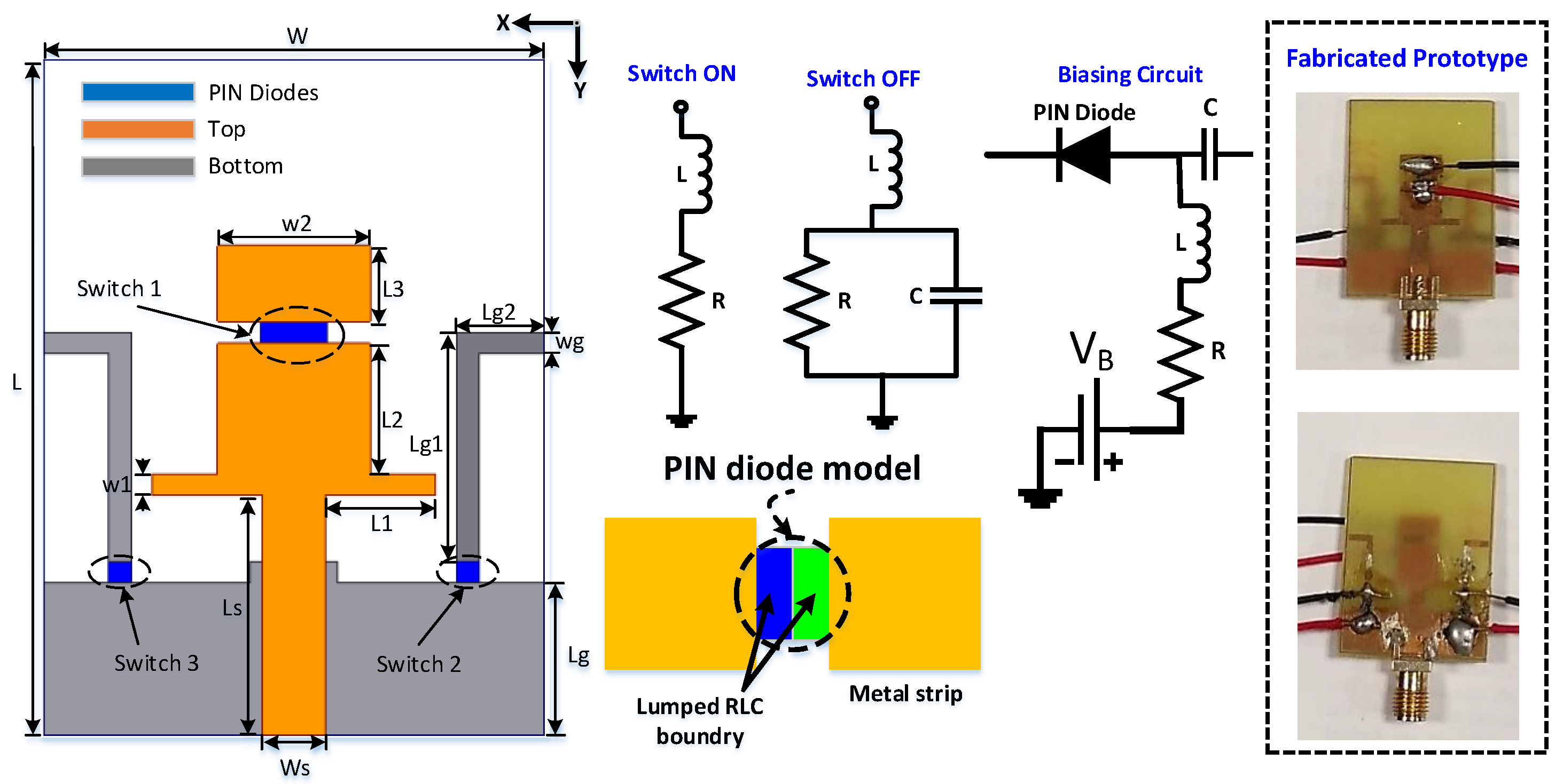
2.1. Switching Techniques

Usually the PIN diode behaves as a variable resistor in the RF frequency range, however, the ON and OFF states have more complex circuitry. Equivalent circuits of the ON and OFF states of the PIN diode consist of an inductor (L) and resistor (R). Forward biasing for the diode is obtained when the inductor and resistor (R) are connected in series. In case of the OFF state, the inductor is connected with a parallel-connected resistor (R) and capacitor (C). The ON and OFF behavior of the PIN diode are studied as RL and RLC circuits, respectively [28]. The lower value of the R in the RL circuit allows current flow between the radiating parts. The higher value of RC in the RLC circuit blocks the current from flowing between the radiating elements. Thus for the sake of simplicity we modeled our PIN diode as an RL circuit in the simulation. The value of the inductor (L) is kept constant. A resistor (R) value is kept low as 1 Ω for ON state of the diode and high as 5 M Ω for OFF state of the diode. A biasing voltage ( V B ) of 3 V and 0 V is applied to the circuitry for switch ON and switch OFF condition, respectively.

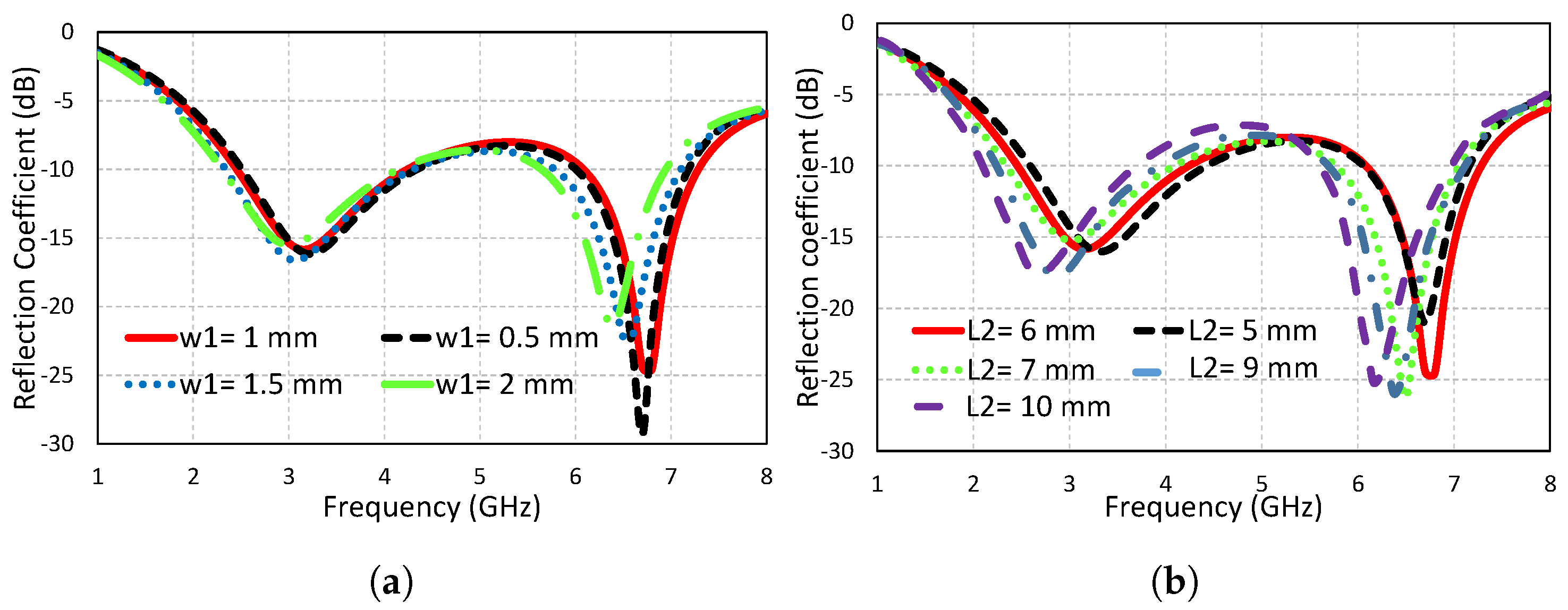
2.2. Antenna’s Parametric Analysis

High Frequency Structure Simulator (HFSS 13.0) is used for designing of the proposed antenna. The reflection coefficient (S11) of the designed antenna under ON and OFF states of the switch 1 is illustrated in Figure 3. It is clear from Figure 3 that the proposed antenna has a single frequency band in the OFF state of Switch 1. Dual band antenna performance can be achieved by changing the state of Switch 1 to the ON state, as shown in Figure 3.
Parametric examination of various parameters of the proposed antenna is performed so as to assess the impact of different parameters on the antenna performance. The proposed antenna is assessed using the parameters w1 and L2. It can be seen from the graph of varying parameter w1 that w1 has a large effect on the band centered at 6.8 GHz. Changing the parameter w1 dramatically changes the resonant frequency of the 6.8 GHz band. By increasing the value of the parameter w1, the resonant frequency of the second band shifts towards the lower frequency, whereas the effect on the first resonant band is negligible. Thus, it is concluded from the parametric analysis that the second resonant band can be controlled by the parameter w1. Figure 4a demonstrates the simulated S11 of the proposed antenna versus frequencies for varied w1.
Figure 4b presents the simulated S11 of the proposed antenna versus frequencies for a range of values of the parameter L2. It is clear from the figure that the parameter L2 is effective in shifting of both bands. By increasing the value of L2, both bands shift toward lower frequency. From [27], it is clear that the frequency is inversely related to length of the monopole. The physical length of the radiating element increases, which corresponds to a lower operating frequency (1).

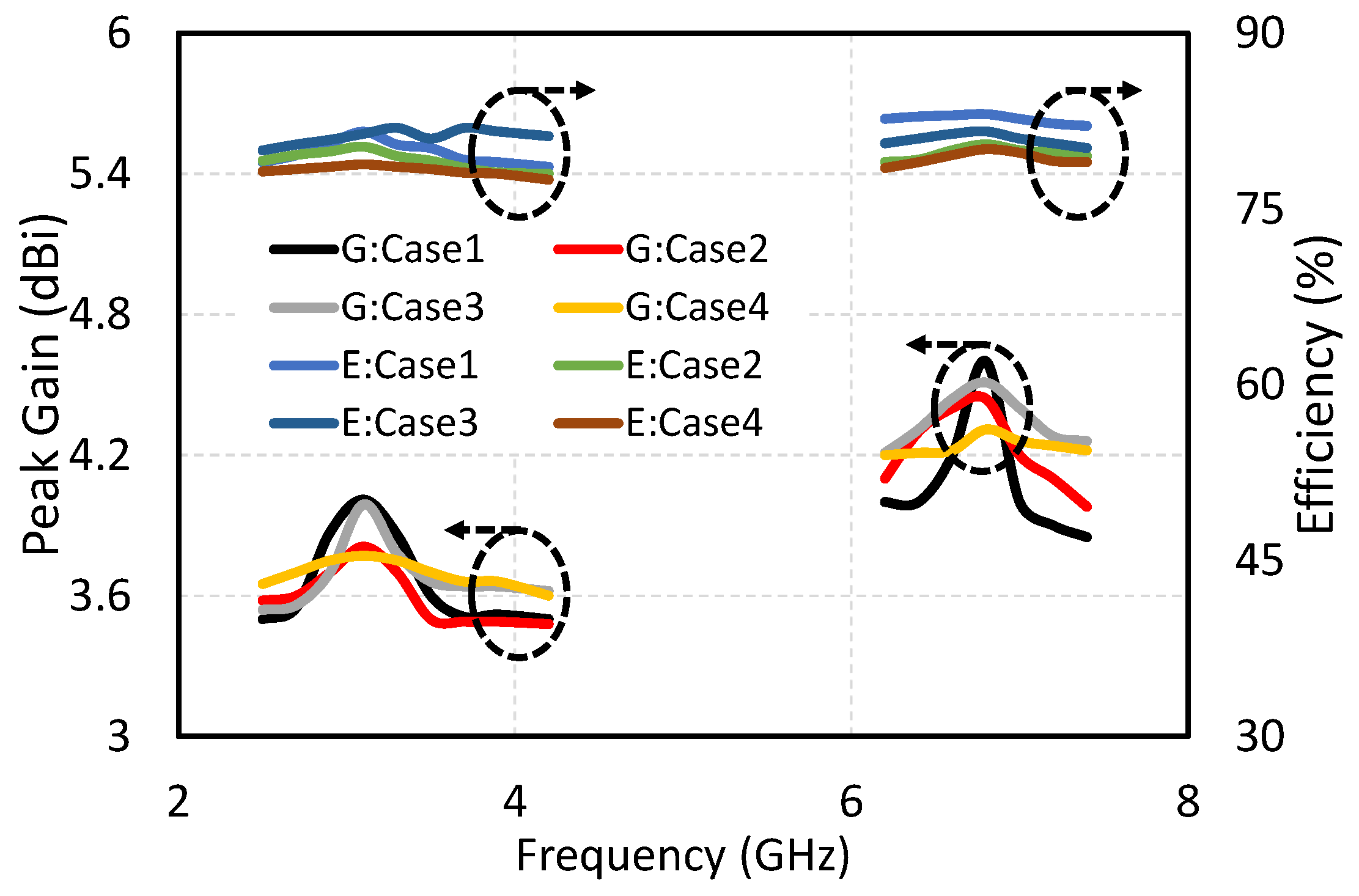
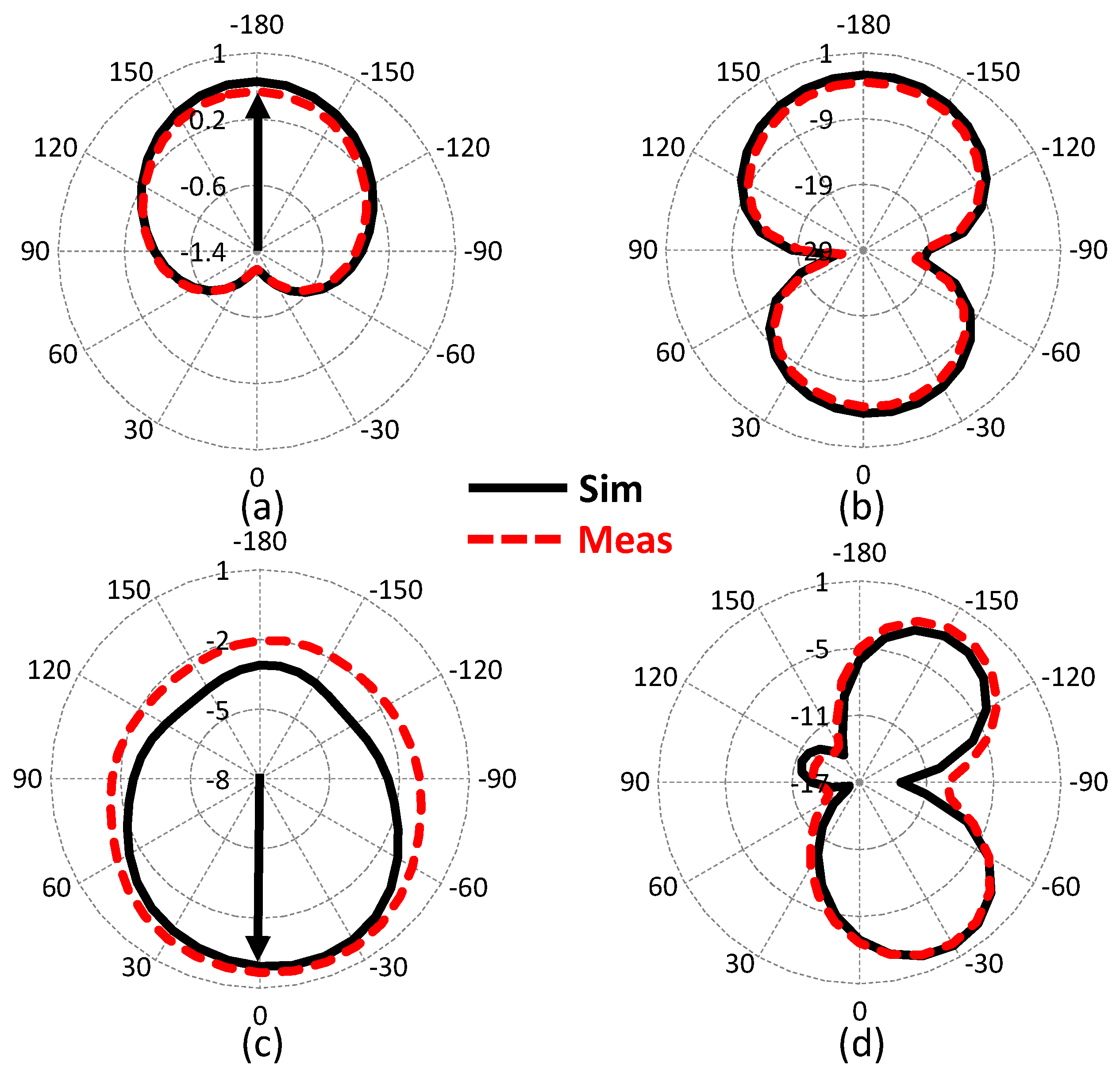
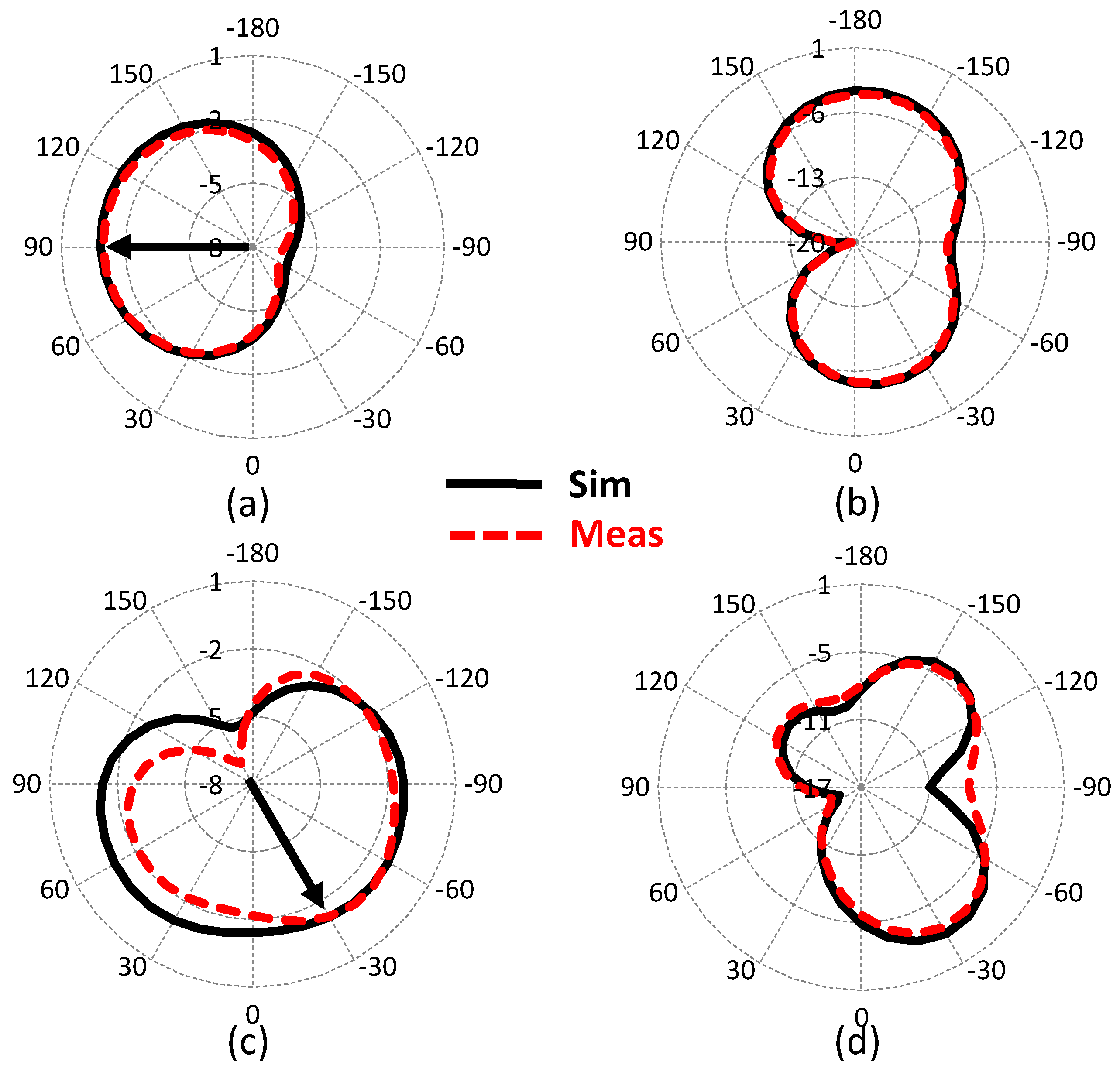
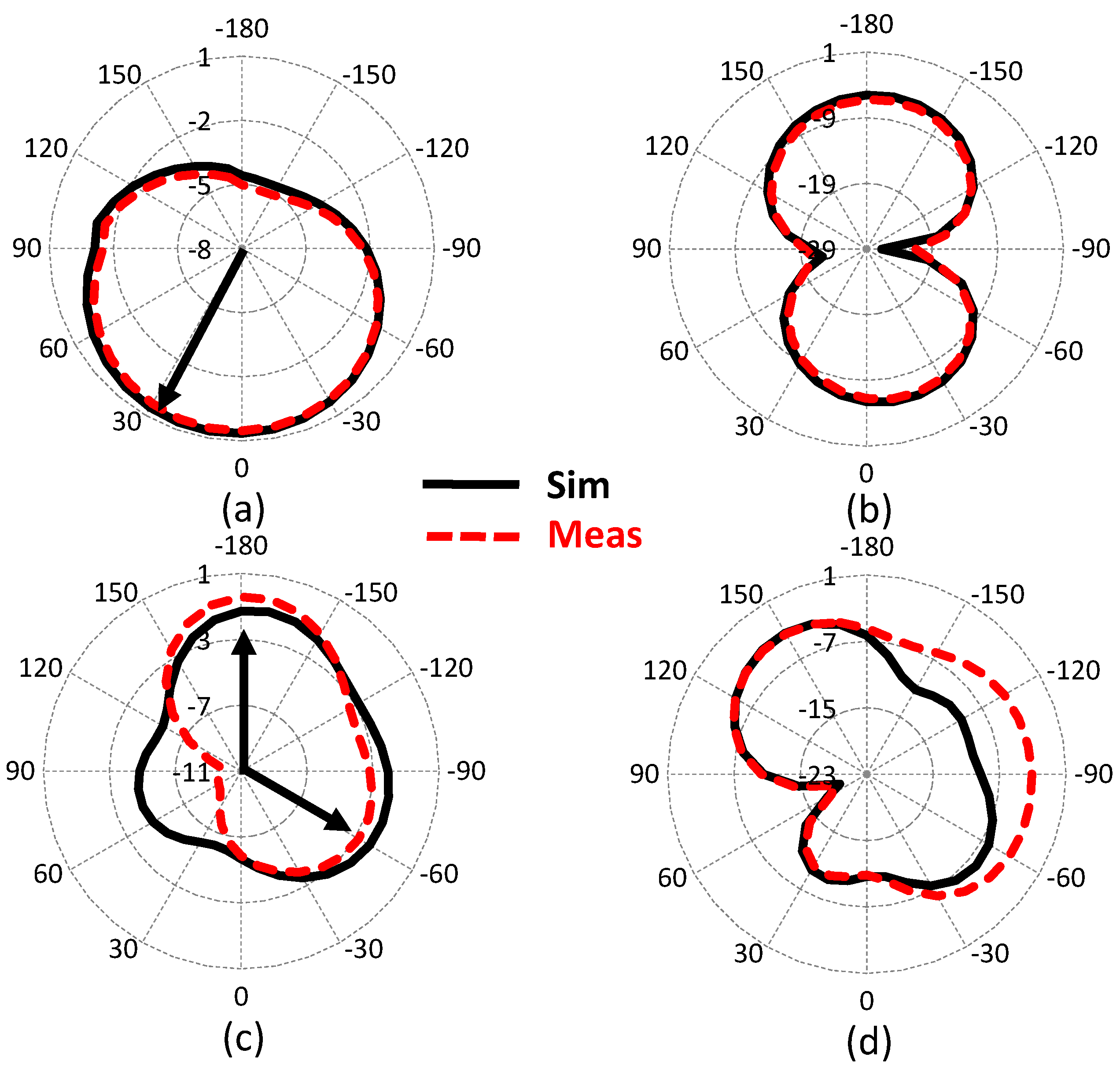
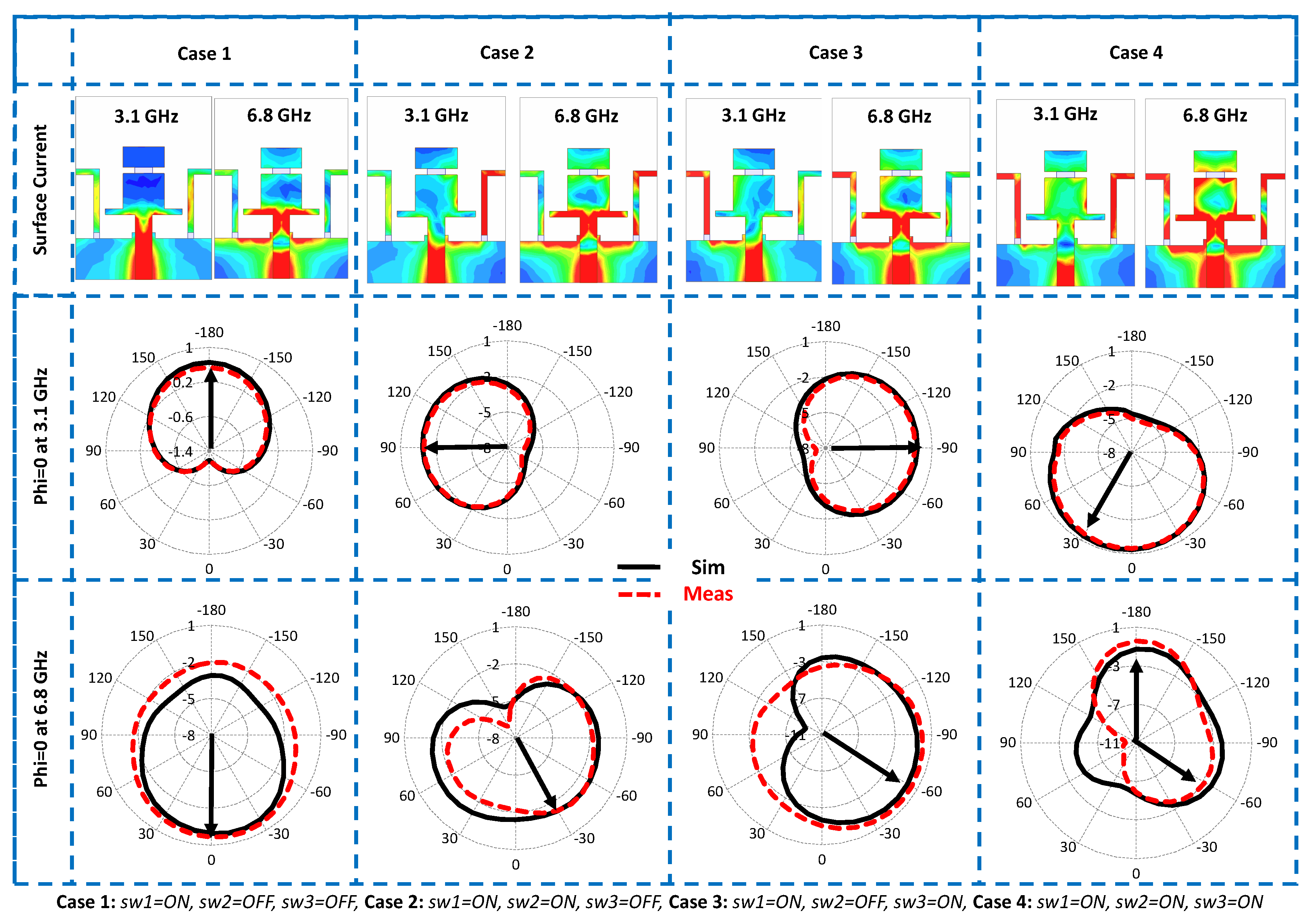
3. Results and Discussions

Figure 1 shows the top and bottom of the fabricated antenna. A low-capacitance PIN diode, MPP4203 (Microsemi) is used in the fabricated antenna. The DC path is completely isolated from the feeding path. The capacitors have the ability to block DC and pass RF signals while the RF choke (RFC) blocks RF and passes DC. The fabricated antenna uses 125 nH inductors, and 470 pF capacitors. The fabricated prototype is measured for reflection coefficient, and gain using Agilent Vector Network Analyzer (VNA). The calibration of the VNA is performed using SOLT (short-open-load-through) technique. After calibrating the VNA, fabricated prototype is connected with VNA and reflection coefficient is obtained. A 6dB log periodic antenna is placed at a distance of 8 m from the proposed antenna for far field pattern measurements. The fabricated antenna is placed on turn-table and the motor is allowed to rotate the antenna with 10 steps in both principle planes.
The proposed antenna has a resonant frequency of 3.1 GHz covering a 10 dB bandwidth of 1.7 GHz, as shown in Figure 5, when the lumped switch (Switch 1) is OFF. The antenna covers two bands when the lumped switch (Switch 1) is ON. The antenna has resonant frequencies of 3.1 GHz and 6.8 GHz, covering 10 dB bandwidths of 1.7 GHz and 1.2 GHz, respectively, when the lumped switch of the proposed antenna is ON.
Figure 5 compares the simulated and measured reflection coefficient (S11) results in both ON and OFF state of the switch (Switch 1). The simulated and measured results are well-matched. The slight mismatch in the curves for S11 is caused by the introduction of the three lumped switches in the fabricated antenna, SMA connector losses and cable losses.
To further characterize the behavior of the proposed antenna, the surface current distributions at 3.1 GHz and 6.8 GHz are shown in Figure 6. It is clear from Figure 6 that the current density is higher at the lower side of the radiating part with respect to the remaining portion of the radiator for 3.1 GHz. It is clear from Figure 6 that the lower region is responsible for resonance at 3.1 GHz. The surface current density of the proposed antenna is higher at lower as well as upper portions of the antenna at 6.8 GHz indicating that the 6.8 GHz resonance is affected by lower as well as upper parts of the antenna. The simulated gain and efficiency of the antenna under all switching cases is illustrated in Figure 7.
Figure 8, Figure 9, Figure 10 and Figure 11 present the radiation patterns for Case 1, Case 2, Case 3, and Case 4, respectively. The radiation patterns for both Phi = 0 and Phi = 90 are simulated and measured. Figures for all cases compare the simulated and measured radiation patterns of the proposed antenna at 3.1 and 6.8 GHz. Due to time varying current on the ground plane, size and structure of the ground plane is important factor in determining the impedance and radiation properties of the antenna. The introduction of L-shaped stub on the ground has very little impact on the impedance, however a huge impact on the radiation of the antenna is observed. Unique current distribution is observed in case of all switching condition which leads to different beam tilting phenomenon (Figure 12).
Figure 8 shows the radiation pattern for Case 1 where Switch 1 is ON and the rest of the switches are OFF. It can be seen from Figure 8 that the main lobe at Phi = 0 is directed towards 180 while a low backward lobe is observed as compared to the main lobe at 3.1 GHz. In the Phi = 0 plane, the main lobe is directed towards 0 and a low backward lobe is observed at 6.8 GHz. At lower frequency band the designed antenna radiates predominantly as a “Figure of Eight” in Phi = 90 plane while a little distortion is observed at high frequency band.
Figure 9 shows the radiation pattern for Case 2 where Switch 1 and Switch 2 are ON, and Switch 3 is OFF. In this case, the current flows along the L-shaped stub connected with ground plane as shown in Figure 12. The major current contents are present on the right sided L-shaped stub, resulting in enhancing the beam in one direction (90 at 3.1 GHz and −30 at 6.8 GHz) while suppressing the beam in opposite direction. It is quite clear from Figure 9 that the main lobe of the proposed antenna is directed towards 90 for Phi = 0 at 3.1 GHz, while the main lobe is directed towards −30 for 6.8 GHz. At lower frequency band the designed antenna radiates predominantly as a distorted “Figure of Eight” in Phi = 90 plane, while much more distortion is observed at high frequency band.
Figure 10 shows the radiation pattern for Case 3 where Switch 1 and Switch 3 are ON, and Switch 2 is OFF. Most of the current on the ground plane is concentrated on left sided L-shaped stub (Figure 12) which act as a director and tilt the beam towards −90 at 3.1 GHz and −60 at 6.8 GHz. It is clear from Figure 10 that the main lobe of the proposed antenna is directed towards 270 for Phi = 0 at 3.1 GHz while main lobe is directed towards −60 at 6.8 GHz.
Figure 11 shows the radiation pattern for Case 4 when Switch 1 and Switch 2 and Switch 3 are ON. Current in the ground plane is concentrated on both L-shaped stubs which results in suppressing the power in the opposite direction (resulting in directing beam at 30 for 3.1 GHz and −60 /180 for 6.8 GHz). It is clear from Figure 11 that the main lobe of the proposed antenna is directed towards 30 for Phi = 0 at 3.1 GHz, while the main lobe is directed towards −60 and 180 at 6.8 GHz. The proposed antenna exhibits stable radiation pattern in all four cases. Also, front-to-back-ratios (FBR) are satisfactory in the directed beams.
Table 2 summarizes the pattern reconfigurability of the proposed antenna achieved by adjusting different switching states. Table 3 compares the simulated gain, measured gain and simulated efficiency of the antenna for four possible cases. It can be concluded from the Table 3 that the antenna has good simulated and measured gain and satisfactory simulated efficiency at four possible cases. Table 4 compares the proposed antenna with the antennas reported in the literature. The proposed antenna novelty lies in its simple shape and its ability to efficiently reconfigure the frequency and beam direction. It can be well noted that the proposed antenna has smaller dimensions than the antennas reported in the literature. Also, the proposed antenna uses minimum number of switches which in turn reduces the losses occurred by the switches and also reduce the complexity level of the design. The antenna presented in this work has wider bandwidth than the existing antennas along with higher peak gain.

4. Conclusions

A compact printed antenna having the functionality of frequency shifting as well as pattern reconfigurability is successfully designed and experimentally validated in this paper. The proposed antenna is switch-dependent and has dissimilar performance for ON and OFF states of Switch 1. The designed antenna can be operated at two unique frequencies, depending on the state of Switch 1. When Switch 1 is OFF, the antenna operates at 3.1 GHz. Changing the state of Switch 1 causes the antenna to operate at 3.1 GHz (UWB health monitoring band for pets) and 6.8 GHz (indoor UWB band) with good gain (4.01 dBi and 4.6 dBi, respectively). The pattern reconfigurability is obtained by changing the states of Switch 2 and Switch 3 introduced in the ground plane. Four different beam directions may be obtained by adjusting the states of Switch 2 and Switch 3 while the maintaining high gain and efficiency.

Author Contributions

A.I. and A.S. provided the idea, performed the experiments, and managed the paper. N.K.M., R.G., I.E., J.R., and S.K. assisted in the idea development and paper writing.

Funding

This research was supported by the Research Program through the National Research Foundation of Korea (NRF-2016R1D1A1B03934653, NRF-2019R1A2C1005920). The authors also extend their appreciation to the Deanship of Scientific Research at Majmaah University for supporting this work through research project No.1440-80.

Conflicts of Interest

The authors declare no conflict of interest.

References

  1. Augustin, G.; Aanandan, C.; Mohanan, P.; Vasudevan, K. A reconfigurable dual-frequency slot-loaded microstrip antenna controlled by pin diodes. Microw. Opt. Technol. Lett. 2005, 44, 374–376. [Google Scholar]
  2. Ojaroudi Parchin, N.; Jahanbakhsh Basherlou, H.; Al-Yasir, Y.I.; Abd-Alhameed, R.A.; Abdulkhaleq, A.M.; Noras, J.M. Recent Developments of Reconfigurable Antennas for Current and Future Wireless Communication Systems. Electronics 2019, 8, 128. [Google Scholar] [CrossRef]
  3. Tang, H.; Chen, J.X. Microfluidically frequency-reconfigurable microstrip patch antenna and array. IEEE Access 2017, 5, 20470–20476. [Google Scholar] [CrossRef]
  4. Tang, M.C.; Wen, Z.; Wang, H.; Li, M.; Ziolkowski, R.W. Compact, Frequency-Reconfigurable Filtenna with Sharply Defined Wideband and Continuously Tunable Narrowband States. IEEE Trans. Antennas Propag. 2017, 65, 5026–5034. [Google Scholar] [CrossRef]
  5. Abdulraheem, Y.I.; Oguntala, G.A.; Abdullah, A.S.; Mohammed, H.J.; Ali, R.A.; Abd-Alhameed, R.A.; Noras, J.M. Design of frequency reconfigurable multiband compact antenna using two PIN diodes for WLAN/WiMAX applications. IET Microw. Antennas Propag. 2017, 11, 1098–1105. [Google Scholar] [CrossRef]
  6. Rouissi, I.; Floc’h, J.M.; Rmili, H.; Trabelsi, H. Design of a frequency reconfigurable patch antenna using capacitive loading and varactor diode. In Proceedings of the 2015 9th European Conference on Antennas and Propagation (EuCAP), Lisbon, Portugal, 13–17 April 2015; pp. 1–4. [Google Scholar]
  7. Sharma, N.; Yadav, M.; Kumar, A. Design of quad-band microstrip-fed stubs-loaded frequency reconfigurable antenna for multiband operation. In Proceedings of the 2017 4th International Conference on Signal Processing and Integrated Networks (SPIN), Noida, India, 2–3 February 2017; pp. 275–279. [Google Scholar]
  8. Iqbal, A.; Ullah, S.; Naeem, U.; Basir, A.; Ali, U. Design, fabrication and measurement of a compact, frequency reconfigurable, modified T-shape planar antenna for portable applications. J. Electr. Eng. Technol. 2017, 12, 1611–1618. [Google Scholar]
  9. Iqbal, A.; Saraereh, O.A. A Compact Frequency Reconfigurable Monopole Antenna for Wi-Fi/WLAN Applications. Prog. Electromagn. Res. 2017, 68, 79–84. [Google Scholar]
  10. Li, H.; Xiong, J.; Yu, Y.; He, S. A simple compact reconfigurable slot antenna with a very wide tuning range. IEEE Trans. Antennas Propag. 2010, 58, 3725–3728. [Google Scholar] [CrossRef]
  11. Hamid, M.R.; Gardner, P.; Hall, P.S.; Ghanem, F. Reconfigurable vivaldi antenna. Microw. Opt. Technol. Lett. 2010, 52, 785–787. [Google Scholar] [CrossRef]
  12. Deo, P.; Mehta, A.; Mirshekar-Syahkal, D.; Nakano, H. An HIS-based spiral antenna for pattern reconfigurable applications. IEEE Antennas Wirel. Propag. Lett. 2009, 8, 196–199. [Google Scholar] [CrossRef]
  13. Kang, W.; Lee, S.; Kim, K. Design of symmetric beam pattern reconfigurable antenna. Electron. Lett. 2010, 46, 1536–1537. [Google Scholar] [CrossRef]
  14. Zhang, S.; Huff, G.; Feng, J.; Bernhard, J. A pattern reconfigurable microstrip parasitic array. IEEE Trans. Antennas Propag. 2004, 52, 2773–2776. [Google Scholar] [CrossRef]
  15. Cai, X.; Wang, A.; Chen, W. A circular disc-shaped antenna with frequency and pattern reconfigurable characteristics. In Proceedings of the 2011 China-Japan Joint Microwave Conference Proceedings (CJMW), Hangzhou, China, 20–22 April 2011; pp. 1–4. [Google Scholar]
  16. Chen, X.; Zhao, Y. Dual-band Polarization and Frequency Reconfigurable Antenna Using Double Layer Metasurface. AEU-Int. J. Electron. Commun. 2018, 95, 82–87. [Google Scholar] [CrossRef]
  17. Nguyen-Trong, N.; Hall, L.; Fumeaux, C. A dual-band dual-pattern frequency-reconfigurable antenna. Microw. Opt. Technol. Lett. 2017, 59, 2710–2715. [Google Scholar] [CrossRef]
  18. Majid, H.A.; Rahim, M.K.A.; Hamid, M.R.; Ismail, M.F. Frequency and Pattern Reconfigurable Slot Antenna. IEEE Trans. Antennas Propag. 2014, 62, 5339–5343. [Google Scholar] [CrossRef]
  19. Li, P.K.; Shao, Z.H.; Wang, Q.; Cheng, Y.J. Frequency and Pattern Reconfigurable Antenna for Multi-Standard Wireless Applications. Group 2015, 1, D3. [Google Scholar]
  20. Nikolaou, S.; Bairavasubramanian, R.; Lugo, C.; Carrasquillo, I.; Thompson, D.C.; Ponchak, G.E.; Papapolymerou, J.; Tentzeris, M.M. Pattern and frequency reconfigurable annular slot antenna using PIN diodes. IEEE Trans. Antennas Propag. 2006, 54, 439–448. [Google Scholar] [CrossRef]
  21. Zhao, Y.; Huang, C.; Qing, A.; Luo, X. A Frequency and Pattern Reconfigurable Antenna Array Based on Liquid Crystal Technology. IEEE Photonics J. 2017, 9, 1–7. [Google Scholar] [CrossRef]
  22. Selvam, Y.P.; Kanagasabai, M.; Alsath, M.G.N.; Velan, S.; Kingsly, S.; Subbaraj, S.; Rao, Y.V.R.; Srinivasan, R.; Varadhan, A.K.; Karuppiah, M. A Low-Profile Frequency- and Pattern-Reconfigurable Antenna. IEEE Antennas Wirel. Propag. Lett. 2017, 16, 3047–3050. [Google Scholar] [CrossRef]
  23. Zhu, Z.; Wang, P.; You, S.; Gao, P. A Flexible Frequency and Pattern Reconfigurable Antenna for Wireless Systems. Prog. Electromagn. Res. 2018, 76, 63–70. [Google Scholar]
  24. Zainarry, S.N.M.; Nguyen-Trong, N.; Fumeaux, C. A Frequency-and Pattern-Reconfigurable Two-Element Array Antenna. IEEE Antennas Wirel. Propag. Lett. 2018, 17, 617–620. [Google Scholar] [CrossRef]
  25. Dewan, R.; Abd Rahim, M.K.; Hamid, M.R.; Himdi, M.; Majid, H.B.A.; Samsuri, N.A. HIS-EBG Unit Cells for Pattern and Frequency Reconfigurable Dual Band Array Antenna. Prog. Electromagn. Res. 2018, 76, 123–132. [Google Scholar] [CrossRef]
  26. Han, L.; Wang, C.; Zhang, W.; Ma, R.; Zeng, Q. Design of Frequency-and Pattern-Reconfigurable Wideband Slot Antenna. Int. J. Antennas Propag. 2018, 2018. [Google Scholar] [CrossRef]
  27. Stutzman, W.L.; Thiele, G.A. Antenna Theory and Design; John Wiley & Sons: Hoboken, NJ, USA, 2013. [Google Scholar]
  28. Yeom, I.; Choi, J.; Kwoun, S.s.; Lee, B.; Jung, C. Analysis of RF front-end performance of reconfigurable antennas with RF switches in the far field. Int. J. Antennas Propag. 2014, 2014, 385730. [Google Scholar] [CrossRef]
Figure 1. Proposed antenna diagram, biasing circuit for PIN diode and Fabricated antenna.
Electronics 08 00407 g001
Figure 2. Reflection coefficient analysis for all cases with (a) I-shaped stub, (b) H-shaped stub, (c) L-shaped stub.
Electronics 08 00407 g002
Figure 3. Reflection coefficient of the proposed antenna at ON and OFF switch.
Electronics 08 00407 g003
Figure 4. Reflection coefficient against frequencies for varied parameter (a) w1 (b) L2.
Electronics 08 00407 g004
Figure 5. Simulated and measured reflection coefficient of the proposed antenna.
Electronics 08 00407 g005
Figure 6. Surface current density of the proposed antenna at ON switch condition.
Electronics 08 00407 g006
Figure 7. Simulated peak gains and efficiencies for all switching cases (G = Peak gain and E = efficiency).
Electronics 08 00407 g007
Figure 8. Case 1: (a) Phi = 0 at 3.1 GHz (b) Phi = 90 at 3.1 GHz (c) Phi = 0 at 6.8 GHz (d) Phi = 90 at 6.8 GHz.
Electronics 08 00407 g008
Figure 9. Case 2: (a) Phi = 0 at 3.1 GHz (b) Phi = 90 at 3.1 GHz (c) Phi = 0 at 6.8 GHz (d) Phi = 90 at 6.8 GHz.
Electronics 08 00407 g009
Figure 10. Case 3: (a) Phi = 0 at 3.1 GHz (b) Phi = 90 at 3.1 GHz (c) Phi = 0 at 6.8 GHz (d) Phi = 90 at 6.8 GHz.
Electronics 08 00407 g010
Figure 11. Case 4: (a) Phi = 0 at 3.1 GHz (b) Phi = 90 at 3.1 GHz (c) Phi = 0 at 6.8 GHz (d) Phi = 90 at 6.8 GHz.
Electronics 08 00407 g011
Figure 12. Summary of the beam switching using switch 2 and switch 3.
Electronics 08 00407 g012
Table 1. Different Parameter and values of the antenna.
ParameterValue (mm)ParameterValue (mm)ParameterValue (mm)
W23L15.05Lg24
L31L26Lg110.5
L33.5W11Wg1
W27Ws3Lg7
Ls9.5
Table 2. Summary of the state of switches and corresponding main lobe direction.
CaseSwitch 1Switch 2Switch 3Main Lobe Direction at Phi = 0 for 3.1 GHzMain Lobe Direction at Phi = 0 for 6.8 GHz
1ONOFFOFF180 0
2ONONOFF90 −30
3ONOFFON−90 −60
4ONONON30 −60 and 180
Table 3. Summary of the different cases and its corresponding gains and efficiencies at both bands.
CaseGain (dBi)Efficiency (%)Gain (dBi)Efficiency (%)
Sim (3.1 GHz)Meas (3.1 GHz)Sim (6.8 GHz)Meas (6.8 GHz)
14.013.9381.64.604.5883.1
23.813.7880.34.444.3580.5
33.993.8981.44.514.4681.6
43.773.7078.84.314.2180.1
Table 4. Performance comparison with previously published work.
Ref.Size (mm 2 )ReconfigurationActuatorsBandwidth (MHz)Peak Gain (dBi)
 [18]130 × 160Frequency and Pattern11 PIN diodes200/150/1505.6/4.6/3.3
[19]80 × 45.8Frequency and Pattern5 PIN diodes580/2902.1/4.8
[20]50 × 50Frequency and Pattern2 PIN diodes100/704/5.6
[22]50 × 50Frequency and Pattern4 PIN diodes180/200/180/2004/3.8/4.4/5
[23]42 × 44Frequency and Pattern8 PIN diodes160/220NG
[24]160.9 × 151.5Frequency and Pattern2 Varactor diodes2309
[25]70 × 70Frequency and Pattern4 PIN diodesNG0.521/7.833
[26]40 × 30Frequency and Pattern4 PIN diodes400/5002.24–2.76
This Work23 × 31Frequency and Pattern3 PIN diodes1700/12004.01/4.60

