Design of a Wide-Band Voltage-Controlled Ring Oscillator Implemented in 180 nm CMOS Technology

 ,
,  ,
,
Abstract
:1. Introduction
2. VCO-Based on CMOS Differential Stages
2.1. CMOS Differential Stage with Passive Load
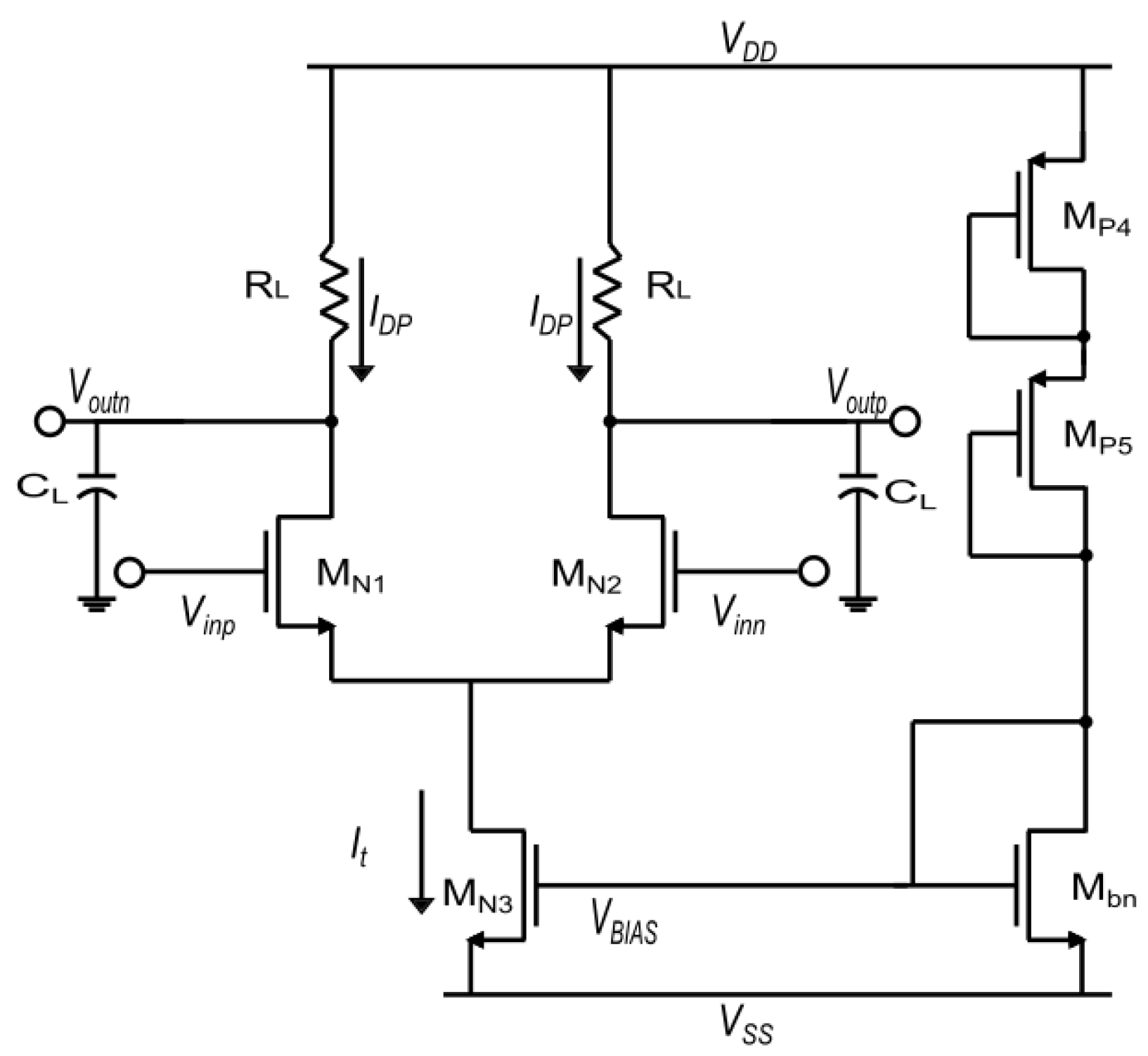
2.2. CMOS Differential Stage with Active Load
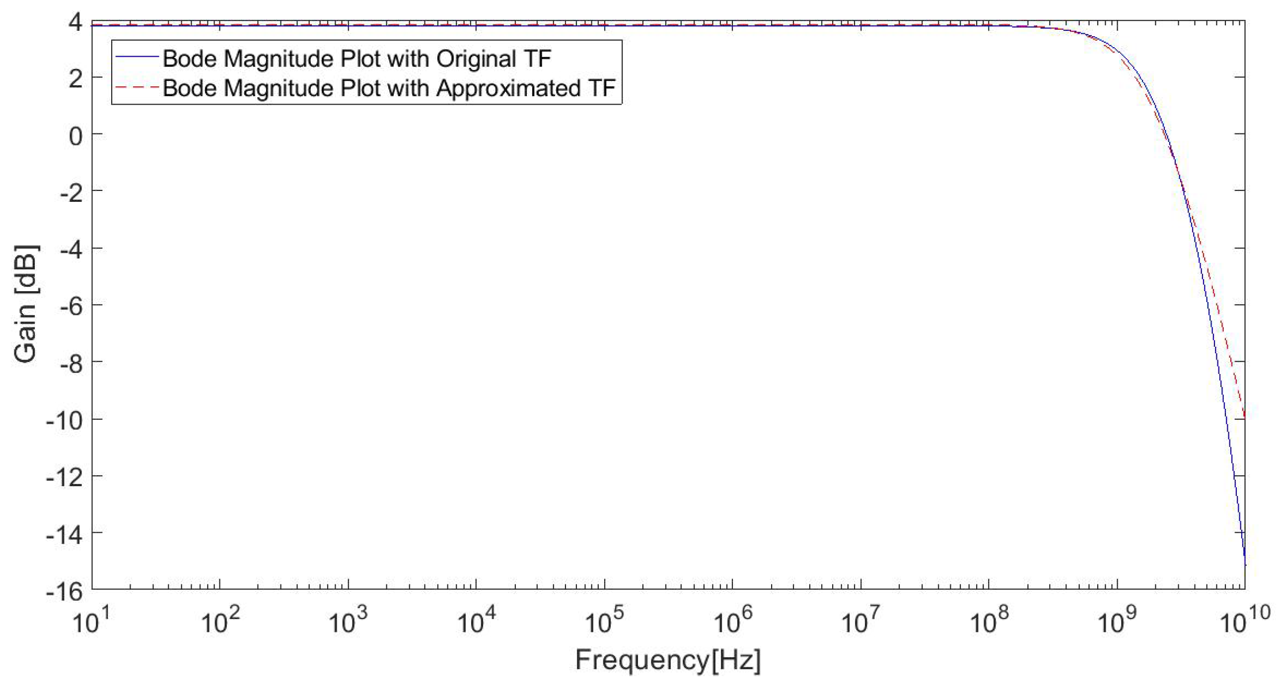
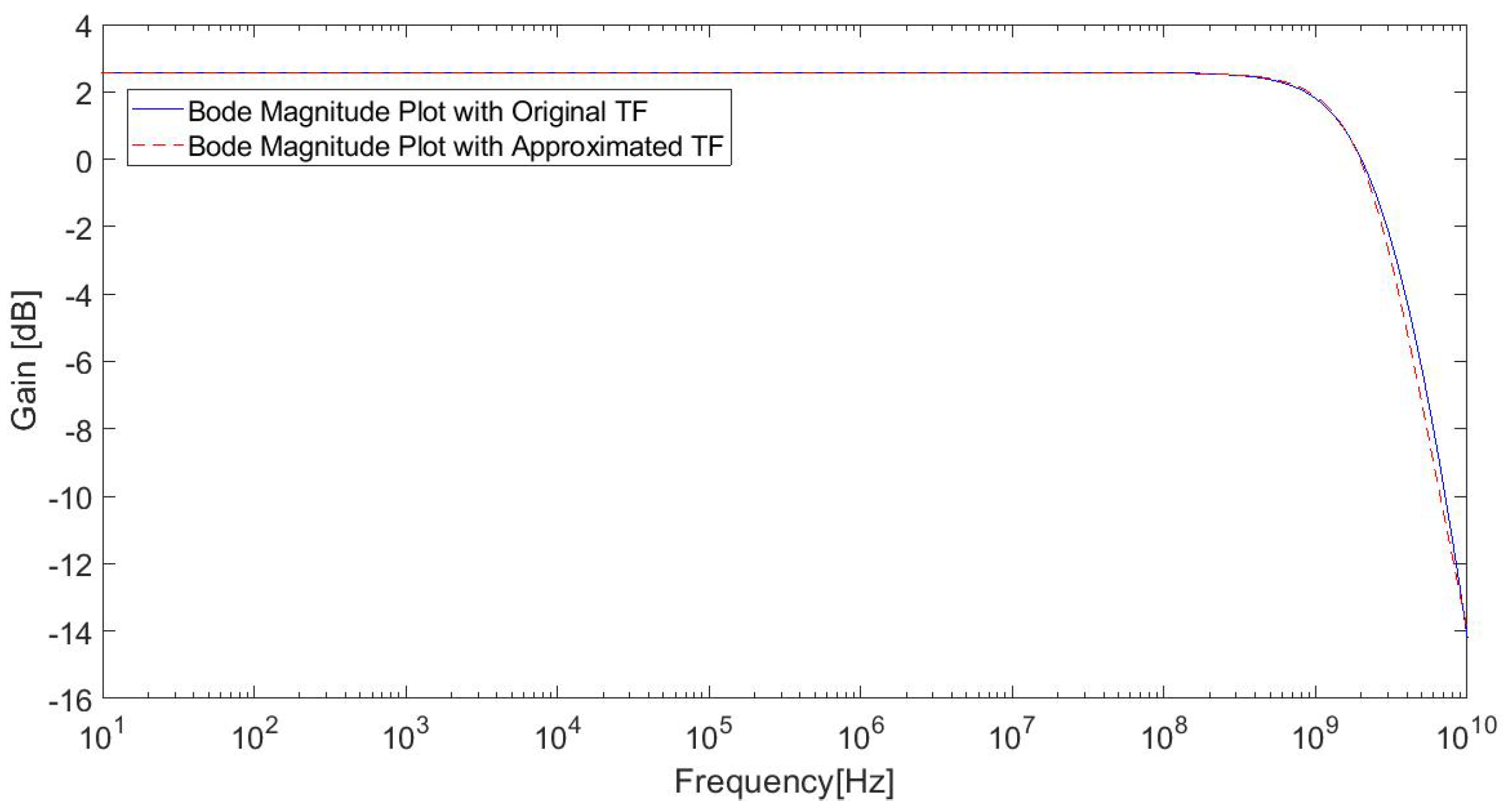
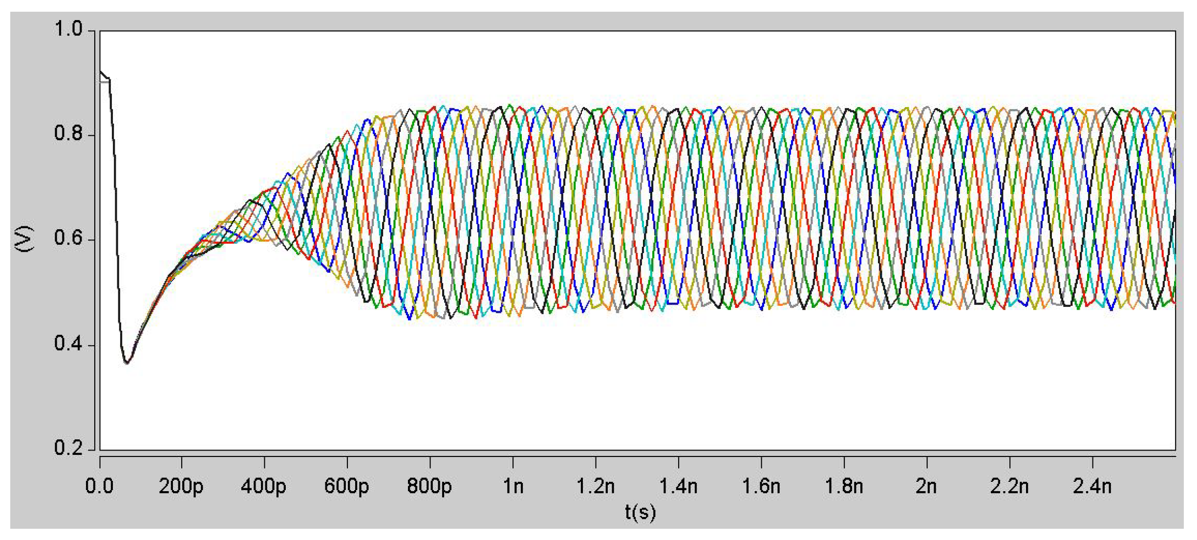
2.3. Voltage Controlled Oscillator Based on CMOS Differential Stages
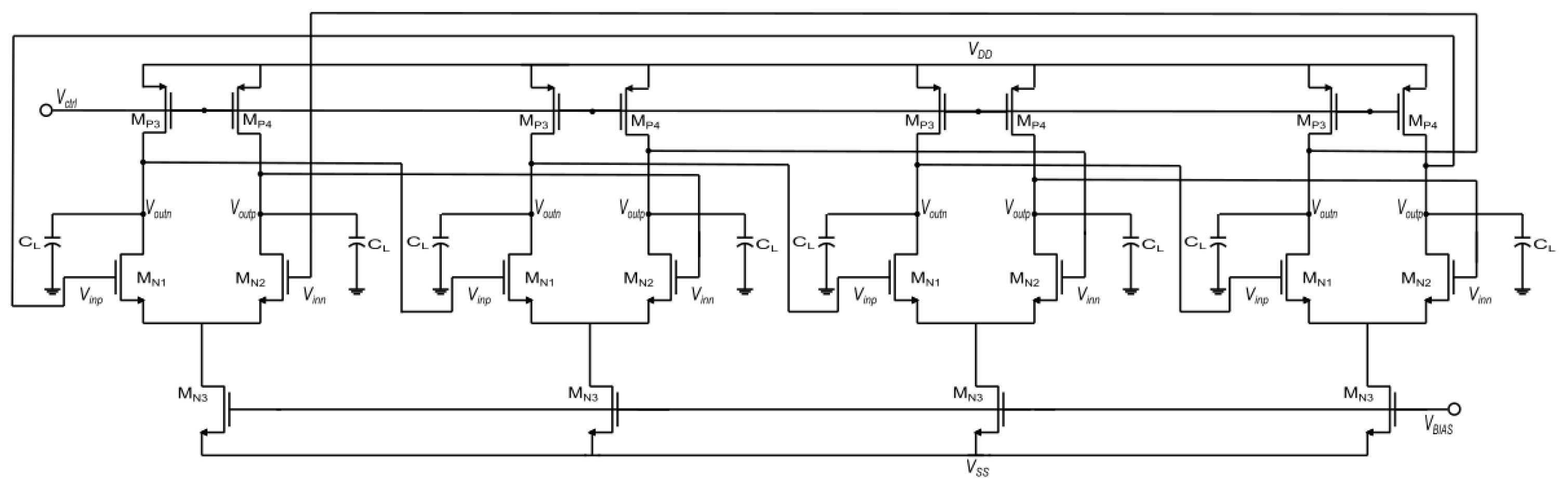
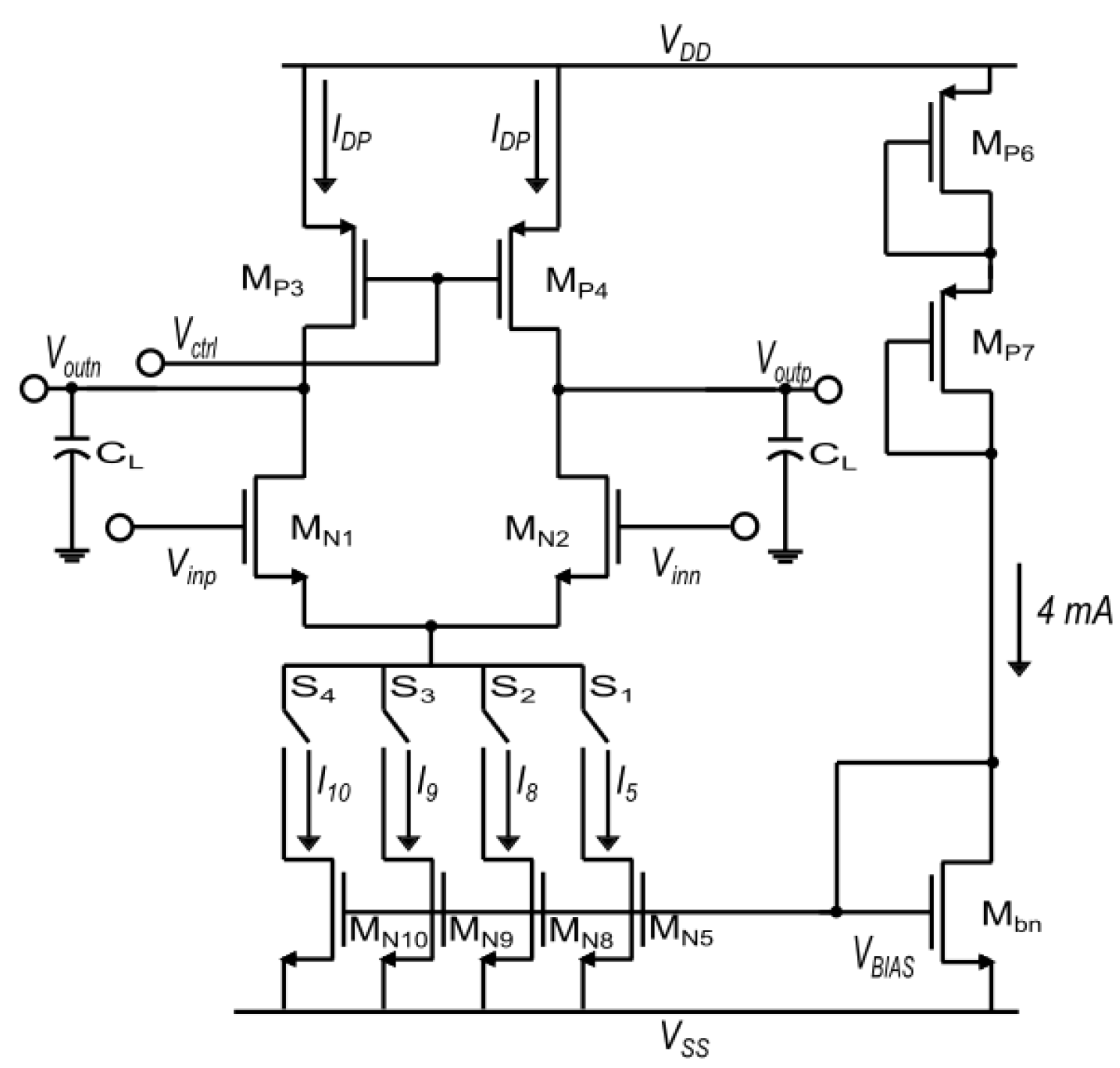
3. VCO with Programmable Tail Currents
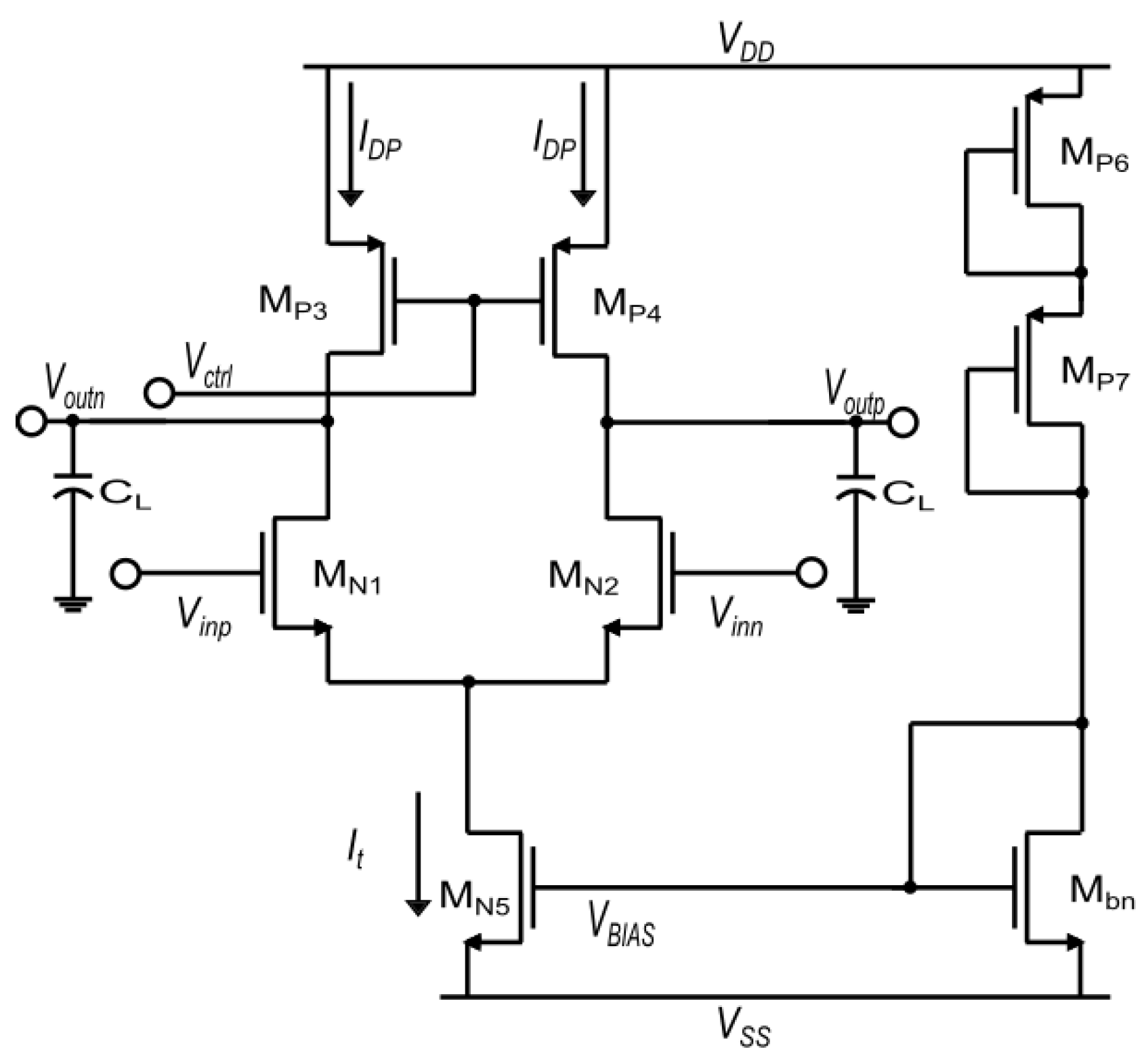
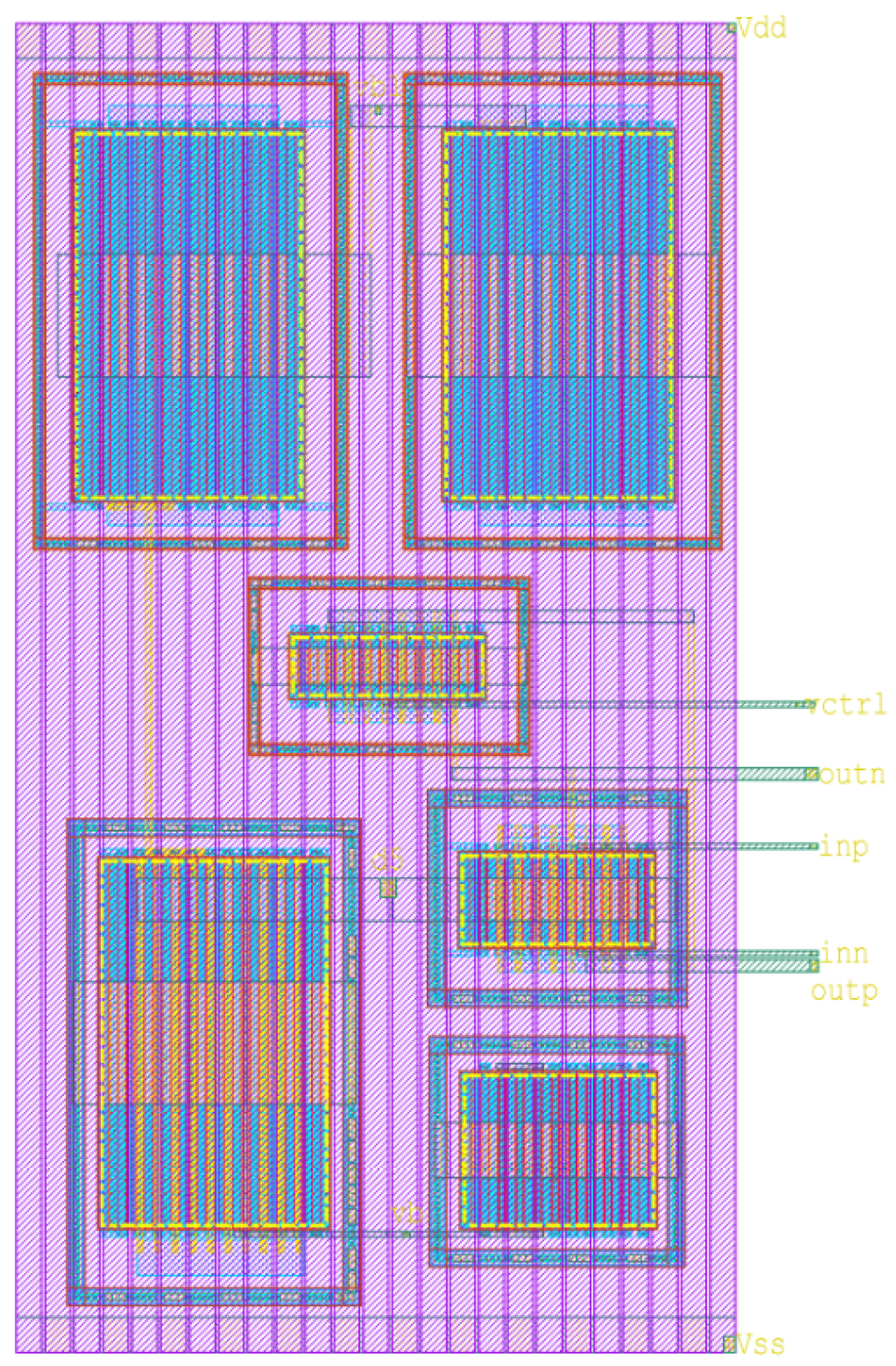
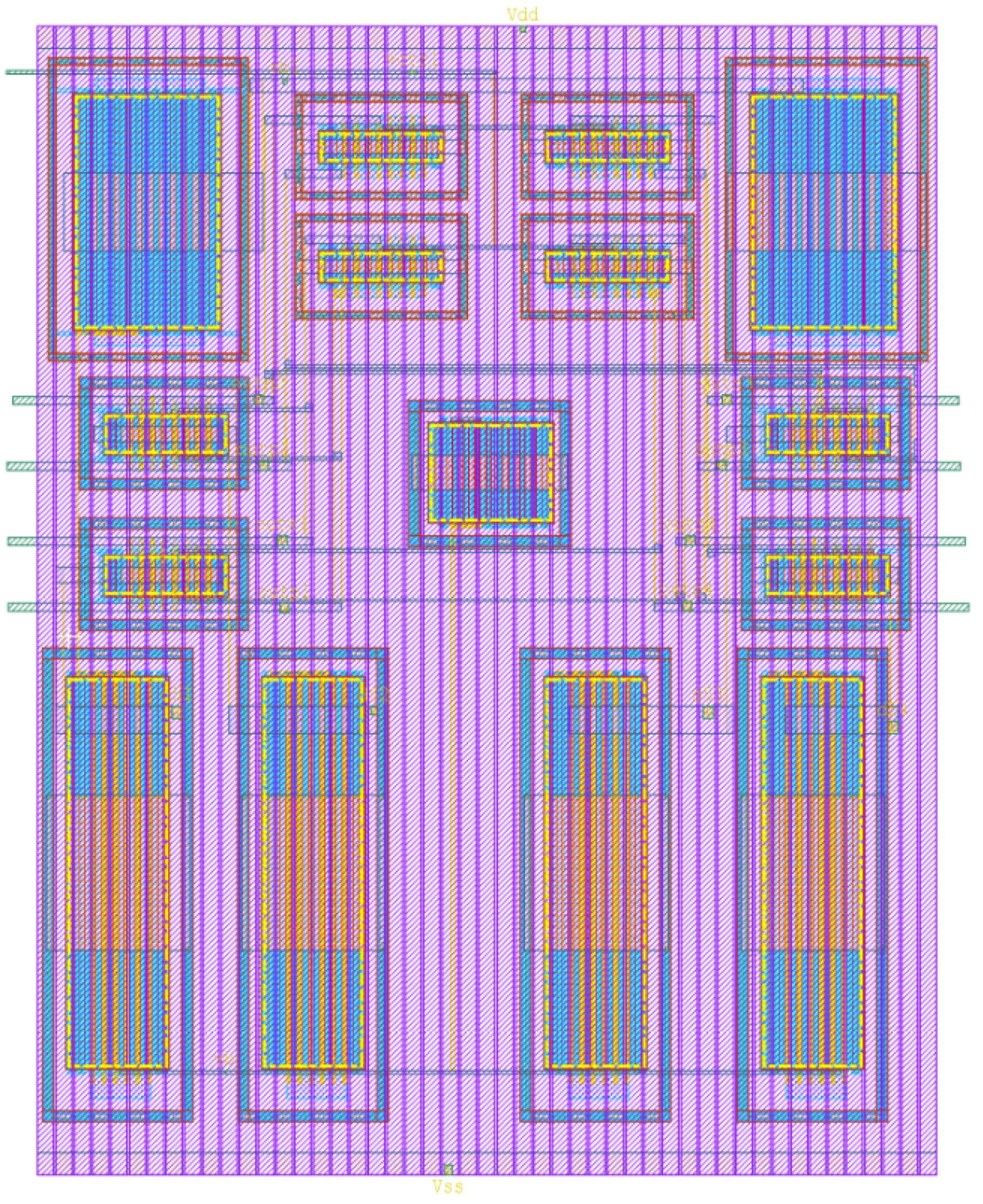
4. Layout Design of the VCO Based on CMOS Differential Stages with Active Load
5. Conclusions
Author Contributions
Funding
Conflicts of Interest
References
- Tanaka, M.; Ozawa, S.; Mori, S. Rewritable programmable logic array of current mode logic. IEEE Trans. Comput. 1981, 30, 229–234. [Google Scholar] [CrossRef]
- Einspruch, N. The VLSI Handbook; CRC Press: Boca Raton, FL, USA, 2012. [Google Scholar]
- Mizuno, M.; Yamashina, M.; Furuta, K.; Igura, H.; Abiko, H.; Okabe, K.; Ono, A.; Yamada, H. A GHz MOS adaptive pipeline technique using MOS current-mode logic. IEEE J. Solid-State Circuits 1996, 31, 784–791. [Google Scholar] [CrossRef]
- Hsieh, J.Y.; Lin, K.Y. A 0.7-mW LC Voltage-Controlled Oscillator Leveraging Switched Biasing Technique for Low Phase Noise. IEEE Trans. Circuits Syst. II Express Briefs 2019, 66, 1307–1310. [Google Scholar] [CrossRef]
- Basaligheh, A.; Saffari, P.; Winkler, W.; Moez, K. A Wide Tuning Range, Low Phase Noise, and Area Efficient Dual-Band Millimeter-Wave CMOS VCO Based on Switching Cores. IEEE Trans. Circuits Syst. I Regul. Pap. 2019, 66, 2888–2897. [Google Scholar] [CrossRef]
- Poor, M.A.; Esmaeeli, O.; Sheikhaei, S. A low phase noise quadrature VCO using superharmonic injection, current reuse, and negative resistance techniques in CMOS technology. Analog Integr. Circuits Signal Process. 2019, 99, 633–644. [Google Scholar] [CrossRef]
- Ghorbel, I.; Haddad, F.; Rahajandraibe, W.; Loulou, M. Design Methodology of Ultra-Low-Power LC-VCOs for IoT Applications. J. Circuits Syst. Comput. 2019, 28. [Google Scholar] [CrossRef]
- Al-Tamimi, K.M.; El-Sankary, K.; Fouzar, Y. VCO-Based ADC With Built-In Supply Noise Immunity Using Injection-Locked Ring Oscillators. IEEE Transa. Circuits Syst. II Express Briefs 2019, 66, 1089–1093. [Google Scholar] [CrossRef]
- Ding, Z.; Zhou, X.; Li, Q. A 0.5-1.1-V Adaptive Bypassing SAR ADC Utilizing the Oscillation-Cycle Information of a VCO-Based Comparator. IEEE J. Solid-State Circuits 2019, 54, 968–977. [Google Scholar] [CrossRef]
- Sharma, J.; Krishnaswamy, H. A 2.4- GHz Reference-Sampling Phase-Locked Loop That Simultaneously Achieves Low-Noise and Low-Spur Performance. IEEE J. Solid-State Circuits 2019, 54, 1407–1424. [Google Scholar] [CrossRef]
- Ulansky, V.; Raza, A.; Oun, H. Electronic Circuit with Controllable Negative Differential Resistance and its Applications. Electronics 2019, 8, 409. [Google Scholar] [CrossRef]
- Sun, I.F.; Yin, J.; Mak, P.I.; Martins, R.P. A Comparative Study of 8-Phase Feedforward-Coupling Ring VCOs. IEEE Trans. Circuits Syst. II Express Briefs 2019, 66, 527–531. [Google Scholar] [CrossRef]
- Abidi, A.A. Phase noise and jitter in CMOS ring oscillators. IEEE J. Solid-State Circuits 2006, 41, 1803–1816. [Google Scholar] [CrossRef]
- Wang, Z.; Bai, X.; Diao, S.; Lin, F. An open loop compensation technique for reducing supply sensitivity of CML ring oscillator. Analog Integr. Circuits Signal Process. 2017, 93, 277–285. [Google Scholar] [CrossRef]
- Gui, X.; Green, M.M. Design of CML ring oscillators with low supply sensitivity. IEEE Trans. Circuits Syst. I Regul. Pap. 2013, 60, 1753–1763. [Google Scholar] [CrossRef]
- Zhang, Z.; Chen, L.; Djahanshahi, H. A SEE Insensitive CML Voltage Controlled Oscillator in 65nm CMOS. In Proceedings of the 2018 IEEE Canadian Conference on Electrical & Computer Engineering (CCECE), Quebec City, QC, Canada, 13–16 May 2018; pp. 1–4. [Google Scholar]
- Kishine, K.; Inaba, H.; Ohtomo, Y.; Nakamura, M.; Koizumi, H.; Nakamura, M. Analysis and design based on small-signal equivalent circuit for a lO- GHz ring VCO with 65-nm CMOS. In Proceedings of the 2013 IEEE 56th International Midwest Symposium on Circuits and Systems (MWSCAS), Columbus, OH, USA, 4–7 August 2013; pp. 904–907. [Google Scholar]
- Heydari, P.; Mohanavelu, R. Design of ultrahigh-speed low-voltage CMOS CML buffers and latches. IEEE Trans. Very Large Scale Integr. (VLSI) Syst. 2004, 12, 1081–1093. [Google Scholar] [CrossRef]
- Kumar, M. Design of Linear Low-Power Voltage-Controlled Oscillator with I-MOS Varactor and Back-Gate Tuning. Circuits Syst. Signal Process. 2018, 37, 3685–3701. [Google Scholar] [CrossRef]
- Razavi, B. Design of Analog CMOS Integrated Circuits; McGraw-Hill: New York, NY, USA, 2002. [Google Scholar]
- Meyer, R.G. Noise, Gain and Bandwidth in Analog Design. In Trade-Offs in Analog Circuit Design; Toumazou, C., Moschytz, G., Eds.; Springer: Boston, MA, USA, 2002; pp. 227–256. [Google Scholar]
- Razavi, B. Fundamentals of Microelectronics; Wiley: Hoboken, NJ, USA, 2008. [Google Scholar]
- Duarte-Villaseñor, M.A.; Tlelo-Cuautle, E.; de la Fraga, L.G.; Sánchez-López, C. Symbolic Analysis and Synthesis of Analog Circuits Using Nullors and Pathological Mirror Elements. In Pathological Elements in Analog Circuit Design; Springer: Manhattan, NY, USA, 2018; pp. 3–30. [Google Scholar]
- Palumbo, G.; Pennisi, S. Feedback Amplifiers: Theory and Design; Springer Science & Business Media: Berlin, Germany, 2002. [Google Scholar]
- Maloberti, F. Analog design for CMOS VLSI Systems; Springer Science & Business Media: Berlin, Germany, 2006; Volume 646. [Google Scholar]
- Chen, P.; Cheng, H.C.; Widodo, A.; Tsai, W.X. A PVT insensitive field programmable gate array time-to-digital converter. In Proceedings of the 2013 IEEE Nordic-Mediterranean Workshop on Time-to-Digital Converters (NoMe TDC), Perugia, Italy, 3 October 2013; pp. 1–4. [Google Scholar]
- Jyotsna, K.; Kumar, P.S.; Madhavi, B. Implementation of 8 Bit Microprocessor Using Current Mode Logic (CML) Approach. In Proceedings of the 2018 3rd International Conference for Convergence in Technology (I2CT), Pune, India, 6–8 April 2018; pp. 1–6. [Google Scholar]
- Sedra, A.S.; Smith, K.C. Microelectronic Circuits; Holt, Rinehart and Oxford University Press: Oxford, UK, 1982. [Google Scholar]
- Mansuri, M.; Yang, C.K. A low-power adaptive bandwidth PLL and clock buffer with supply-noise compensation. IEEE J. Solid-State Circuits 2003, 38, 1804–1812. [Google Scholar] [CrossRef]
- Aryasomayajula, L.J.; Khatua, P.; Mal, A.K. Analog-to-digital converter using CML based Ring oscillator with tuning range 1–7.2 GHz in 90 nm CMOS. In Proceedings of the IEEE International Conference on Computer Communication and Systems ICCCS14, Chennai, India, 20–21 February 2014; pp. 130–135. [Google Scholar]
- Chen, H.J.; Jou, J.J.; Shih, T.T. Design of pseudo-random bit sequence generator with adjustable sinusoidal jitter. In Proceedings of the 2016 International SoC Design Conference (ISOCC), Jeju, South Korea, 23–26 October 2016; pp. 263–264. [Google Scholar]
- Mondal, A.J.; Majudmer, A.; Bhattacharyya, B.K. A Design Methodology for MOS Current Mode Logic VCO. In Proceedings of the 2017 IEEE International Symposium on Nanoelectronic and Information Systems (iNIS), Bhopal, India, 18–20 December 2017; pp. 206–209. [Google Scholar]


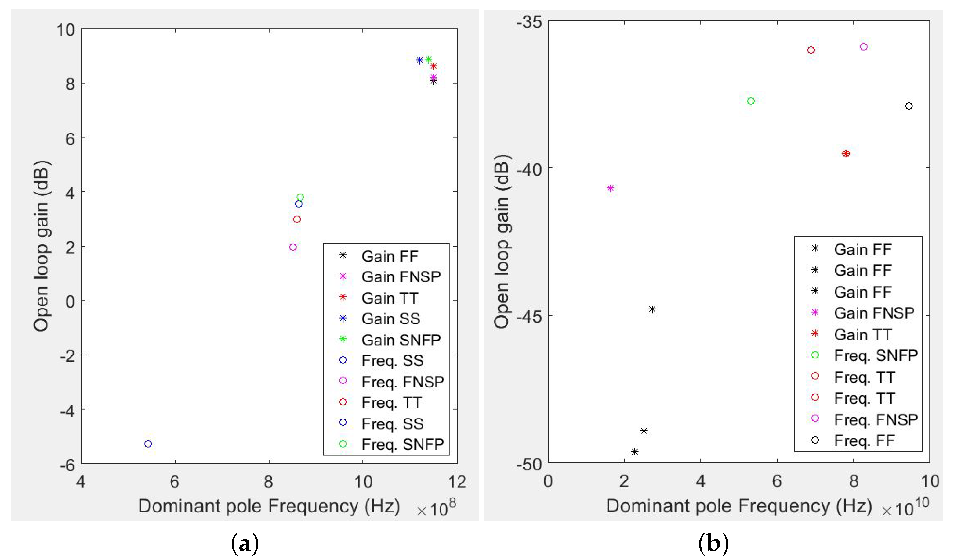
| Corners | Temperature | T− | T | T+ | ||||||
|---|---|---|---|---|---|---|---|---|---|---|
| Voltage | V− | V | V+ | V− | V | V+ | V− | V | V+ | |
| TT | (dB) | 2.98 | 8.64 | 4.05 | 7.07 | −1.7 | −36 | 2.25 | −26 | −39.5 |
| (Hz) | 860 M | 1.2 G | 2.3 G | 1.1 G | 3.1 G | 68.7 G | 1.7 G | 21 G | 78.1 G | |
| SS | (dB) | −5.3 | 3.8 | 8.84 | 3.55 | 7.18 | 3.23 | 5.31 | 4.24 | −20.1 |
| (Hz) | 543 M | 870 M | 1.1 G | 863 M | 1.1 G | 1.81 G | 993 M | 1.4 G | 12 G | |
| SNFP | (dB) | 3.81 | 8.88 | −3.5 | 6.81 | −4.4 | −34.3 | 0.41 | −22.9 | −37.7 |
| (Hz) | 866 M | 1.1 G | 4.6 G | 1.1 G | 4 G | 49.8 G | 1.8 G | 15.3 G | 53 G | |
| FNSP | (dB) | 1.94 | 8.21 | 8.02 | 6.96 | 3.12 | −35.9 | 4.4 | −26 | −40.7 |
| (Hz) | 850 M | 1.2 G | 1.7 G | 1.1 G | 2.1 G | 82.6 G | 1.5 G | 24.6 G | 16.4 G | |
| FF | (dB) | 8.08 | 4.43 | −45 | −4.5 | −38 | −48.9 | −29 | −42 | −49.6 |
| (Hz) | 1.2 G | 2.3 G | 27 G | 4.6 G | 94 G | 25.1 G | 28 G | 16.6 G | 22.6 G | |
| Corners | Temperature | T− | T | T+ | ||||||
|---|---|---|---|---|---|---|---|---|---|---|
| Voltage | V− | V | V+ | V− | V | V+ | V− | V | V+ | |
| TT | (dB) | −9.4 | −2.1 | 5.19 | −0.4 | 7.49 | −22.6 | 4.99 | −2.8 | −36.5 |
| (Hz) | 1.7 G | 2.4 G | 2.1 G | 1.9 G | 1.4 G | 23 G | 1.3 G | 3.5 G | 55 G | |
| SS | (dB) | −16.9 | −7.94 | −1.12 | −5.38 | 0.3 | 9.17 | −0.29 | 6.16 | −6.43 |
| (Hz) | 734 M | 1.6 G | 2.2 G | 1.4 G | 1.7 G | 1 G | 1.4 G | 1.1 G | 4.4 G | |
| SNFP | (dB) | −9.3 | −2.4 | 4.47 | −1.2 | 4.86 | −1.59 | 1.39 | 3.97 | −17.7 |
| (Hz) | 1.8 G | 2.6 G | 2.2 G | 2 G | 1.6 G | 3.5 G | 1.6 G | 1.5 G | 11.1 G | |
| FNSP | (dB) | −9.7 | −1.97 | 5.58 | 0.15 | 9.08 | −34.7 | 7.36 | −22.3 | −45.9 |
| (Hz) | 1.6 G | 2.3 G | 2 G | 1.7 G | 1.2 G | 65.2 G | 1.1 G | 18.8 G | 11.1 G | |
| FF | (dB) | −3.5 | 3.45 | −7.1 | 5.4 | −10.6 | −43.2 | 3.05 | −31.4 | −44.9 |
| (Hz) | 2.6 G | 2.5 G | 10 G | 1.7 G | 9.7 G | 13.3 G | 2.5 G | 39.6 G | 12.7 G | |
| This Work | |||
|---|---|---|---|
| Technology (nm) | 180 | 180 | 180 |
| Number of stages | 4 | 4 | 9 |
| Supply voltage (V) | 1.8 | 1.8 | |
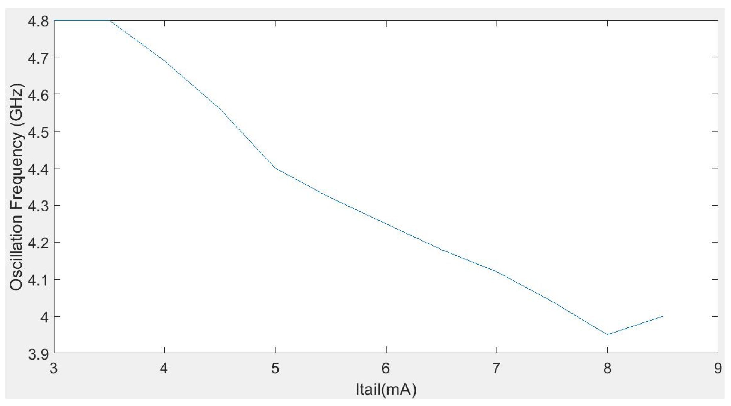
| Tail current (mA) | 4 | 1.4 | 0.145–0.859 |
| Load capacitance (fF) | 50 | 19.7 | - |
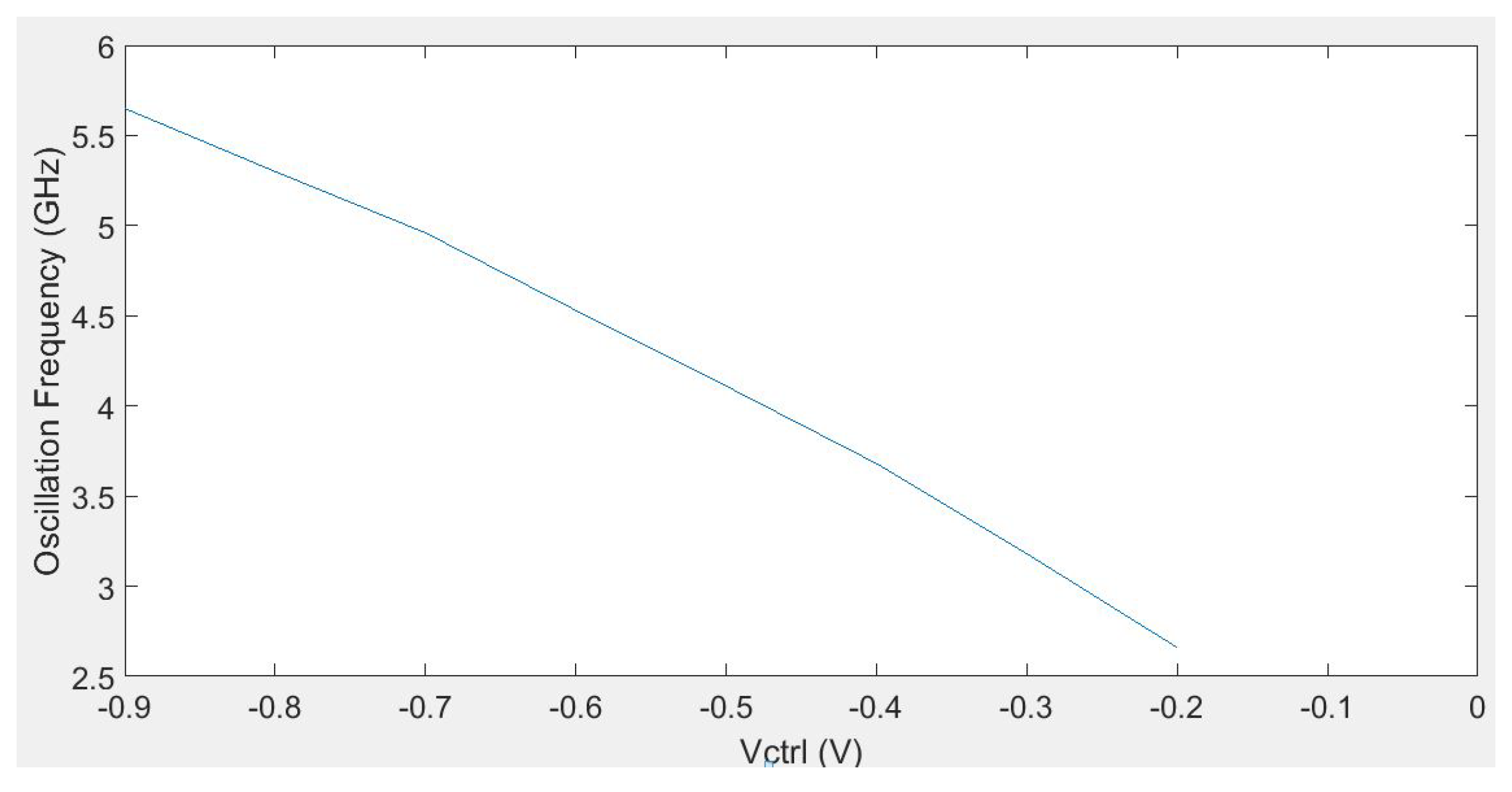
| Freq. tuning range ( GHz) | 2.65–5.65 | 2.2–2.7 | 0.292–1.54 |
| Volt. tuning range (V) | −0.2 to −0.9 | - | 0.6 to 1.8 |
| @-0.9 V Power Diss. (mW) | 44.2 | 10.1 | 0.895 |
| Supply sensitivity | - |
| Current (mA) | s4 | s3 | s2 | s1 |
|---|---|---|---|---|
| 3 | 0 | 1 | 1 | 0 |
| 3.5 | 0 | 1 | 1 | 1 |
| 4 | 1 | 0 | 0 | 0 |
| 4.5 | 1 | 0 | 0 | 1 |
| 5 | 1 | 0 | 1 | 0 |
| 5.5 | 1 | 0 | 1 | 1 |
| 6 | 1 | 1 | 0 | 0 |
| 6.5 | 1 | 1 | 0 | 1 |
| 7 | 1 | 1 | 1 | 0 |
| 7.5 | 1 | 1 | 1 | 1 |
| Characteristic | Pre Layout | Post Layout |
|---|---|---|
| (dB) | 2.49 | 2.49 |
| (Hz) | 1.15 G | 1.15 G |
| (Hz) | 1.02 G | 1.02 G |
| () | 129 | 129 |
| (dB) | −9.92 | −9.92 |
| (dB) | 12.41 | 12.41 |
| (dB) | 11.54 | 11.54 |
| (dB) | −2.5 | −2.5 |
| (V/s) | 349 | 350 |
| (V/s) | −278 | −277 |
| (V) | 0.85 | 0.85 |
| (V) | −0.11 | −0.11 |
| (ps) | 220.1 | 220.1 |
| (ps) | 638.2 | 634.8 |
| (ps) | 999.9 | 999.9 |
| (ps) | 0.05 | 0.05 |
| (s) | 2.3n | 2.3n |
| (V) | 0.75 | 0.75 |
| (V) | −0.1 | −0.1 |
| Corners | Temperature | T− | T | B | ||||||
|---|---|---|---|---|---|---|---|---|---|---|
| Voltage | V− | V | V+ | V− | V | V+ | V− | V | V+ | |
| TT | (dB) | −10.7 | −2.8 | 4.5 | −0.54 | 8.03 | −5.11 | 5.53 | 1.62 | −20 |
| (Hz) | 839 M | 1.3 G | 1.3 G | 1 G | 641 M | 4.2 G | 623 M | 1.1 G | 20 G | |
| SS | (dB) | −23.7 | −14 | −5.1 | −9.3 | −2.7 | 4.31 | −2.8 | 3.52 | 9.36 |
| (Hz) | 145 M | 132 M | 969 M | 580 M | 841 M | 832 M | 666 M | 696 M | 215 M | |
| SNFP | (dB) | −10.7 | −3.2 | 3.1 | −1.96 | 3.68 | 3.9 | 0.12 | 3.15 | −3.8 |
| (Hz) | 871 M | 1.3 G | 1.4 G | 1.1 G | 919 M | 497 M | 936 M | 569 M | 1.5 G | |
| FNSP | (dB) | −10.2 | −2 | 6.34 | 0.85 | 11.1 | −20 | 10.5 | −18 | −26 |
| (Hz) | 837 G | 1.3 G | 1.1 G | 969 M | 432 M | 28 G | 368 M | 16 G | 62 G | |
| FF | (dB) | −0.07 | 8.89 | −13 | 7.1 | −15 | −25 | −8.4 | −22 | −27 |
| (Hz) | 1.6 G | 851 M | 17 G | 276 M | 16 G | 60 G | 4.5 G | 28 G | 60 G | |
© 2019 by the authors. Licensee MDPI, Basel, Switzerland. This article is an open access article distributed under the terms and conditions of the Creative Commons Attribution (CC BY) license (http://creativecommons.org/licenses/by/4.0/).
Share and Cite
Tlelo-Cuautle, E.; Castañeda-Aviña, P.R.; Trejo-Guerra, R.; Carbajal-Gómez, V.H. Design of a Wide-Band Voltage-Controlled Ring Oscillator Implemented in 180 nm CMOS Technology. Electronics 2019, 8, 1156. https://doi.org/10.3390/electronics8101156
Tlelo-Cuautle E, Castañeda-Aviña PR, Trejo-Guerra R, Carbajal-Gómez VH. Design of a Wide-Band Voltage-Controlled Ring Oscillator Implemented in 180 nm CMOS Technology. Electronics. 2019; 8(10):1156. https://doi.org/10.3390/electronics8101156
Chicago/Turabian StyleTlelo-Cuautle, Esteban, Perla Rubi Castañeda-Aviña, Rodolfo Trejo-Guerra, and Victor Hugo Carbajal-Gómez. 2019. "Design of a Wide-Band Voltage-Controlled Ring Oscillator Implemented in 180 nm CMOS Technology" Electronics 8, no. 10: 1156. https://doi.org/10.3390/electronics8101156
APA StyleTlelo-Cuautle, E., Castañeda-Aviña, P. R., Trejo-Guerra, R., & Carbajal-Gómez, V. H. (2019). Design of a Wide-Band Voltage-Controlled Ring Oscillator Implemented in 180 nm CMOS Technology. Electronics, 8(10), 1156. https://doi.org/10.3390/electronics8101156