


Abstract
In conventional CLLC topologies, CC/CV charging is typically implemented using closed-loop control strategies based on phase shift modulation. This not only increases control complexity but also requires additional voltage and current sensing circuits, thereby raising the overall system cost. To address these issues, this paper proposes a novel CC/CV charging strategy. By analyzing the inherent characteristics of the coupled network, the switching frequencies corresponding to the CC and CV operating points are derived. By jointly applying frequency modulation and phase shift control to the CLLC converter, the system not only realizes CC/CV charging, but also enables the regulation of both the magnitude and the direction of power flow. Furthermore, to improve the system’s efficiency, a fine frequency tuning method is introduced to ensure operation under the critical zero-voltage switching (ZVS) condition. Finally, a 500 W prototype is constructed to validate the effectiveness of the proposed control strategy.
1. Introduction
With the rapid growth of electric vehicles (EVs), energy storage systems (ESSs), and data centers, DC power supply architectures are becoming increasingly prevalent [1,2,3,4]. In this context, bidirectional DC–DC converters, which provide efficient power exchange between DC buses operating at either different or identical voltage levels, are widely deployed in Low-Voltage DC (LVDC), Medium-Voltage DC (MVDC), and High-Voltage DC (HVDC) systems. Because bidirectional power flow is required, conventional unidirectional topologies employing passive rectification, such as phase shifted full-bridge converters [5] and LLC resonant converters [6], are no longer adequate. Instead, dual active bridge (DAB) converters with active secondary-side structures [7,8], as well as LLC/CLLC resonant converters equipped with active rectifiers [9,10,11], have become mainstream solutions.
Nevertheless, DAB converters exhibit several inherent limitations. Under light load conditions, the circulating current is often insufficient to guarantee ZVS during the dead time [12,13,14], and phase shift feedback control is typically required to maintain a constant voltage gain [15]. In contrast, the CLLC series resonant converter offers more favorable characteristics: its resonant tank current is relatively large, enabling ZVS over the full load range, and a nearly constant voltage gain can be maintained around the resonant frequency without closed-loop regulation [16,17,18,19]. As a result, a simpler overall system architecture can be achieved.
The battery charging process generally consists of CC and CV stages, during which the equivalent load varies over a wide range [20]. Traditional modulation strategy pulse frequency modulation (PFM) can hardly deal with the CC mode over a wide range, as it can bring problems such as high switching and core losses [21,22]. In addition, the CV mode is a light load condition to the CLLC converter, and PFM cannot realize voltage regulation and it will reduce the efficiency of the converter under the light condition [23,24]. To deal with these problems, many strategies such as hysteretic burst [25] and asymmetric pulse width modulation (APWM) [26] have been proposed. Although these strategies have the advantages of higher efficiency or better voltage regulation than PFM under light load conditions, they cannot deal well with heavy load conditions. Triple-phase shift (TPS) modulation is proposed to reduce the resonant current on both sides of transformer, thereby improving the system’s efficiency [27] under the same output power conditions during CV stage. Compared to other improved strategies, although the combination of PFM and dual-side phase shift control has already been proposed to charge the battery [28], TPS modulation has a sufficient output voltage range and high efficiency during the whole charging process, so it can deal with both the light or heavy condition mode individually. However, to regulate both the magnitude and direction of power flow across such a broad operating range, the control strategy using TPS modulation typically relies on complex voltage and current sensing networks, along with the real-time adjustment of the phase shift angle to track the CC/CV charging profile of the battery [29,30]. This not only increases control complexity and hardware cost, but may also introduce additional stability concerns [31,32,33]. To alleviate these issues, this paper proposes an open-loop control strategy based on a CLLC resonant converter. By exploiting the distinctive gain characteristics of the CLLC converter, CC and CV operation are naturally realized by switching among analytically determined resonant operating points, thereby closely matching the requirements of battery charging. Without any voltage or current feedback loops, the converter is regulated solely through switching frequency modulation, which significantly simplifies the system architecture, enhances reliability, and reduces cost.
Beyond enabling the streamlined realization of CC/CV charging, the proposed strategy also provides excellent soft switching performance. By finely tuning the switching frequency in the vicinity of the predefined CC/CV frequency points, the converter can be consistently operated at the boundary of critical soft switching. In contrast to conventional soft switching schemes based on phase shift control, the critical soft switching conditions in the proposed approach admit explicit analytical relationships with circuit parameters such as dead time and load current, rather than relying on numerical iterative procedures. This analytical characterization offers clear insight for parameter selection, loss optimization, and load adaptivity evaluation.
In summary, this paper presents an open-loop CLLC resonant converter scheme for battery CC/CV charging based on frequency modulation. The proposed approach features reduced control complexity, improved soft switching performance, and analytically tractable design criteria, making it attractive for high-performance bidirectional DC power conversion applications.
The main contributions of this paper are summarized as follows:
- By exploiting the distinctive gain characteristics of the CLLC converter, the proposed strategy naturally realizes CC and CV charging operation without relying on complex voltage and current sensing networks or feedback loops. This significantly simplifies the system architecture, enhances reliability, and reduces the overall hardware cost.
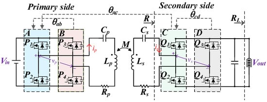
- By jointly applying frequency modulation and phase shift control to the CLLC converter, the system successfully enables the regulation of both the magnitude and the direction of power flow. Specifically, the bilateral internal phase shift angles θab and θcd are utilized to regulate the magnitude of the active power flow, whereas the external phase shift angle θac is employed to control its direction.
- A critical ZVS condition is proposed to avoid body diode conduction and minimize conduction losses. Furthermore, the critical soft switching conditions in this approach admit explicit analytical relationships with circuit parameters, allowing the exact switching frequency perturbation Δf to be calculated without relying on numerical iterative procedures.
2. Output Characteristics of CLLC Converter Under Different Tuning Schemes
2.1. Output Gain Analysis
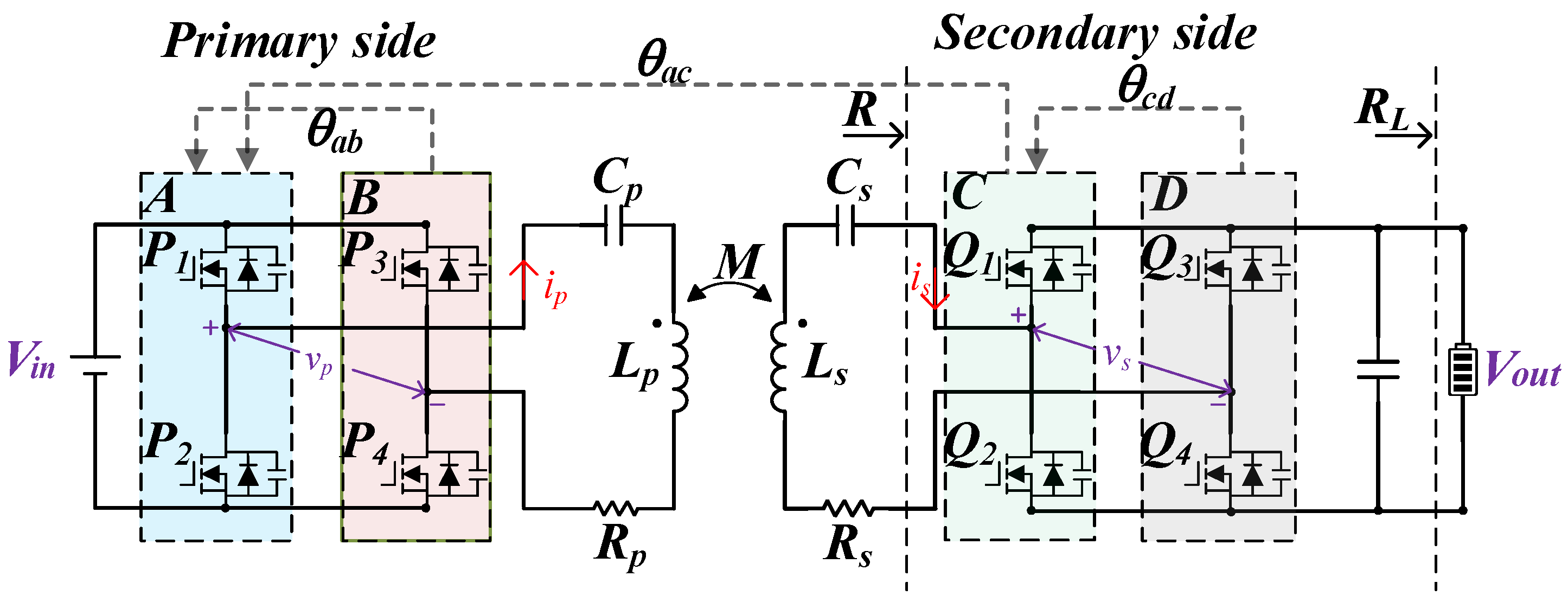
As shown in Figure 1, the bidirectional CLLC resonant converter interfaces a DC bus with input voltage Vin and a battery load through a dual active bridge stage and a high-frequency coupling network. The dual active bridge consists of primary-side half-bridges A and B and secondary-side half-bridges C and D. The coupling network is realized by two resonant capacitors Cp and Cs and a high-frequency transformer characterized by inductances Lp and Ls, mutual inductance M, and winding resistances Rp and Rs. During the charging process, the battery pack is modeled as an equivalent load resistance RL, which varies with the operating condition.
Figure 1.
Scheme diagram of bidirectional CLLC resonant converter.
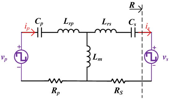
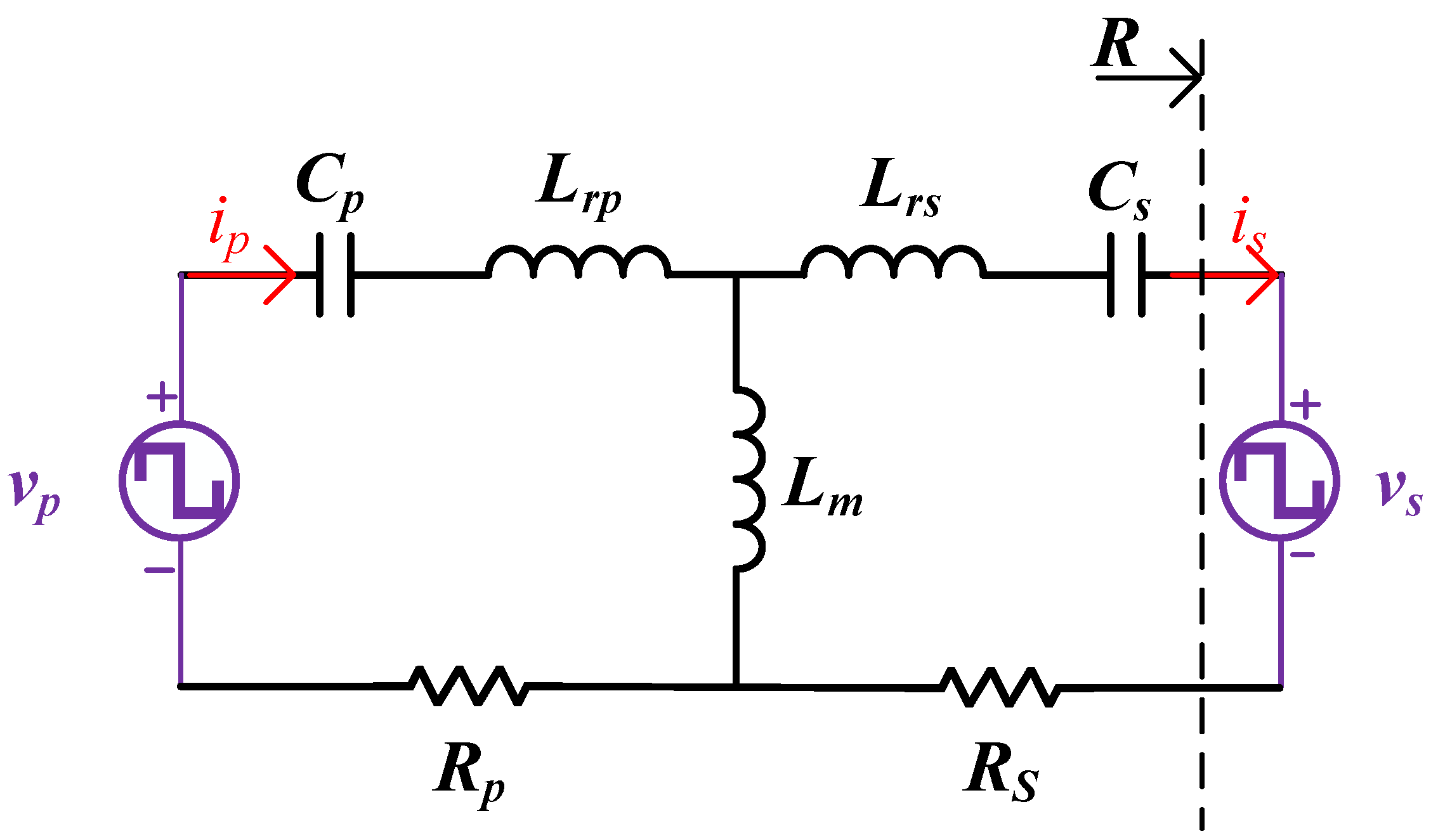
When the parameters of the coupling network are fixed, the intrinsic characteristics of the CLLC resonant tank depend solely on the operating frequency and the load condition. To analyze these characteristics, the original schematic can be reduced to the simplified equivalent circuit shown in Figure 2. In this model, the transformer is represented by series inductances Lrp = Lp − M and Lrs = Ls − M, and a parallel magnetizing inductance LT = M. To ensure that both the Lp − Cp and Ls − Cs branches resonate at the specified frequency fr, the resonant elements are designed such that , and thus Cp and Cs are selected according to the given values of Lp and Ls, respectively. The dual active bridge stages are replaced by a fundamental input voltage source vp(1) and an equivalent load resistance R = 8/π2RL.
Figure 2.
Equivalent circuit of the CLLC resonant converter.
By transforming the equivalent circuit in Figure 2 into the frequency domain, the relationships between the fundamental components of the input and output quantities can be explicitly derived. The ratio of the fundamental output voltage to the fundamental input voltage is defined as the voltage gain Gvv(jw), while the ratio of the fundamental output current to the fundamental input voltage is defined as the current gain Gvi(jw). Their analytical expressions are given in (1) and (2).
where
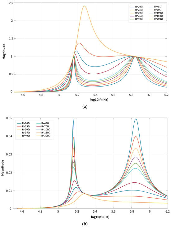
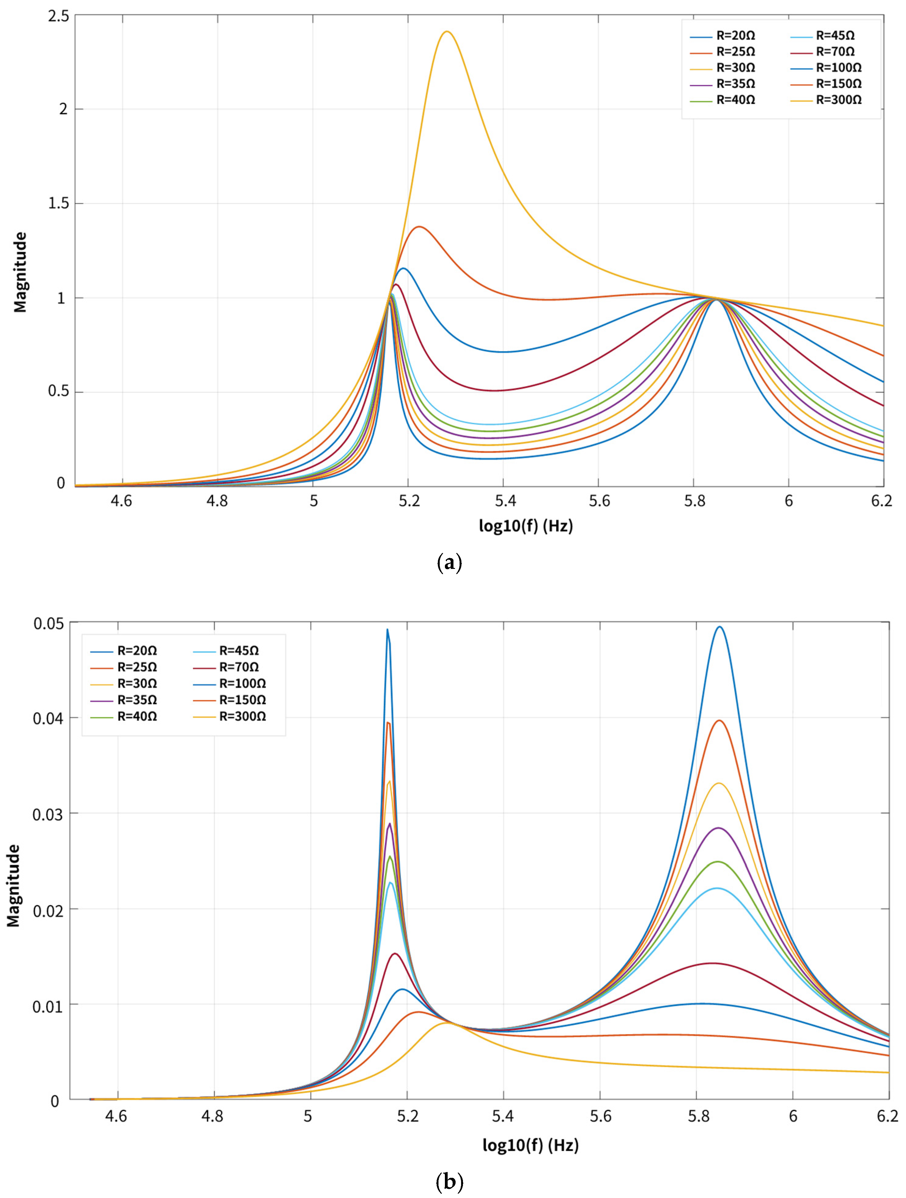
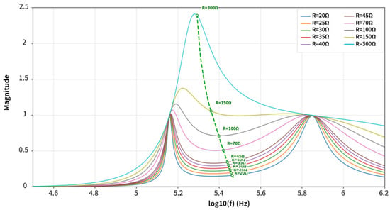
As illustrated in Figure 3, the output gain curves clearly reveal the intrinsic characteristics of the coupling network. In the Gvv(jω) curve, the family of trajectories obtained by varying the equivalent resistance Ro intersects at two frequencies (CV Points) [34]. Define the higher of these two intersection frequencies as fr. The Gvi(jω) curve exhibits a single intersection CC point, and the corresponding frequency is .
Figure 3.
Output gain characteristic curve of the system. (a) Curves of Gvv(jw) on different loads. (b) Curves of Gvi(jw) on different loads.
2.2. Final Stage
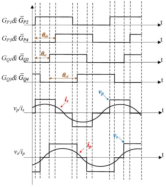
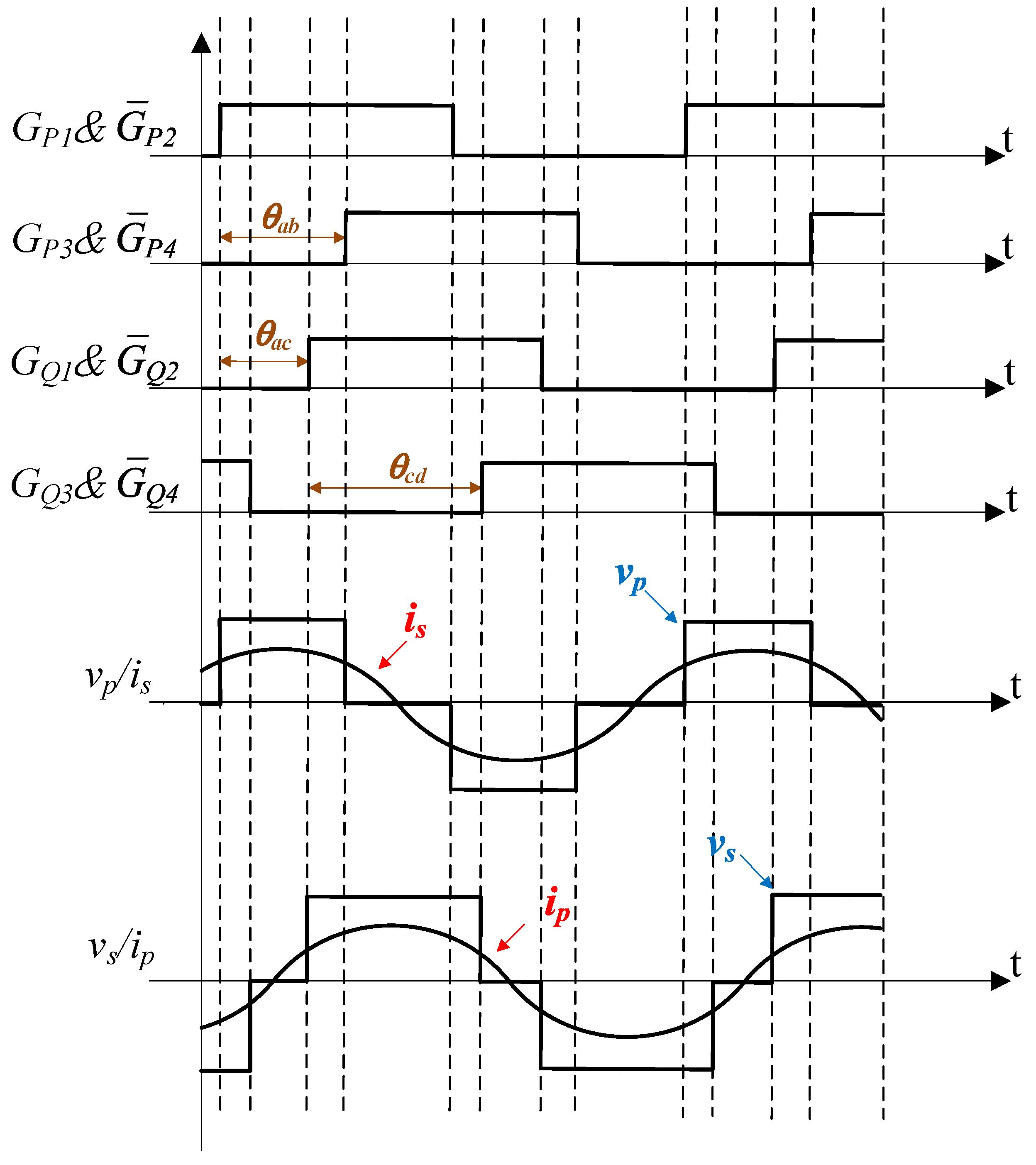
Figure 4 illustrates the gate drive signals of the active switches in the four half-bridges A, B, C, and D. In each half-bridge, the upper and lower switches are driven in a complementary manner, each conducting for 180°. Taking half-bridge A as the reference, the gate signals of B and C lag by angles θab and θcd, respectively, while the gate signal of D lags that of C by θac.
Figure 4.
Bilateral phase shift control strategy.
The Fourier expressions of input and output voltage of the couple network are given as follows:
Considering only the fundamental components vp(1) and vs(1) of vp and vs, the complex forms and are given as follows:
By writing the KCL and KVL equations in Figure 2, (7) and (8) can be obtained. There
and is the complex form of primary current ip and secondary current is.
Operating at the CC point with frequency fT, the current
can be obtained by solving (8) and (9) simultaneously, the expression of which is shown as follows:
The input active, reactive power and output active power of the circuit can be calculated from
and , as shown in (10)–(12):
It can be observed that the internal phase shift angles θab, θcd, and θac have nearly identical effects on both active and reactive power. In contrast, the external phase shift angle provides an additional degree of freedom to achieve the desired magnitude and direction of the active power while simultaneously reducing the reactive power. Therefore, θab and θcd are utilized to regulate the magnitude of the active power flow, whereas θac is employed to control its direction. Once the direction of power flow is determined, the voltage source on the receiving side can be represented by an equivalent resistance Ro, whose value is given in (13):
Based on this equivalent representation, the active and reactive power of the system operating at the CV point with frequency fr can be obtained in the same manner as for the CC operating point discussed above.
3. Battery CC/CV Charging Strategy Under Different Resonant Tuning Scheme
3.1. Dual-Side Phase Shift Zero-Phase Angle Control
Reactive power circulating in the system increases the conduction losses rather than delivering useful power to the load. To avoid this, the system should operate under the Zero-Phase Angle (ZPA) condition. The CC operating point inherently satisfies the ZPA condition, whereas the CV point operates close to ZPA [35]. When phase shift control of the dual active bridge is introduced, however, considerable reactive power may appear if the internal phase shift angles θab and θcd do not satisfy a specific relationship with the external phase shift angle θac.
According to (5) and (6), θab and θcd change both the magnitude and phase of the input and output the voltage of coupling network, while θac only changes the phase. When the system operates in the CV mode, the introduction of internal and external phase shift angles must produce an equal magnitude and phase of the input voltage and output voltage of the coupling system to retain the characters of the CV point of the coupling network. Thus θab, θcd and θac must satisfy the condition given as follows:
When the system operates in the CC mode [36], θab, θcd and θac must satisfy the condition given by (16).
It is noteworthy that, in CC mode, no specific magnitude relationship between the input and output voltages of the coupling network is required, since this relationship is load dependent. Furthermore, when the internal and external phase shift angles satisfy (16) at the CC operating point, the primary-side reactive power becomes zero according to (12). Hence, the overall system preserves the ZPA condition inherent to the coupling network at the CC point, thereby validating the above analysis.
3.2. Critical ZVS Condition
To achieve ZVS, the primary current ip in the coupling network must flow through the MOSFET parasitic capacitor Coss during the dead time and fully discharge the stored charge Qε = CossVdc, as given in (17). This requirement implies that the system must exhibit an inductive characteristic.
Although a longer time to discharge the parasitic capacitor makes ZVS easier to achieve, the primary current ip then flows through the body diode during the remaining dead time. This increases the conduction losses, thereby reducing the system’s efficiency. Therefore, critical ZVS on the primary-side MOSFETs is required, meaning that the parasitic capacitor is fully discharged exactly at the end of the dead time, so that body diode conduction is avoided.
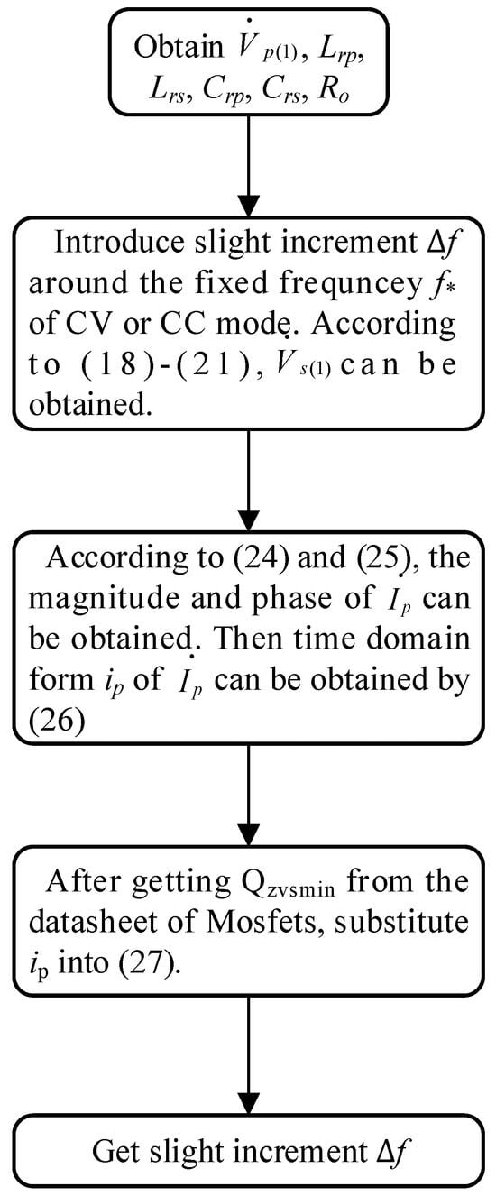
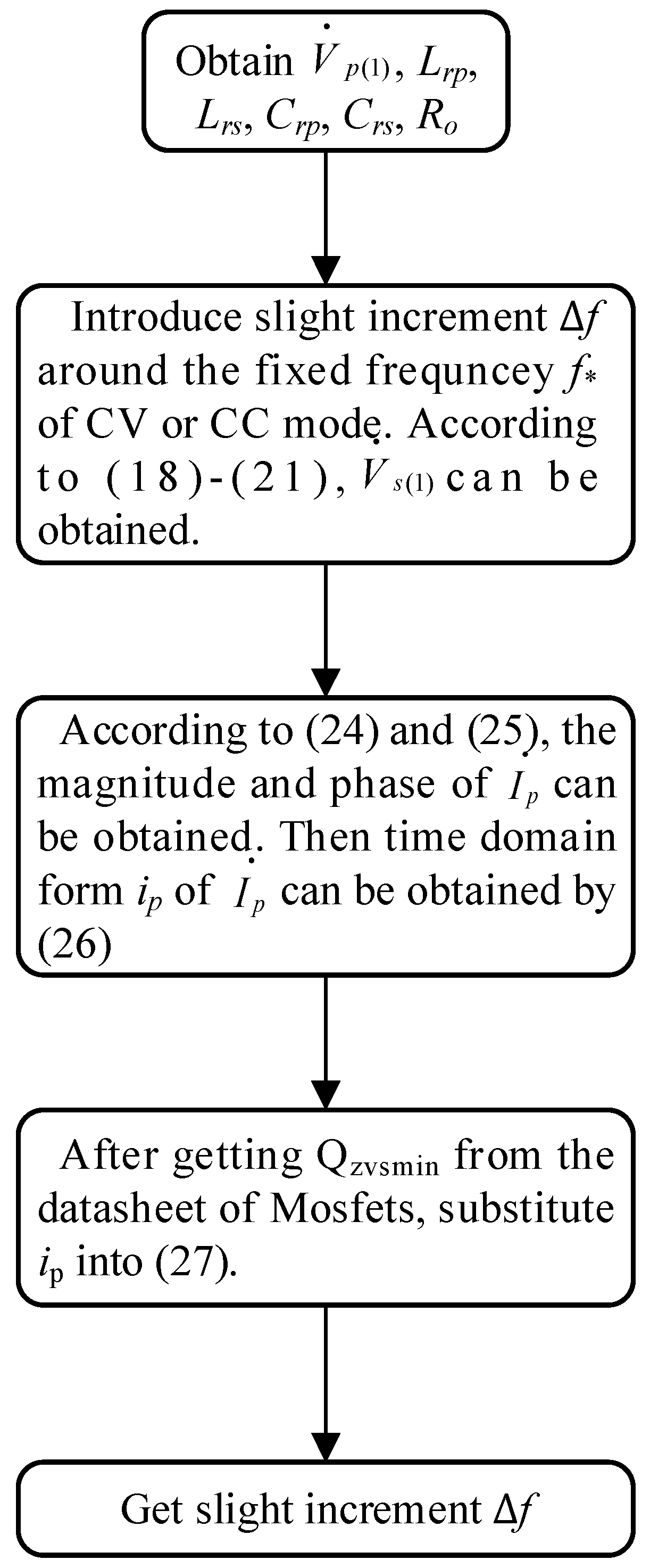
The critical ZVS condition depends on the dead time of the primary half-bridge and the primary current ip flowing through Coss. For a given dead time tdead and a specified MOSFET type, the required magnitude of ip is determined by (17). However, the equivalent battery resistance RL varies over a wide range in the CC and CV charging modes, which in turn affects the magnitude of ip. To maintain the critical ZVS in both the CC and CV modes, a slight frequency perturbation Δf around the switching frequency fT or fr, depending on the operating mode, is introduced to regulate ip to the required value. Using the CV mode as an example, Figure 5 shows the procedure to determine the necessary Δf when RL changes. Once the system parameters Cp, Cs, Lrp, Lrs, and Lm, and the input equivalent resistance of the secondary active bridge are specified, the magnitude and phase of the voltage gain Gvv(jw) can be obtained by (1). The magnitude and phase of are determined by (18) and (19).
where
Figure 5.
Calculation procedure for critical soft switching frequency fine-tuning.
According to the definition of the voltage gain Gvv(jw), the fundamental component vs(1) of the output voltage of the coupling network can be obtained from (20) and (21).
By using the equivalent circuit in Figure 2, (22) and (23) can be listed. Then,
can be obtained by solving (23), and the magnitude and phase can be obtained from (24) and (25).
Notice that
and θ′ are not only the magnitude and phase of the complex number
but are also the root mean square value and initial phase of the current on the primary side; the time-domain expression of the current can be obtained from (26). Here, f* + Δf is the switching frequency of the Mosfets. The value of can f* be fr in the CV mode or fT in the CC mode. Δf is the slight perturbation around f*, which has been already explained.
Then combining the equations from (17) to (26) and setting tdead to be 3% of 1/(f* + Δf), (27) can be obtained as follows:
There Qzvsmin is equal to Qɛ, which is the minimum charge needed to discharge to realize ZVS when ip flows through Coss. According to (27), the required frequency perturbation Δf depends not only on R, but also on vp(1) and the coupling network’s parameters. The primary internal phase shift angle θab and the DC bus voltage determine vp(1), whereas the secondary internal phase shift angle θcd affects R.
Consequently, variations in the internal phase shift angles, DC bus voltage, load resistance, and coupling network parameters all necessitate a fine adjustment of the switching frequency to maintain the critical ZVS. The impact of these factors on Δf can be quantitatively evaluated using (27).
Based on the system parameters listed in Table 1, the Gvv(jω) curve can be drawn and the critical soft switching trajectories under different operating conditions in the CC mode, which is taken as an example, can be plotted by following the calculation procedure in Figure 5, as shown in Figure 6, which serves to guide the controller to achieve a high-efficiency soft switching operation over the entire operating range.
Table 1.
Parameters of the coupling network of CLLC converter.
Figure 6.
Critical soft switching trajectory.
3.3. Control Block
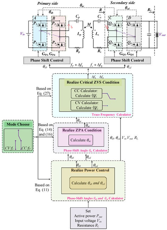
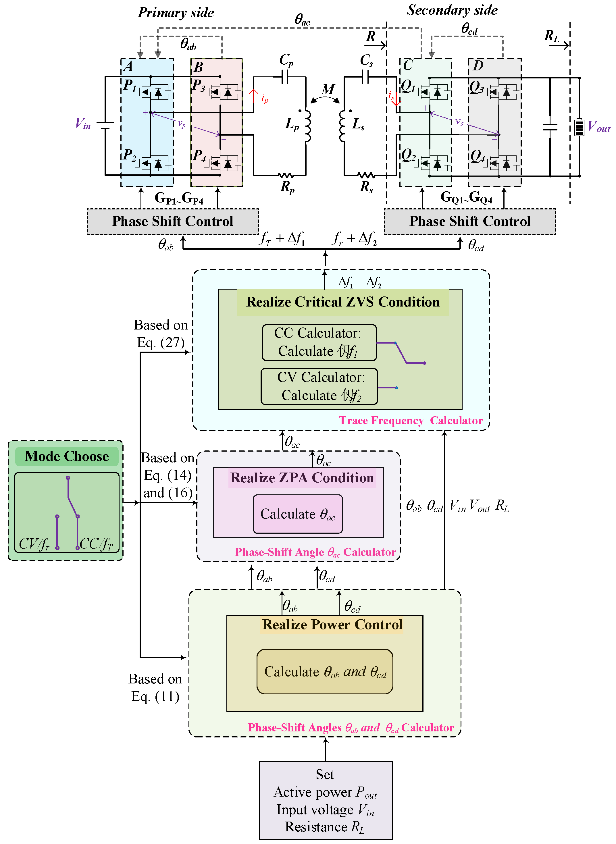
The proposed system in Figure 7 enables bidirectional power transfer with the unified regulation of both the power magnitude and direction, while supporting CC/CV charging as well as critical soft switching operation. The overall control procedure is summarized as follows. First, the controller selects either the CC or CV mode according to the operating condition and charging requirement. After checking the required active output power Pout, input voltage Vin and resistance RL, the transferred power is regulated based on (11). When the converter works in the CC mode, Pout and the max efficiency condition [36] determine the external phase shift angles θab and θcd definitively, while in the other mode the bilateral internal phase shift angles θab and θcd are also determined to achieve the accurate control of bidirectional power flow by considering the constraint of the DC transformer with a turn ratio of one and using (11). Then external phase shift angle θac is obtained by (14) in CV mode or (16) in CC mode. Furthermore, to reduce switching losses and improve conversion efficiency, the switching frequency is fine-tuned according to (27) so that the converter operates at the boundary of soft switching. As a result, critical soft switching is realized, leading to enhanced efficiency over a wide operating range.
Figure 7.
Overall control block diagram of the system.
It should be noted that, in a bilateral power conversion system, both the regulation of the external phase shift angle and the adjustment of the switching frequency may introduce a reactive power component, thereby affecting the current/voltage phase relationship, soft switching margin, and device stress. Considering that, under the developed analytical model, frequency modulation allows a more straightforward derivation of closed-form solutions and provides a convenient means to continuously shape the reactive power with limited implementation complexity, this work adopts switching frequency tuning as the primary approach to inject the required reactive power for achieving critical soft switching.
Accordingly, a specific outer phase shift is first selected to enforce the ZPA condition of the bilateral system, establishing a baseline operating point with negligible reactive power. Subsequently, the switching frequency is fine-tuned around this ZPA point to introduce a controlled amount of reactive power and to reshape the phase relationship, thereby enabling and maintaining soft switching operation with improved efficiency.
4. Prototype Implementation and Experimental Verification of the Bidirectional CLLC Resonant Converter System
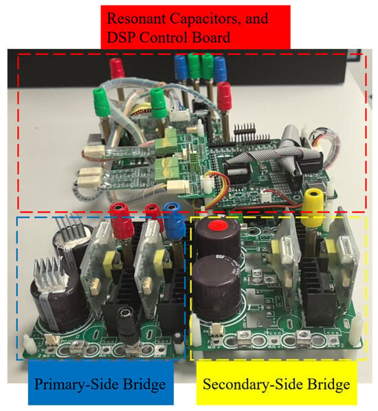
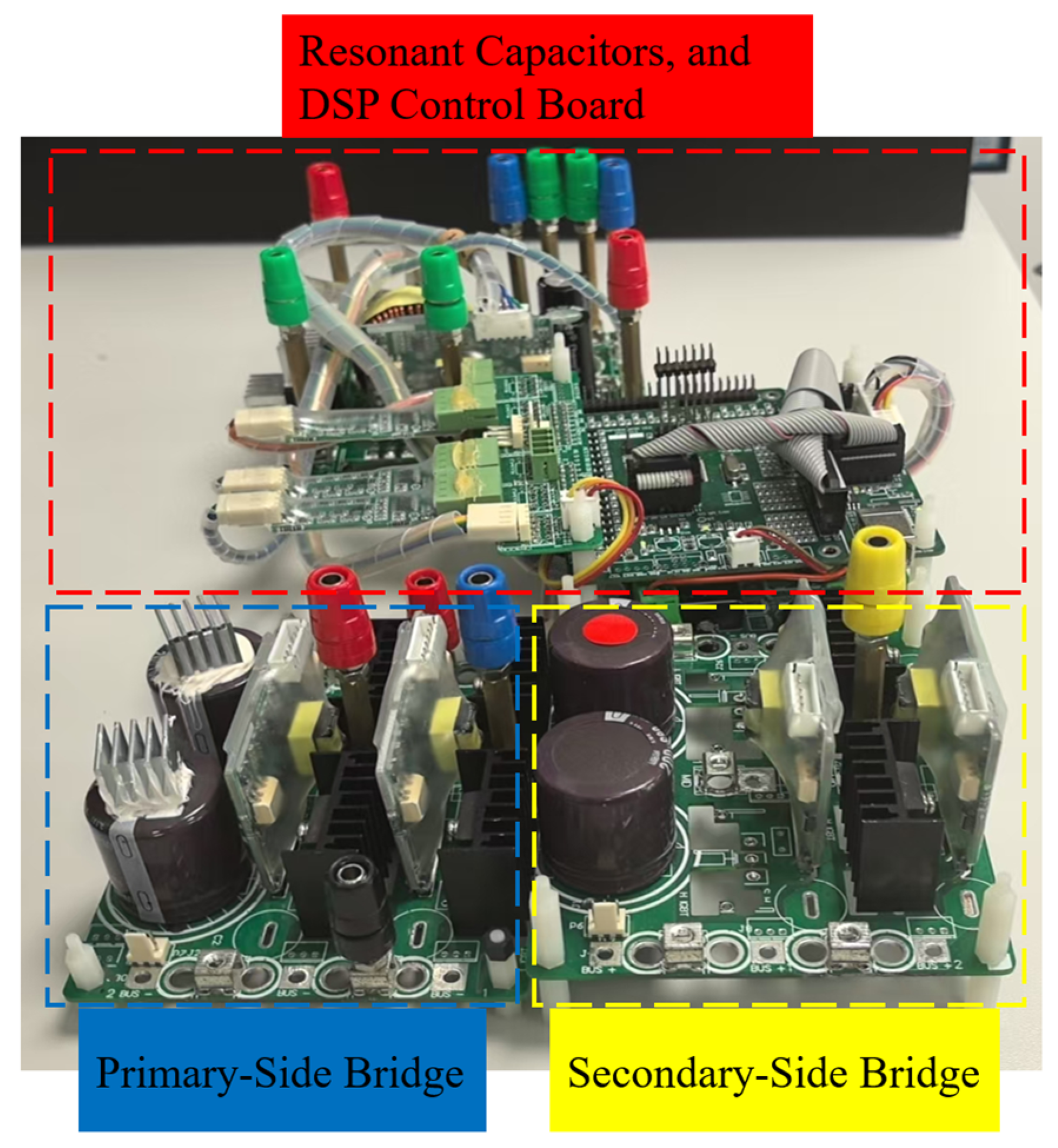
In Section 3, the conditions to realize dual-side ZPA control and the procedure to calculate the trace frequency to realize critical ZVS have been derived. To verify the realization of the power flow control and the ZPA condition during the power control, and to show the experimental measurement of the value of the fine-tuning frequency ∆f, a 500 W laboratory prototype of the bidirectional CLLC resonant converter was built, which is shown in Figure 8. The detailed parameters and specifications of the prototype are listed in Table 2.
Figure 8.
Experimental prototype.
Table 2.
Parameters and specifications of the prototype.
To bridge the theoretical derivations and the hardware implementation, DSP executes the proposed analytical model to generate real-time control signals. Specifically, upon acquiring the equivalent load resistance and determining the operating mode, the controller calculates the bilateral internal phase shift angles θab and θcd, based on the active power transfer requirements formulated in (11). Subsequently, to enforce the ZPA condition and mitigate circulating reactive power, the external phase shift angle θac is analytically determined using (14) for the CV mode and (16) for the CC mode. Finally, to guarantee critical ZVS operation and improve conversion efficiency, the switching frequency fine-tuning component, Δf, is computed according to (27). These sequentially evaluated parameters are directly utilized by the DSP to generate the corresponding PWM signals for the switching devices, effectively translating the theoretical control laws into practical converter operation.
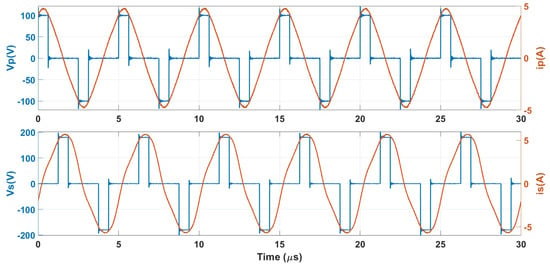
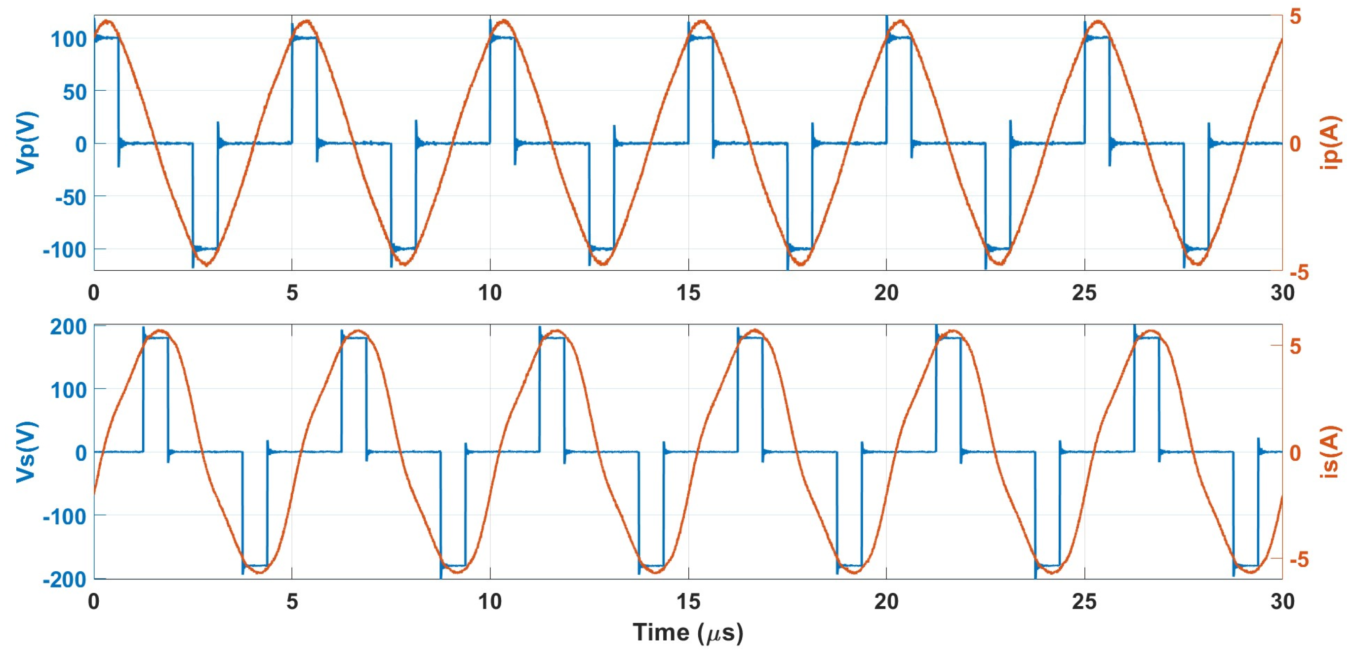
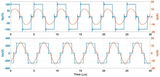
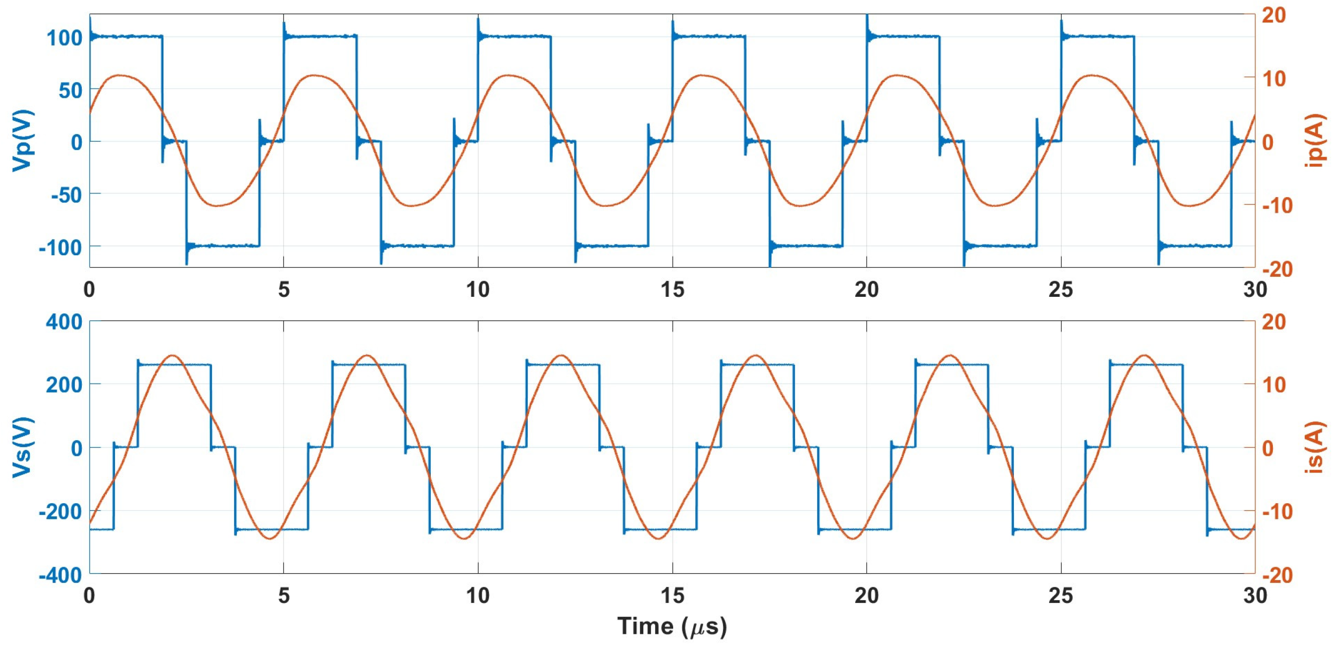
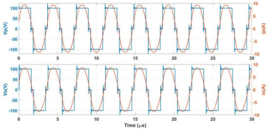
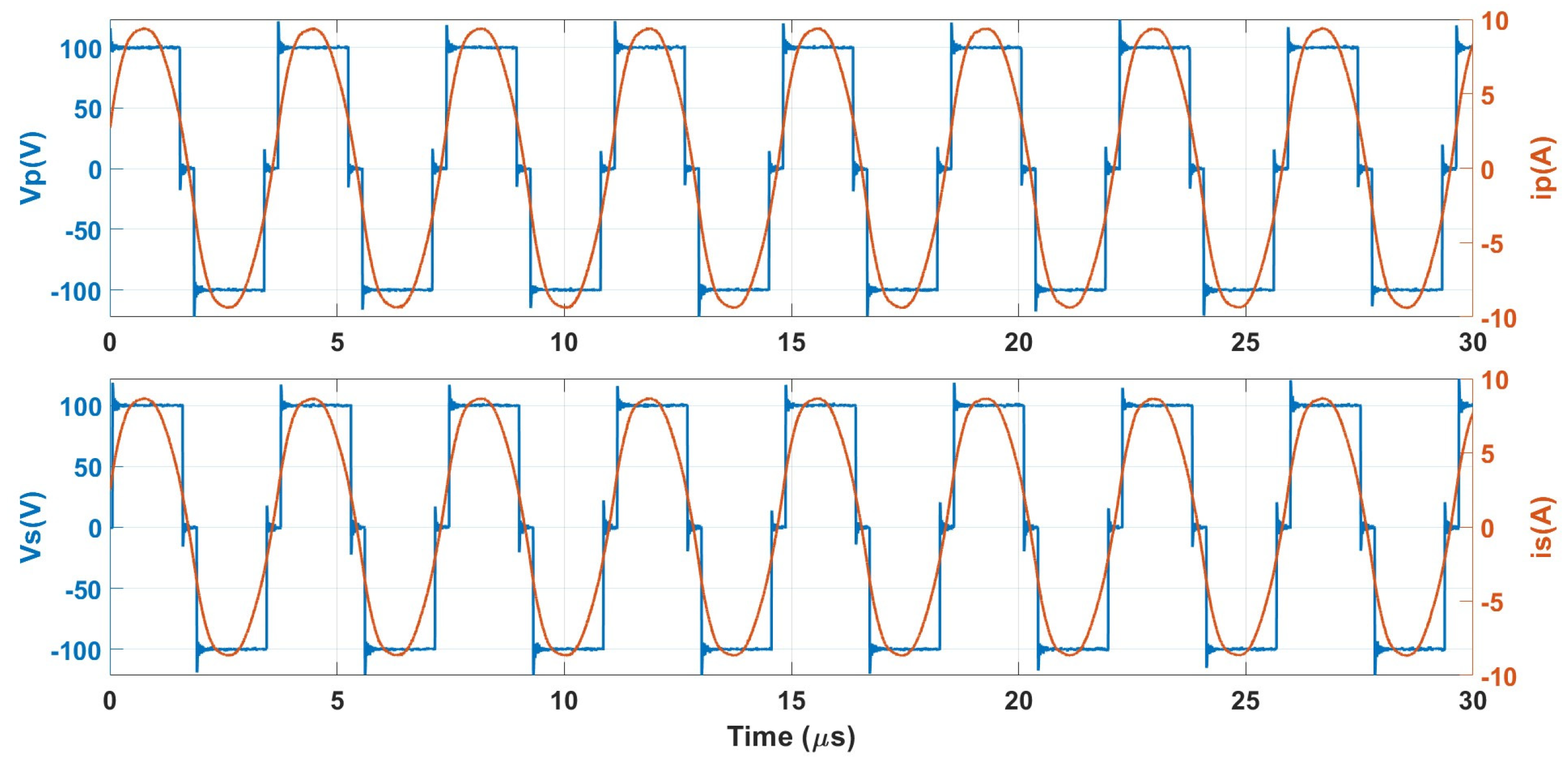
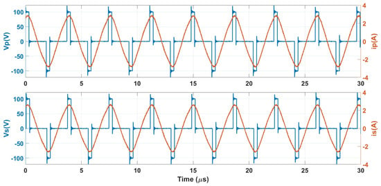
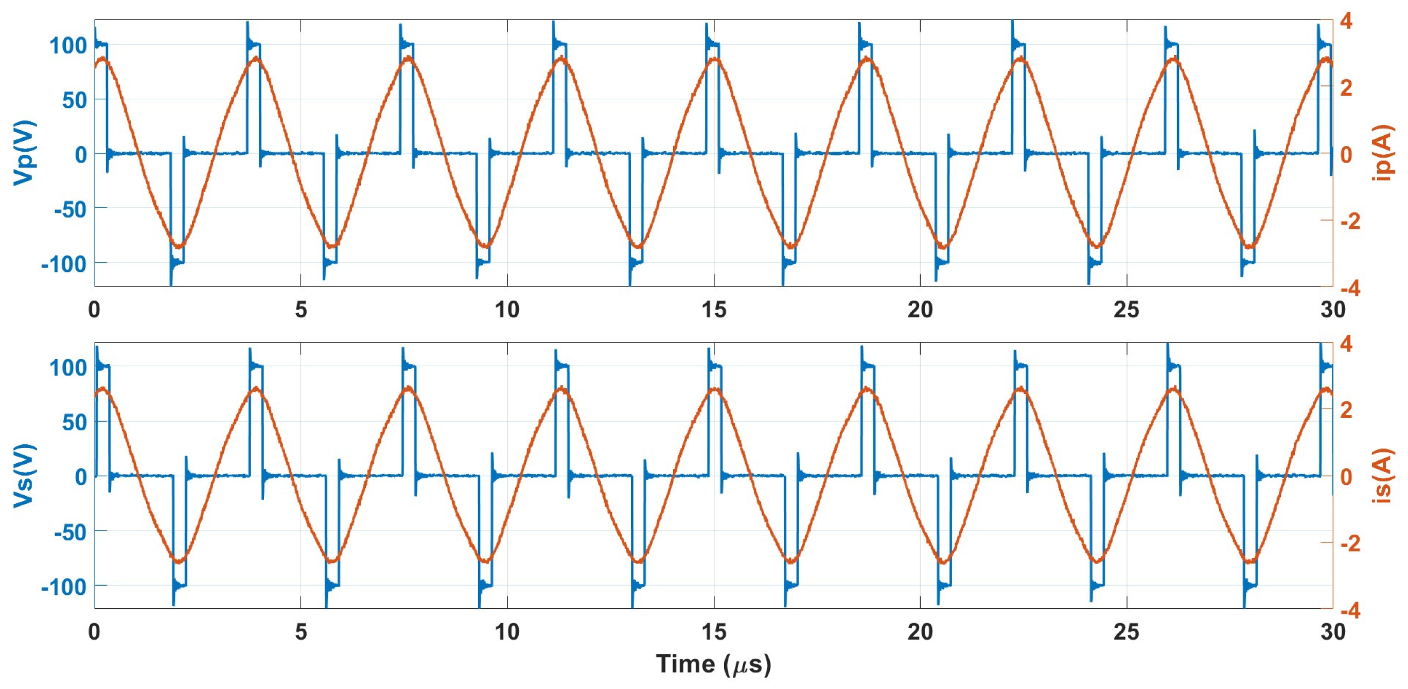
The experiments first verify the capability of regulating the transferred power magnitude. The converter is operated in the CC mode. As evidenced by the measured waveforms in Figure 9 and Figure 10, when the internal phase shift angles on the primary and secondary sides are set to be equal, the bridge voltages exhibit an approximately 90° phase displacement, which is consistent with the expected phase relationship at this operating point. Moreover, by varying the internal phase shift angle on the primary side, the transmitted power can be continuously regulated, confirming the effectiveness of the proposed power control mechanism. In addition, the outer phase shift angle is adjusted to enforce the ZPA condition of the bilateral system, thereby establishing a suitable operating point for the subsequent high-efficiency soft switching operation.
Figure 9.
Low-duty-ratio waveforms in CC mode.
Figure 10.
High-duty-ratio waveforms in CC mode.
When the converter operates in the CV mode, the output gain characteristic indicates that it works at a unity gain operating point. With the internal phase shift angles on the primary and secondary sides set to be identical, the experimental results in Figure 11 and Figure 12 show that the voltages and currents on both sides are in phase, and their magnitudes are nearly identical. By exploiting this inherent output characteristic, the proposed strategy provides an effective and implementation-friendly solution for 1:1 DCX (DC transformer) applications.
Figure 11.
High-duty-ratio waveforms in CV mode.
Figure 12.
Low-duty-ratio waveforms in CV mode.
For the validation of critical soft switching, the analytical model and closed-form derivations developed in the previous sections yield the critical soft switching trajectory depicted in Figure 6, which defines the theoretical boundary under different operating conditions.
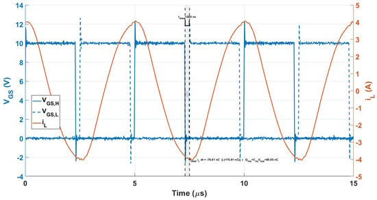
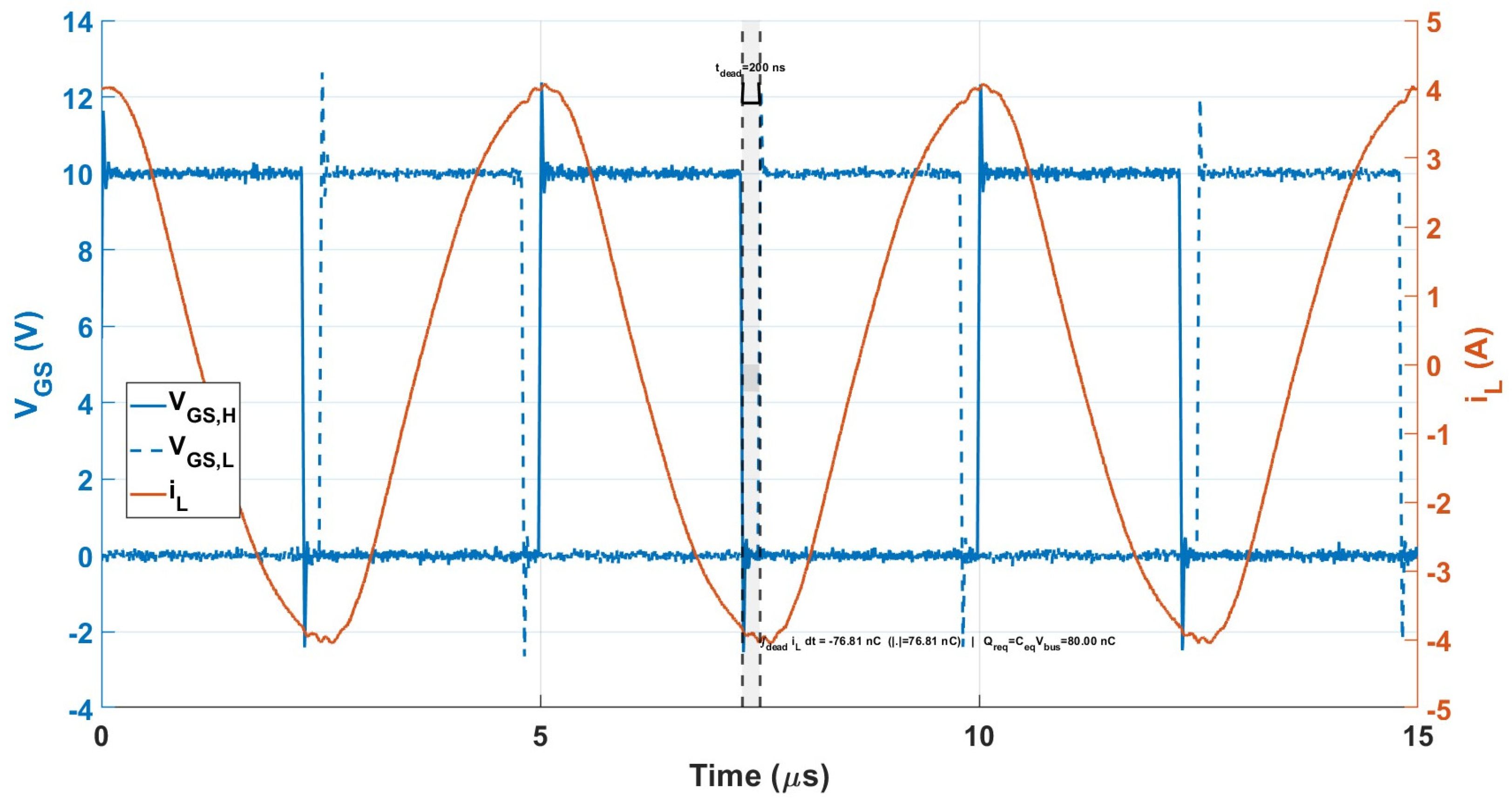
For the practical identification of the critical soft switching operating point, Figure 13 illustrates the measurement-based procedure: the resonant tank current is integrated over the dead time to estimate the charge available for commutating the switching node. By progressively matching this charge to that required for charging the switch output capacitance, the critical switching frequency operating point can be determined.
Figure 13.
Critical soft switching point calculation for the switch.
To witness the advantage of the proposed strategy on efficiency improvement, there is a comparative analysis against the conventional fixed-frequency phase shift control under identical operating conditions (Vin = 100 V; Po = 500 W) in CV mode. The analysis indicates that the proposed strategy—by tracking the unity gain frequency—reduces the resonant tank RMS current by approximately 17% and the AC reactive power by ~40% due to the minimized phase difference. Consequently, the overall efficiency at the rated load is improved by 1.5–2.8% due to the reduced circulating current and maintained ZVS.
To further clarify the mechanism of efficiency improvement, a comprehensive loss breakdown analysis was performed at the rated power of 500 W. The total system loss is categorized into semiconductor conduction losses Pcond, transformer copper losses PCu, and magnetic core losses PFe. Specifically, Pcond and PCu are derived from the measured RMS currents and the respective parasitic resistances, while PFe is estimated using the Steinmetz equation. The breakdown results indicate that conduction loss is the dominant component. By employing the proposed critical ZVS strategy, the converter operates in close proximity to the resonant frequency, which minimizes the circulating reactive current in the tank. Consequently, the RMS current flowing through the power switches and transformer windings is significantly lower compared to conventional fixed-frequency modulation. This reduction in RMS current directly leads to lower Pcond and PCu. Therefore, the superior efficiency of the proposed scheme is attributed to total system optimization that simultaneously eliminates switching losses and minimizes conduction losses. In addition, we measured the system’s efficiency across the full load range using a power analyzer. The results show a peak efficiency of 96.4% and a full-load efficiency of 95.8%. By analyzing the waveform under identical operating conditions, it can be found that the semiconductor conduction losses account for approximately 55% of the total loss, while transformer losses (copper + core) account for 35%, confirming that the proposed strategy effectively minimizes switching losses (which remain below 10%).
5. Conclusions
In conclusion, this paper theoretically develops an open-loop CC/CV control strategy for a bidirectional CLLC resonant converter based on its intrinsic gain characteristics. The analytical model demonstrates bidirectional power transfer regulation using inner phase shifts and ZPA enforcement via outer phase shifts, while mathematically deriving a critical-ZVS-oriented frequency fine-tuning method to calculate optimal frequencies and reduce switching losses. In addition, a curve formed by the critical ZVS points obtained under different loads in special conditions is presented as an example. These theoretical contributions are subsequently validated through experiments on a 500 W prototype, which empirically confirms the practical effectiveness of the proposed CC/CV strategy and the feasibility of achieving critical soft switching under representative operating conditions.
Author Contributions
Conceptualization, T.C., J.Z. and Y.G.; methodology, T.C., J.Z. and Y.G.; software, T.C., J.Z., Y.G. and Y.H.; validation, T.C.; formal analysis, T.C.; investigation, Y.G., J.Z., Y.H., B.W. and D.L.; writing—original draft, T.C.; writing—review and editing, T.C., J.Z. and Y.G.; visualization, T.C.; and project administration, J.Z., Y.G., Y.H., B.W. and D.L. All authors have read and agreed to the published version of the manuscript.
Funding
The authors gratefully acknowledge the financial support provided by Xiangjiang Laboratory Open Project (25XJ03001, 25XJ03016), the National Key Research and Development Program of China (2023YFB2407500), the Hunan Provincial Natural Science Foundation (2025JJ60393), and the Changsha Natural Science Foundation (106271).
Data Availability Statement
The original contributions presented in this study are included in the article. Further inquiries can be directed to the corresponding author.
Conflicts of Interest
The authors declare no conflicts of interest.
References
- Chaudhury, T.; Kastha, D. A Novel Current-Fed Dual-Active-Bridge DC–DC Converter for Ultra-Wide Output Voltage Range Electric Vehicle Battery Charger. IEEE Trans. Power Electron. 2025, 40, 17339–17354. [Google Scholar] [CrossRef] [Scilit]
- Srimathi, V.; Vijayakumar, D. Design and Implementation of Power Management System in Multi-String Solar-Interfaced DC Microgrid with Energy Storage System. IEEE Access 2025, 13, 140012–140027. [Google Scholar] [CrossRef] [Scilit]
- Geng, J.; Mandrioli, R.; Jiang, C.Q.; Ricco, M. Vertically Stacked Dual-Bus DC–DC Converter for Data Center High-Current Power Delivery. IEEE Trans. Power Electron. 2025, 40, 7002–7014. [Google Scholar] [CrossRef] [Scilit]
- Bouaroudj, S.; Kerdoun, D.; Madaci, M.; Benbouhenni, H.; Bizon, N. Experimental Study of a Two-Stage Interleaved Boost Converter with Litz Wire Inductor and Zero-Current Switching for Photovoltaic Systems. Electronics 2025, 14, 4929. [Google Scholar] [CrossRef] [Scilit]
- Xie, L.; Yuan, X. A High-Performance Phase-Shift Full-Bridge Converter with a Rotary Transformer for the Field Excitation of Electric Machines. IEEE Trans. Ind. Appl. 2025, 61, 7410–7420. [Google Scholar] [CrossRef] [Scilit]
- Musavi, F.; Craciun, M.; Gautam, D.S.; Eberle, W.; Dunford, W.G. An LLC Resonant DC–DC Converter for Wide Output Voltage Range Battery Charging Applications. IEEE Trans. Power Electron. 2013, 28, 5437–5445. [Google Scholar] [CrossRef] [Scilit]
- Bai, H.; Mi, C. Eliminate Reactive Power and Increase System Efficiency of Isolated Bidirectional Dual-Active-Bridge DC–DC Converters Using Novel Dual-Phase-Shift Control. IEEE Trans. Power Electron. 2008, 23, 2905–2914. [Google Scholar] [CrossRef] [Scilit]
- Xu, J.; Huang, S.; Zhang, L. Wide Range Dual Active Half-Bridge Resonant Converter with PWM Control and Load-Independent Voltage Gain Characteristics. Electronics 2026, 15, 346. [Google Scholar] [CrossRef] [Scilit]
- Jiang, T.; Zhang, J.; Wu, X.; Sheng, K.; Wang, Y. A Bidirectional LLC Resonant Converter with Automatic Forward and Backward Mode Transition. IEEE Trans. Power Electron. 2015, 30, 757–770. [Google Scholar] [CrossRef] [Scilit]
- Zhang, B.; Hu, W.; Hu, Y.; Xiao, D.; Han, W. An All-the-Time Synchronization Technique for 2.2 kW Bidirectional Inductive Power Transfer System. In Proceedings of the 2023 IEEE Energy Conversion Congress and Exposition (ECCE), Nashville, TN, USA, 29 October–2 November 2023. [Google Scholar]
- Hung, T.D.; Waheed, Z.; Tran, M.T.; Choi, W. A High-Efficiency Bi-Directional CLLLC Converter with Auxiliary LC Network for Fixed-Frequency Operation in V2G Systems. Energies 2025, 18, 3815. [Google Scholar] [CrossRef] [Scilit]
- Taylor, A.R.; Liu, G.; Bai, H.; Brown, A.; Johnson, P.M.; McAmmond, M. Multiple-Phase-Shift Control for a Dual Active Bridge to Secure Zero-Voltage Switching and Enhance Light-Load Performance. IEEE Trans. Power Electron. 2018, 33, 4584–4588. [Google Scholar] [CrossRef] [Scilit]
- Sha, D.; Wang, X.; Chen, D. High-Efficiency Current-Fed Dual Active Bridge DC–DC Converter with ZVS Achievement Throughout Full Range of Load Using Optimized Switching Patterns. IEEE Trans. Power Electron. 2018, 33, 1347–1357. [Google Scholar] [CrossRef] [Scilit]
- Zhang, B.; Han, W.; Hu, W.; Hu, Y. Analysis and Elimination of Power Oscillation in Inductive Power Transfer Systems with Active Rectifier. IEEE Trans. Transp. Electrif. 2025, 2, 438–447. [Google Scholar] [CrossRef] [Scilit]
- Han, H.; Guo, J.; Xu, G.; Xu, J.; Liu, D.; Su, M. Three Winding Coupled Inductor-Based Dual Active Bridge DC-DC Converter with Full Load Range ZVS Under Wide Voltage Range. IEEE Trans. Ind. Electron. 2022, 69, 6935–6947. [Google Scholar] [CrossRef] [Scilit]
- Cheng, Z.; He, L.; Zhou, H. Optimal Triple-Phase-Shift Modulation Strategy for Wide-Gain High-Efficiency Bidirectional CLLC Converter. IEEE Trans. Transp. Electrif. 2025, 11, 5867–5879. [Google Scholar] [CrossRef] [Scilit]
- Li, X.; Huang, J.; Ma, Y.; Wang, X.; Yang, J.; Wu, X. Analysis, and Design of Isolated Bidirectional CLLC Resonant DC–DC Converters. IEEE J. Emerg. Sel. Top. Power Electron. 2022, 10, 2305–2318. [Google Scholar] [CrossRef] [Scilit]
- Wei, Y.; Luo, Q.; Mantooth, H.A. LLC and CLLC resonant converters-based DC transformers (DCXs): Characteristics, issues, and solutions. CPSS Trans. Power Electron. Appl. 2021, 6, 332–348. [Google Scholar] [CrossRef] [Scilit]
- Sun, Z.; Zhang, T.; Ruan, C.; Yu, Q.; Feng, C. Synchronous Rectification Method for CLLC Resonant Converters Based on State-Trajectory Models. Appl. Sci. 2025, 15, 4372. [Google Scholar] [CrossRef] [Scilit]
- Mišljenović, N.; Žnidarec, M.; Kelemen, S.; Knežević, G. Advanced Battery Modeling Framework for Enhanced Power and Energy State Estimation with Experimental Validation. Batteries 2026, 12, 33. [Google Scholar] [CrossRef] [Scilit]
- Yeon, C.-O.; Kim, J.-W.; Park, M.-H.; Lee, I.-O.; Moon, G.-W. Improving the light-load regulation capability of LLC series resonant converter using impedance analysis. IEEE Trans. Power Electron. 2017, 32, 7056–7067. [Google Scholar] [CrossRef] [Scilit]
- Arshadi, S.A.; Ordonez, M.; Eberle, W.; Craciun, M.; Botting, C. Three phase LLC battery charger: Wide regulation and improved light-load operation. IEEE Trans. Power Electron. 2021, 36, 1519–1531. [Google Scholar] [CrossRef] [Scilit]
- Kim, C.-E. Minimization of Abnormal Output Voltage Rising for LLC Resonant Converter at Very Light Load. IEEE Trans. Ind. Electron. 2020, 67, 10295–10303. [Google Scholar] [CrossRef] [Scilit]
- Shu, D.; Wang, H. Light-Load Performance Enhancement Technique for LLC-Based PEV Charger Through Circuit Reconfiguration. IEEE Trans. Transp. Electrif. 2021, 7, 2104–2113. [Google Scholar] [CrossRef] [Scilit]
- Qin, J.; Moussaoui, Z.; Liu, J.; Miller, G. Light load efficiency enhancement of a LLC resonant converter. In Proceedings of the 2011 Twenty-Sixth Annual IEEE Applied Power Electronics Conference and Exposition (APEC), Fort Worth, TX, USA, 6–10 March 2011; pp. 1764–1768. [Google Scholar]
- Kim, J.; Han, J.; Lai, J. APWM adapted half-bridge LLC converter with voltage doubler rectifier for improving light load efficiency. Electron. Lett. 2017, 53, 339–341. [Google Scholar] [CrossRef] [Scilit]
- Meinagh, F.A.A.; Min, J.; Ordonez, M.; Craciun, M.; Botting, C. Improved triple-phase-shift modulation for bidirectional CLLC converters. IEEE Trans. Power Electron. 2023, 38, 3487361. [Google Scholar] [CrossRef] [Scilit]
- Xiaohua, H.; Jianwei, M.; Taoyong, L.; Chen, F.; Jiancai, P.; Jing, Z. Control Strategy for Bi-Directional CLLC Resonant Converter. In Proceedings of the 2025 IEEE Transportation Electrification Conference and Expo, Asia-Pacific (ITEC Asia-Pacific), Singapore, 25–28 November 2025; pp. 1–8. [Google Scholar]
- Mao, Y.; Yang, Y.; Wang, K. A Primary-Side Fixed-Frequency CC and CV Output Control for Single-Stage Wireless Battery Chargers with Series Compensation Receivers. IEEE Trans. Transp. Electrif. 2024, 10, 3407–3415. [Google Scholar] [CrossRef] [Scilit]
- Cui, K.; Sun, Y.; Fan, X.; Ma, Y. A Fully Integrated Single-Stage Wireless Power Receiver with Phase-Shift PWM Control for High Battery-Charging Resolution. IEEE Trans. Circuits Syst. II Express Briefs 2022, 69, 3679–3683. [Google Scholar] [CrossRef] [Scilit]
- Hong, K.; Xu, G.; Liu, Y.; Sun, Y.; Su, M. Modulated-Coupled-Inductor-Based ISOP Phase-Shifted Full-Bridge Converter with Wide ZVS Range and Reduced Duty-Cycle Loss. IEEE Trans. Power Electron. 2024, 39, 4952–4957. [Google Scholar] [CrossRef] [Scilit]
- Ejaz, B.; Zamora, R.; Reusser, C.; Lin, X. A Comprehensive Review of Partial Power Converter Topologies and Control Methods for Fast Electric Vehicle Charging Applications. Electronics 2025, 14, 1928. [Google Scholar] [CrossRef] [Scilit]
- Sudarshan, S.B.; Arunkumar, G. Isolated DC-DC Power Converters for Simultaneous Charging of Electric Vehicle Batteries: Research Review, Design, High-Frequency Transformer Testing, Power Quality Concerns, and Future. Sustainability 2023, 15, 2813. [Google Scholar] [CrossRef] [Scilit]
- Liu, J.; Qu, X.; Li, Y.; Ma, C. Investigation of PT-Symmetric Frequency and Compensation for IPT Coupling-Independent CC/CV and Efficiency in Wide Load Range. IEEE Trans. Power Electron. 2023, 38, 13353–13362. [Google Scholar] [CrossRef] [Scilit]
- Zhang, B.; Hu, Y.; Hu, W.; Han, W. Power Boosting of Strongly Coupled Wireless Power Transfer Systems by Aligning 1st/3rd Harmonic Frequencies with Splitting Frequencies. IEEE Trans. Power Electron. 2025, 40, 8917–8922. [Google Scholar] [CrossRef] [Scilit]
- Hu, Y.; Han, W.; Zhang, B.; Hu, W. An Active-Rectifier Wireless Motor System with Dual-Side Phase Shift Control for Phase Synchronization and Efficiency Optimization. IEEE Trans. Power Electron. 2025, 40, 3798–3809. [Google Scholar] [CrossRef] [Scilit]

Disclaimer/Publisher’s Note: The statements, opinions and data contained in all publications are solely those of the individual author(s) and contributor(s) and not of MDPI and/or the editor(s). MDPI and/or the editor(s) disclaim responsibility for any injury to people or property resulting from any ideas, methods, instructions or products referred to in the content. |
© 2026 by the authors. Licensee MDPI, Basel, Switzerland. This article is an open access article distributed under the terms and conditions of the Creative Commons Attribution (CC BY) license.