Abstract
This paper introduces the design of a reference voltage buffer (RVB) for pipelined analog-to-digital converters (ADCs) in a 180 nm CMOS process with a 1.8 V supply voltage. The loop stability of the proposed RVB is verified by the theoretical calculations. The driving capability of the proposed RVB is demonstrated by its large driving current, and the transient response simulation results reveal its impressive speed and precision in the reference voltage settling process. Moreover, the power supply rejection ratio (PSRR) performance indicates that the proposed RVB is insensitive to the variation in power supply voltage, meeting the application requirements for high-speed and high-precision pipelined ADCs.
1. Introduction
In the field of high-speed analog-to-digital converters, the pipelined architecture is widely employed in communication [1,2], medical imaging [3,4], industrial measurement [5,6], and other fields. By decomposing the high-resolution conversion task into multi-stage low-resolution subtasks, and allocating them to multi-stage multiplying digital-to-analog converters (MDACs), the pipelined ADCs are widely applied in both low-to-moderate resolution (6–10 bits) [7,8,9,10,11] and high-resolution (≥14 bits) [12,13,14,15] while maintaining the high sampling rate.
A typical MDAC consists of a sampling switched-capacitor circuit and a residue amplifier. In the conversion process, sub-ADCs and RVB provide comparison results and reference voltage for the DAC capacitor array, respectively. The performance of the pipelined ADC will be significantly determined by the stability and efficiency of the RVB [16]. Moreover, high-speed pipelined ADCs require a fast-settling reference voltage with an error less than the least significant bit (LSB). A traditional differential RVB generally employs a cascode circuit as the output stage, and an excessively long time is sacrificed for the high-precision requirement in ADCs [17]. The unsatisfactory settling time indicates the insufficient driving capability of the traditional RVB, which constrains the size of the capacitor array in the pipelined ADC. This issue would severely limit the precision of the pipelined ADC. The flipped voltage follower and the parallel slew-rate enhancer are proposed by Refs. [18,19]; both of these techniques are able to improve the driving capability of differential RVBs. However, the output stage of differential RVBs requires strong driving capabilities for both P-side and N-side outputs, which presents considerable design challenges. It is only necessary to improve the driving capability of the single-ended output in single-ended RVBs when the ground voltage is adopted as the N-side reference voltage.
A new RVB consisting of two source followers is proposed by Ref. [20]. The key advantage of this RVB is that a sufficient driving current is actively supplied by the source followers. Inspired by this method of enhancing RVBs’ driving capabilities, several studies about Class-AB RVBs are presented. Ref. [21] proposes to separate the bias current generation circuit from the RVB by adding a replica circuit to form the negative feedback for less area consumption, and the Class-AB RVB composed of two push–pull source followers is used in each sub-ADC. Ref. [22] suggests the push–pull source followers as the output stage circuit for composing the Class-AB RVB, and the ground voltage is employed as the N-side reference voltage for reducing design complexity. Moreover, Ref. [23] adds the chopper stabilization for mitigating thermal noise and flicker noise in the loop of the Class-AB RVB. In comparison with other conventional differential RVBs with two high-gain operational amplifiers (P-side and N-side) [24,25,26], the single-ended Class-AB RVBs employ only one amplifier to buffer the reference voltage. The power consumption of RVBs can be significantly reduced in this way. However, there is only one NMOS between the output reference and the supply voltage in Refs. [21,22], which means that the reference voltage is sensitive to the power supply voltage. In other words, the performance of PSRR determines the accuracy of the reference voltage in RVB design. It is desired to design a novel Class-AB RVB with both excellent driving capability and stability.
Herein, the process of reference voltage settling in SC circuits of pipelined ADCs is first discussed. Secondly, the loop stability of the proposed RVB is provided by theoretical analysis. Thirdly, the driving current, transient response, and PSRR of the proposed novel RVB are simulated in different process corners. Lastly, the performance of the proposed RVB is compared with that of other previous RVBs in Table 2.
2. The Process of VREF Settling
Figure 1 shows the simplified MDAC of pipelined ADCs, which consists of an SC circuit and an amplifier. is the input voltage and is the reference voltage. tracks and the output of the RVB when and switch on, respectively. The timing diagram of switches displays that the time of settling takes up almost half of the duty cycle, which indicates the driving capability of the RVB largely influences the speed limit of the high-performance pipelined ADCs. Both the sampling process of and the settling process of are related to the value of . As a result, it is worth analyzing the variations in in periods.
Figure 1.
Simplified MDAC of pipelined ADCs.
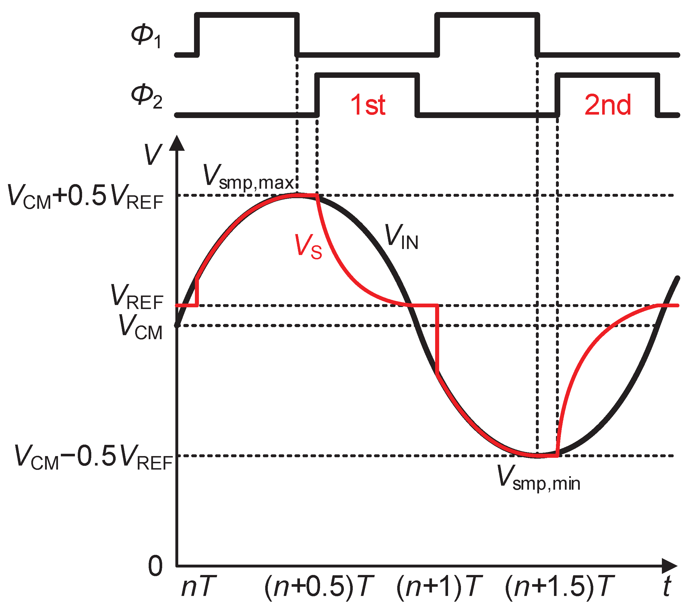
As shown in Figure 2, the input voltage is set to = + 0.5sin(2πt/T). Therefore, the maximum and minimum sampling voltage is ( + 0.5) and (), respectively. is reduced from to during the first settling period, which is a discharge process. On the contrary, is charged from to during the second settling period. A wide pull–push voltage range requires the RVB in Figure 1 to exhibit a strong Class-AB characteristic in high-precision pipelined ADCs.
Figure 2.
Variations of in two periods.
Taking the second settling period as an example in Figure 3, it is clear that the process of the settling can be divided into two parts based on the voltage changing rate. The first part is large signal settling, and 90% of the charging process is completed within in this part. The other 10% of the settling process is finished within in another part, which is called small signal settling. The relationship between the settling time of and the sampling rate of the pipelined ADC is
Consequently, fast settling is critical to pipelined ADCs in high-speed applications.
varies linearly at a defined quiescent operating point during the small signal settling. Therefore, for the convenience of calculation, the small signal settling is considered first. The -domain circuit in small signal settling is depicted in Figure 4, where the RVB is modeled using Thevenin’s theorem. The initial voltage of is set to − (assuming the large signal settling is ideal). The -domain function of can be written as
However, needs to satisfy () − ≤ after the small signal settling. As a result, the time of small signal settling can be calculated as
According to (3), the smaller the of the RVB, the shorter the . Therefore, the RVB with low output resistance is efficient in reducing the settling time of the reference voltage, which is beneficial to realize high-speed pipelined ADCs.
Figure 3.
Details of the second settling period.
Figure 4.
-domain circuit in small signal settling.
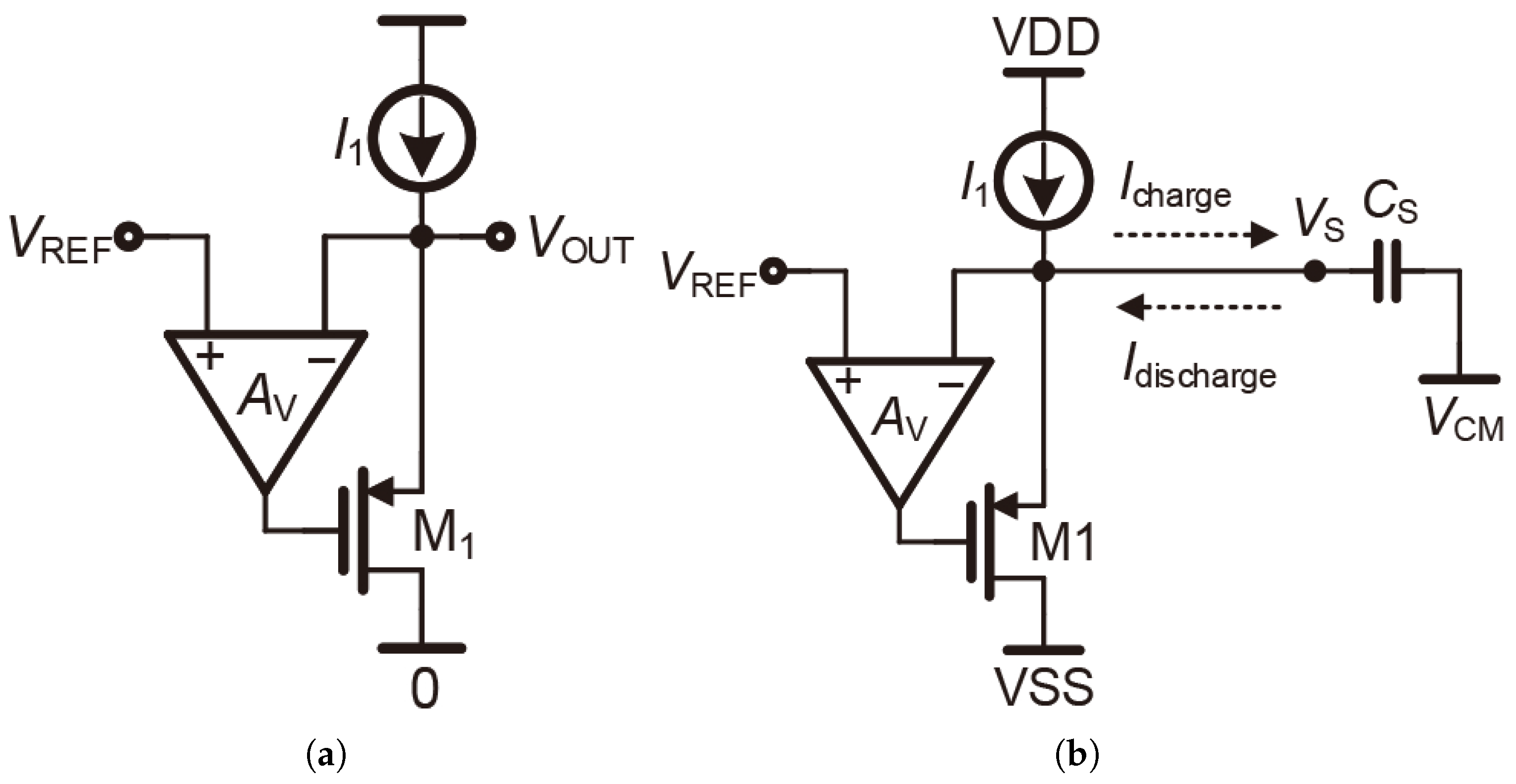
The conventional RVB is mainly designed based on the single-transistor source follower, and its output resistance is about 1/. The source follower with an added amplifier is proposed in Figure 5a, and it is clear that a negative feedback network is formed between M1 and the amplifier to stabilize the output voltage. The output resistance of Figure 5a can be calculated as about 1/(), which is reduced to 1/ of the original source follower. More importantly, a negative feedback is formed by the amplifier with M1, which enables the output voltage to follow the input voltage accurately. Furthermore, Figure 5a is employed as the RVB, as shown in Figure 5b. and correspond to the driving currents of the second and the first large signal settlings in Figure 2, respectively. The time of the two large signal settlings can be derived as
where the and are the driving currents. According to (4), regardless of < 0 or > 0, the RVB is required to generate a large driving current for achieving short . As can be seen in Figure 5b, when < 0, is able to be discharged quickly in large signal settling due to the divergent . However, since the largest is limited to , the of charging is predictably long. Therefore, the RVB in Figure 5a does not possess a Class-AB characteristic, although its output resistance is reduced by the amplifier. As a result, the source follower with an amplifier is not suitable for use as an RVB directly.
Figure 5.
(a) Source follower with an amplifier. (b) Large signal settling.
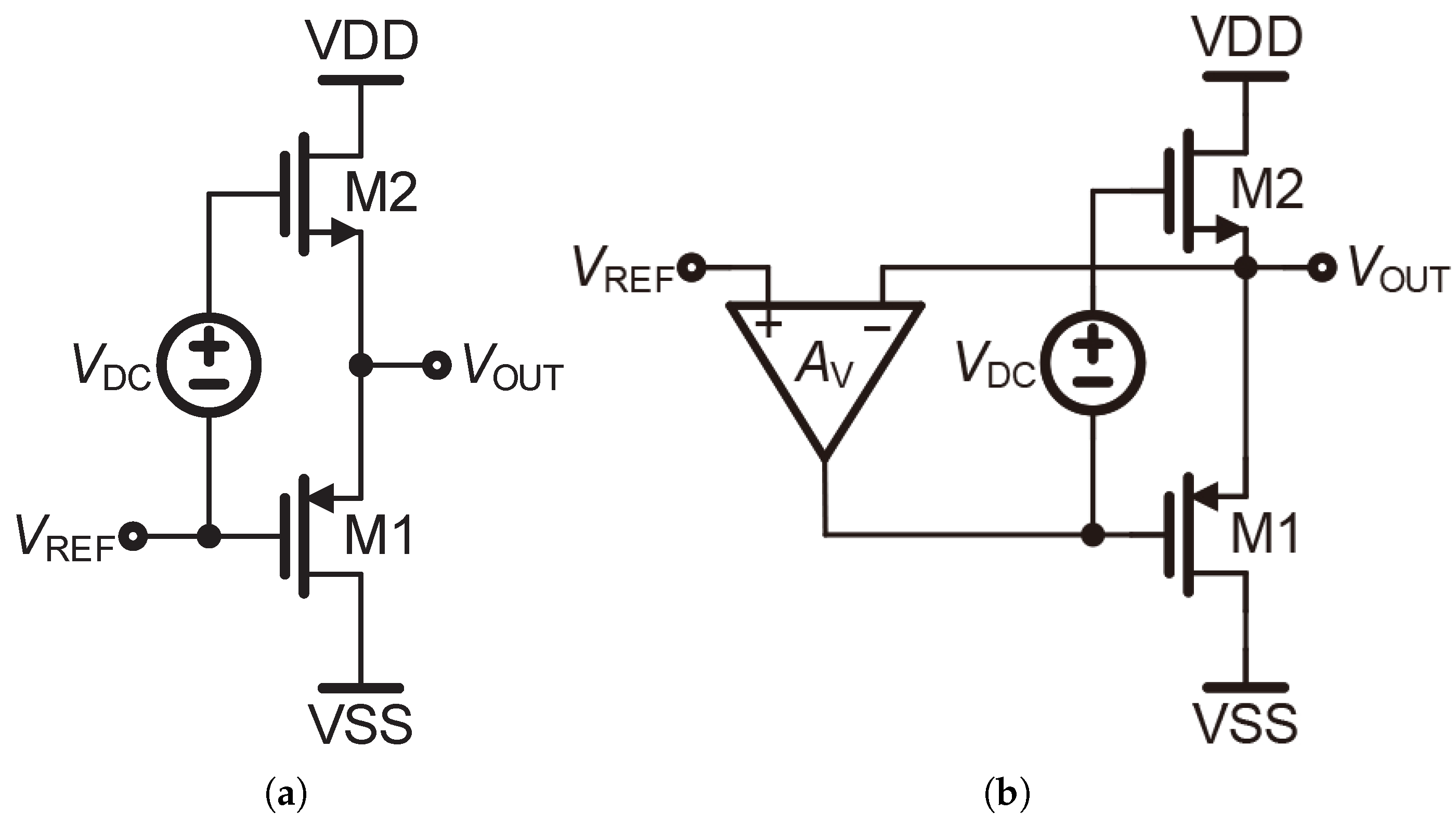
Figure 6a displays the structure of the Class-AB RVB. It can be seen that M1 and M2 directly provide divergent and , respectively. Nonetheless, the output resistance of Figure 5a is about 1/( + ), which limits the speed of the small signal settling. By adding an amplifier to comprise a negative feedback network with M1 and M2 as plotted in Figure 6b, the output resistance is reduced to about 1/().
Figure 6.
(a) Class-AB RVB. (b) Class-AB RVB with a negative feedback network.
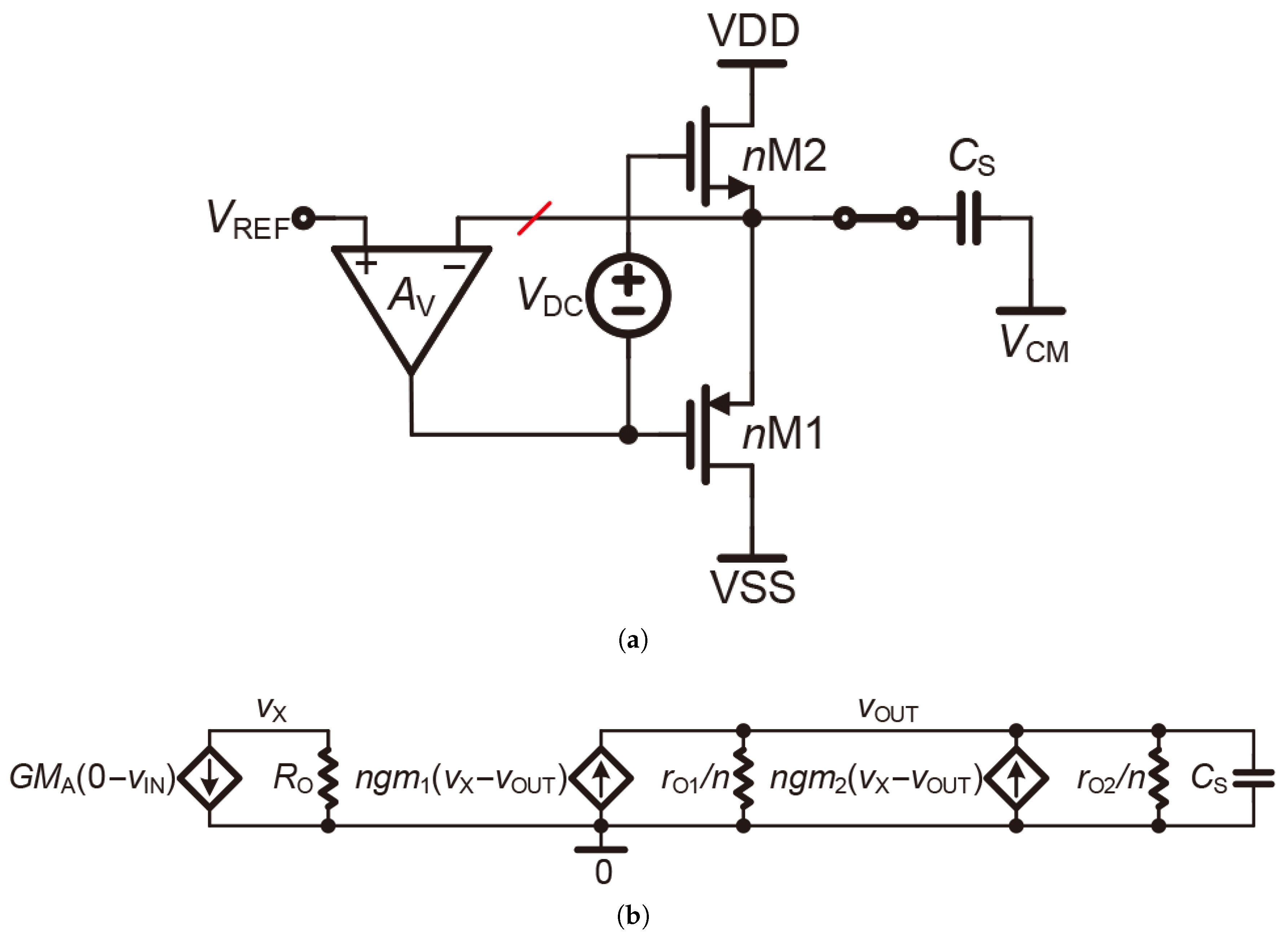
As shown in Figure 7a, the structure of Figure 6b is employed to settle . In the Class-AB type output stage, the numbers of M1 and M2 are set to ( > 1). However, it is obvious that the loop characteristics are influenced by . In this case, the loop stability is worthy of consideration. The loop is broken at the inverting input of the amplifier, and the small signal circuit is displayed in Figure 7b. The amplifier is Norton-equivalent to a parallel combination of a current source and an output resistor. The transfer function can be calculated as
where = ( + ) and = ( // )/n. Equation (5) reveals that a large contributes a low-frequency pole during loop settling, which could extend the small signal settling time. Different from Figure 4, the small signal settling on in Figure 7a is not a simple first-order RC settling model due to the changeable gate voltages of nM1 and nM2. Moreover, the loop needs to be re-established during each settling process, which limits the speed of ADCs. As a result, it is significant to separate from the loop in the Class-AB RVB architecture.
Figure 7.
(a) settling on . (b) Small signal circuit.
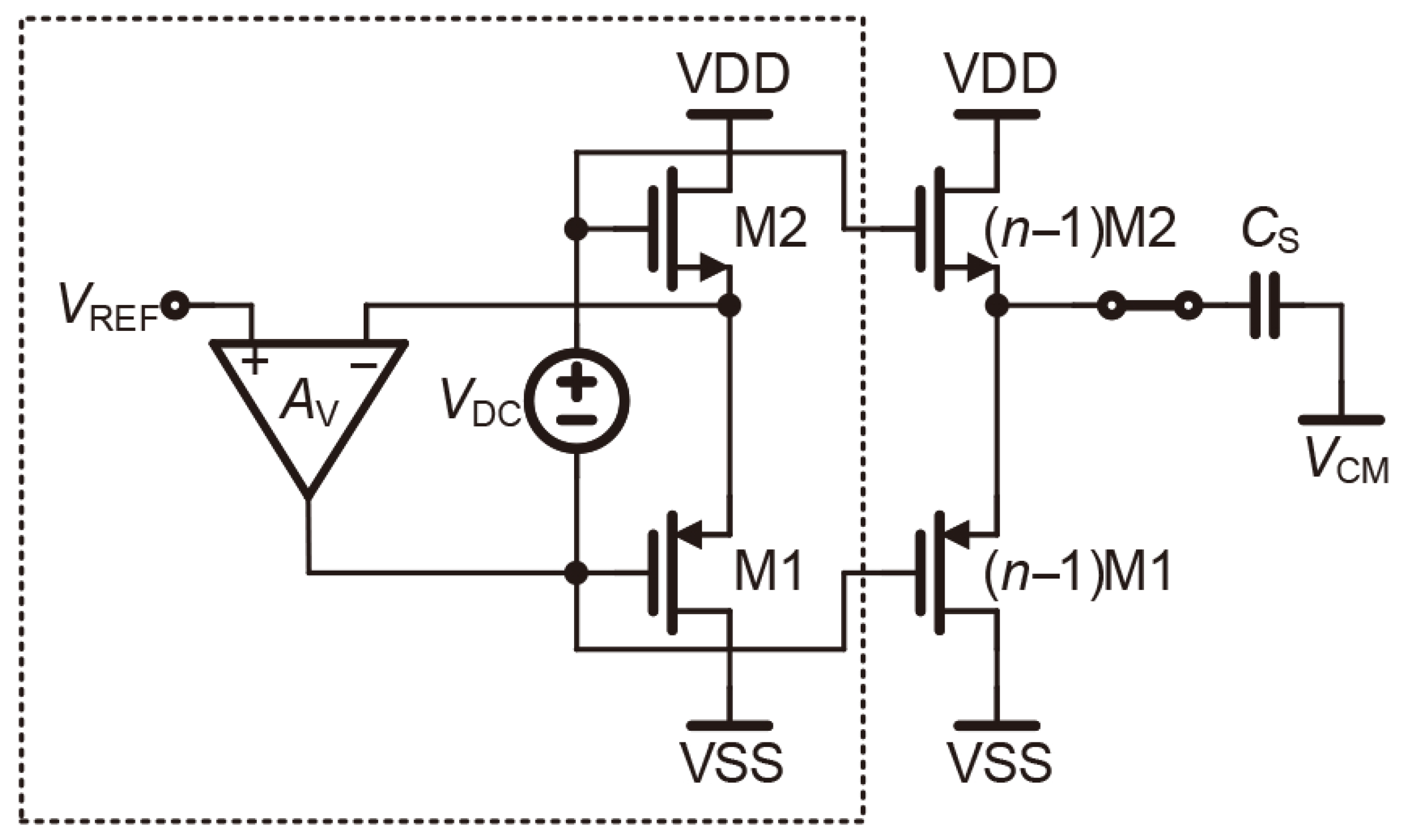
To avoid the loading effect in Figure 7a, the replica source-follower is used to isolate the loop from the large as depicted in Figure 8 [27,28,29,30,31,32]. Thanks to the replica-driving technique, the loop in the dotted box is independent and stable during each settling process, and the open-loop settling only depends on the Class-AB type output stage. Meanwhile, the settling voltage on is precisely mirrored from the negative feedback loop without loading effect. Although the output resistance is not considerably small (1/(n + n)), stable gate voltages of M1 and M2 are more decisive factors in fast small signal settling.
Figure 8.
Class-AB RVB with the replica-driving technique.
As outlined above, the framework in Figure 8 offers two key advantages. First, for different capacitive loads, the driving current can be directly and dynamically supplied by ()M1 and ()M2. This Class-AB feature achieves a superior slew rate of the output stage. Strong driving capability is well-suited for the pipelined ADC applications that demand high-speed performance. On the other hand, the gate voltages of ()M1 and ()M2 are linked to the input voltage by a negative feedback network, which defines the final value of the output reference voltage without the load effect. However, in Figure 8 is an ideal model. As a result, can provide a voltage drop for the DC bias while transmitting AC small signals in the negative feedback network. In practical circuits, implementing the negative feedback loops for both M1 and M2 requires more elaborate calculations and settings for the RVB’s quiescent operating point.
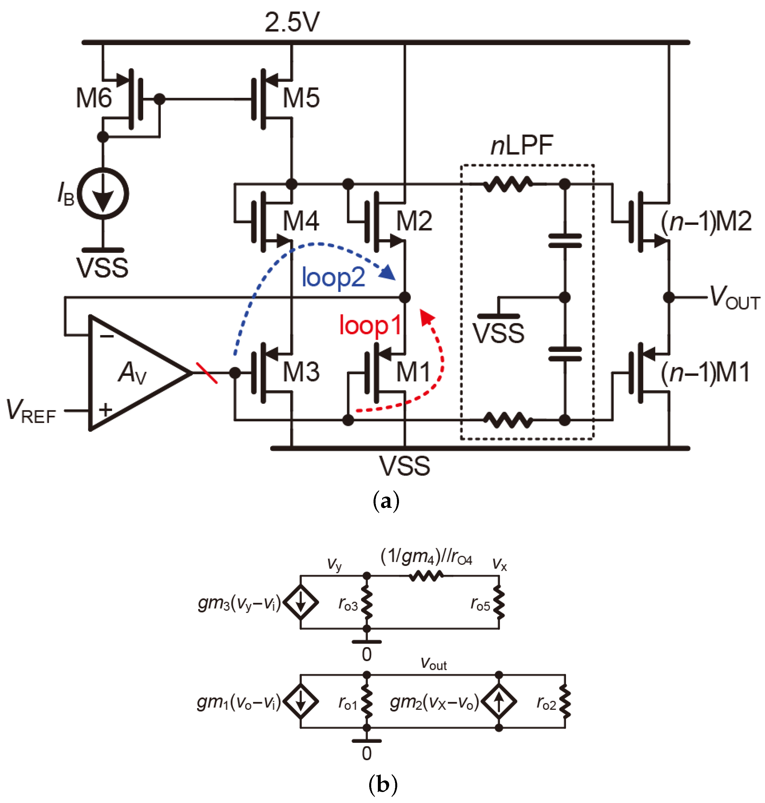
Based on the design signal of negative feedback and Class-AB output stage, ref. [21] presents a Class-AB RVB for a 12-bit 250 MS/s pipelined SAR ADC, as shown in Figure 9a. There are kinds of capacitors in each sub-ADC, and MDAC needs to be charged or discharged by the RVB. In order to obtain stable gate voltages of ()M1 and ()M2 and reduce the noise interference, the low-pass filters (LPFs) are added in each Class-AB output stage. In contrast to the clear circuit topology and noise cancellation of the output stage, the analysis of the bias circuit of M1 and M2 is even more critical. In Figure 9a, M3 and M4 are equal to M1 and M2, respectively. The negative feedback loop1 (red) is formed by M1 and the operational amplifier: increases → increases → increases → () decreases. M3, M4, M5, M6 and are designed to generate the bias voltage of M2. Meanwhile, the negative feedback loop2 (blue) is also formed: increases → increases → increases → increases → increases → () decreases. It is clear that loop1 and loop2 interact with each other. In order to analyze the negative feedback network in the bias circuit more accurately, a loop-breaking process is performed at the output of the operational amplifier. The small signal diagram of the feedback network is shown in Figure 9b. The output and negative input terminals of the operational amplifier are defined as and for obtaining the feedback factor :
The approximation that >> 1/gm yields the result that β ≈ 1. With the ideal amplifier assumption ( = +∞), the transfer function of Figure 9a can be derived as:
Based on the calculation results and the circuit configuration, as an RVB, Figure 9a achieves output-to-input tracking while maintaining great Class-AB characteristics. However, to generate a reference voltage of 1.2 V, the circuit of Figure 9a operates with a 2.5 V supply voltage, which results in considerable quiescent power consumption (the overall power consumption of the pipelined SAR ADC is 31.5 mW). Moreover, using both thick-oxide NMOS transistors and thin-oxide PMOS transistors also increases the design complexity of the RVB.
Figure 9.
(a) Class-AB RVB of [21]. (b) Small signal circuit of the loop.
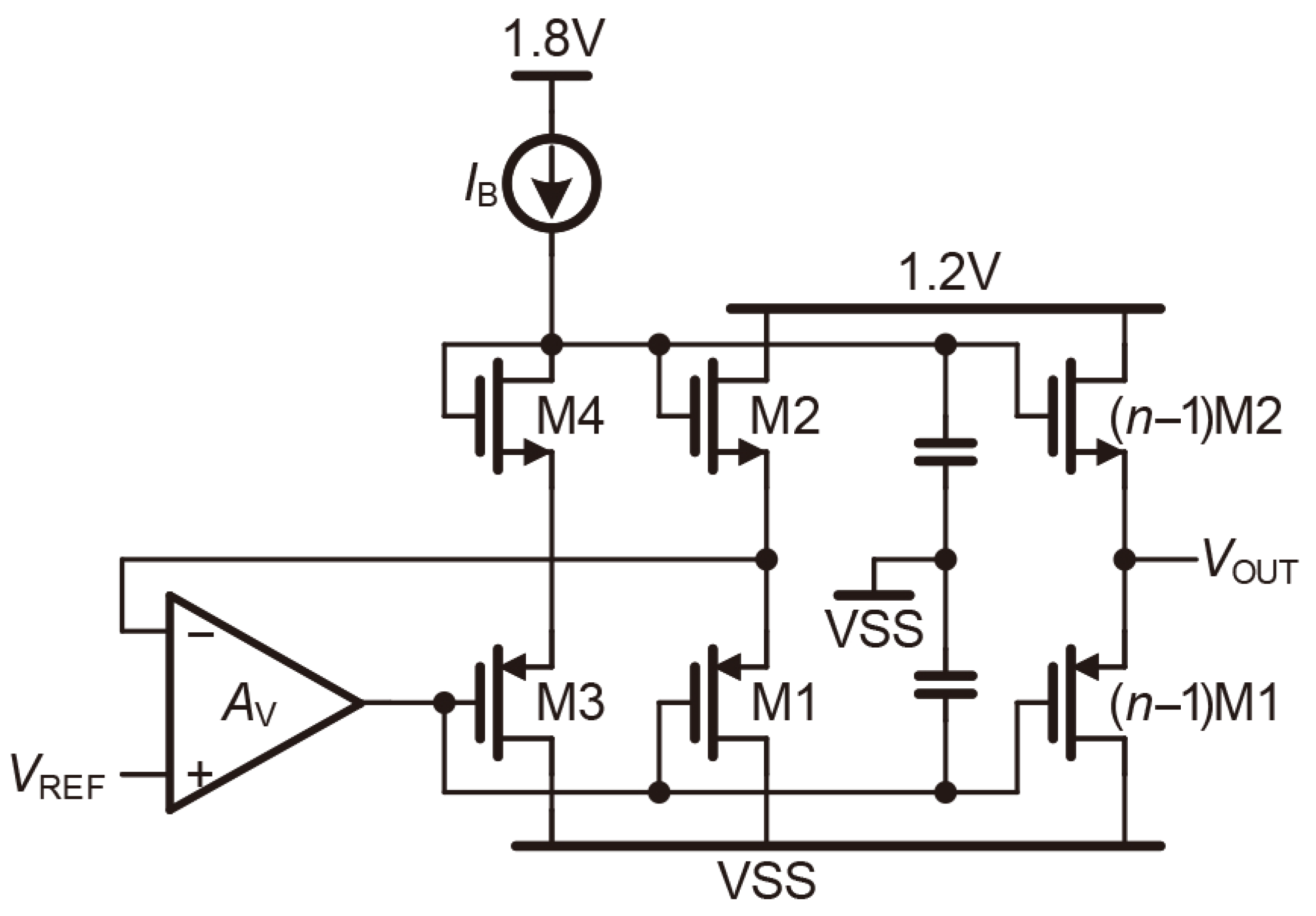
For overcoming the power consumption issue of Figure 9a, a low-power Class-AB RVB is presented and applied in a 12-bit 1 GS/s pipelined TI-SAR ADC [22], as shown in Figure 10. The bias circuit provides the gate voltages of M1(()M1) and M2(()M2) with a supply voltage of 1.8 V. Moreover, since the input swing of the ADC is 1 V, the output stage of the RVB is required to provide a stable 1 V reference voltage with a 1.2 V supply voltage. By separating the supply voltages of the bias circuit and the output stage, the power consumption of Figure 10 is reduced to only 3.7 mW.
Figure 10.
Class-AB RVB of [22].
It is worth noting that in Figure 10 is equivalent to M5 in Figure 9a. As a result, the negative feedback networks of the bias circuits in the two RVBs are identical. In fact, this type of RVB circuit structure still has certain drawbacks. Firstly, a branch consisting of (M5), M3, and M4 is added to generate a DC bias voltage for M2. However, M3 and M4 are equal to M1 and M2, but is independent of . A large voltage difference between the source terminals of M4 and M2 will decrease the matching performance of the two branches in the bias circuit. Taking Figure 10 as an example, the two branches are greatly matched only if the voltage drop of is 0.6 V. Secondly, ()M1 and ()M2 are supposed to have comparable impacts on , but in the two proposed RVBs, the small signal feedback paths of the gate voltage of ()M2 are more complex than those of ()M1. Finally, ()M2 are directly connected to the supply voltage, and the fluctuations of the supply voltage would reduce the stability of the . A deteriorated PSRR of the RVB leads to a lower signal-to-noise ratio (SNR) and fewer effective number of bits (ENOB) of the corresponding high-precision ADCs.
3. The Proposed RVB
3.1. Circuit Architecture
In Figure 11, the current-driven proposed RVB generates different by adjusting the input current dynamically ( = ). not only determines the output voltage of this RVB but also generates the bias voltages for M4. The current mirror transistors in output stage are ()× those in the loop. Considering the large capacitors of high-precision MDACs, it is worth noting that the driving current of the output stage circuit is amplified by a factor of . is used to minimize high-frequency noise at the output stage, which is beneficial to the generation of an accurate reference voltage. In the output stage, the amplifier not only forms a negative feedback loop with M5, but also constitutes the other negative feedback loop with M4 by . Compared with the Class-AB type RVBs proposed by [21,22], the RVB in Figure 11 exhibits superior matching performance due to the equivalent source voltages of M2 and M4. ()M3 is used to mitigate the impact of supply voltage fluctuations on the output voltage.
Figure 11.
The proposed RVB circuit.
3.2. Loop Stability
The loop stability of the proposed RVB needs to be analyzed and verified due to the two additional feedback loops provided by . Figure 12 can be obtained by breaking the loop at the input of the amplifier, and the amplifier is Norton-equivalent to a parallel combination of a current source and an output resistor. The equivalent impedance within the dashed box can be written as
can be described by
where and are the equivalent differential inputs after breaking the loop. is the equivalent transconductance of the simplified operational amplifier. Furthermore, the differential feedback voltages can be obtained as follows:
Considering (1/) << , 1/ () = 1/ () and 1/ () = 1/ (), the loop gain can be calculated as
In (11), () represents the complex frequency-domain term, which determines the frequency response of the loop. It can be seen from the denominator and numerator of () that the loop contributes two poles and two zeros. In general, a stable RVB requires the output resistance () of the high-gain cascode amplifier to realize = , which indicates that + 1/ + ≈ ( >> 1/ ≈ ). As a result, the denominator of () can be rewritten as
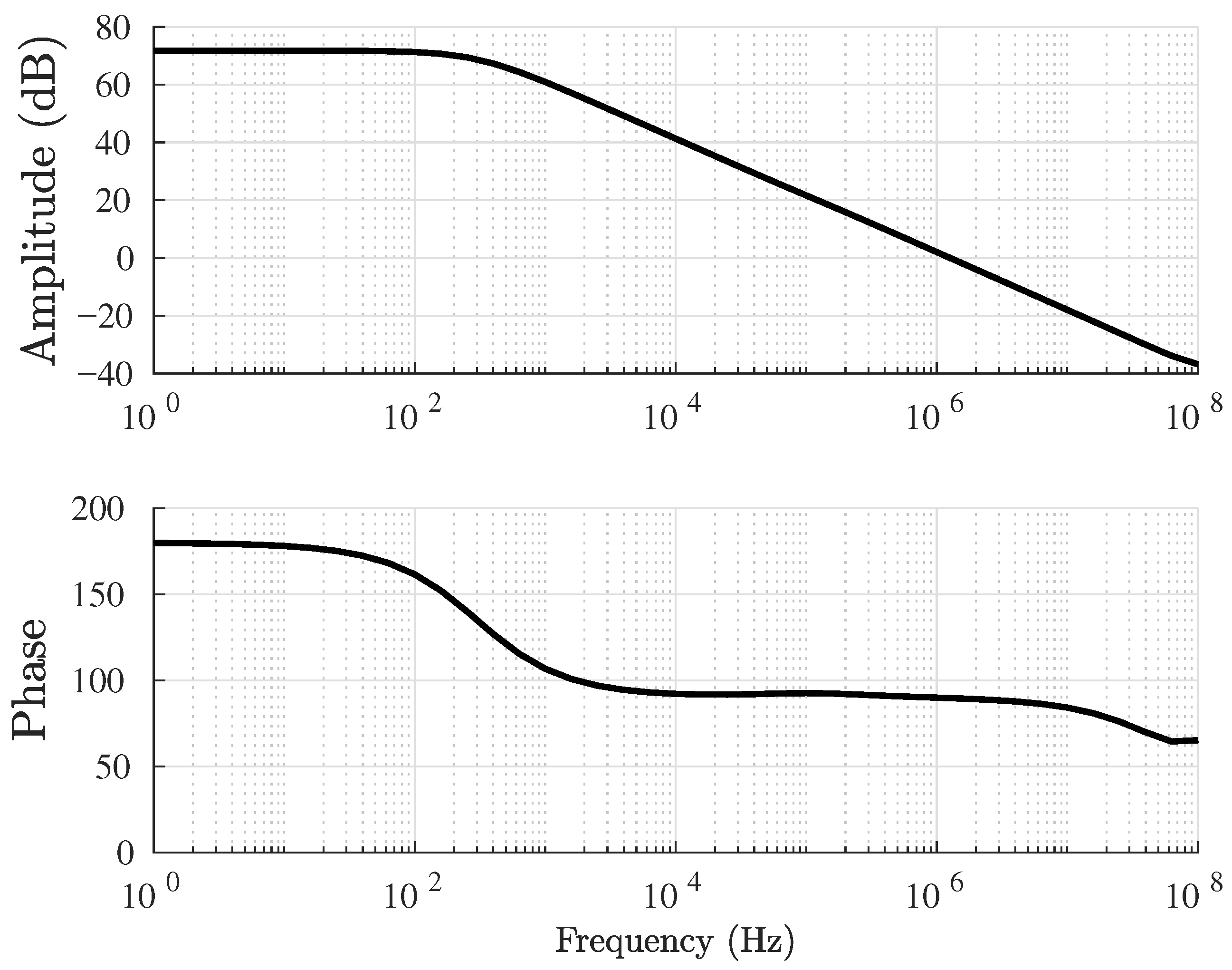
As calculated in (12), the dominant pole is determined by the output resistance of the amplifier () and the gate-to-gate capacitor (). and 1/ are considered as around 0.1 GΩ and 0.1 kΩ. , , and are set to 10 pF, 30 pF, and 10 kΩ, respectively. The frequency of can be estimated at kilohertz. and two zeros are located in the high-frequency region around the gigahertz level according to (12) and (11).
Figure 12.
The simplified RVB for analyzing loop stability.
The simulation results in Figure 13 present the magnitude and phase plot of the loop gain. As expected, the position of the dominant pole is around 0.3 kHz, and the loop approximates a single-pole system in the frequency range of 100 MHz. In addition, the sufficient phase margin is significant for the stability of the loop, and it is fortunate that the phase shift is only almost 90° within the gain crossover frequency.
Figure 13.
Bode plot of the loop gain.
4. Simulation Results
4.1. Driving Capability
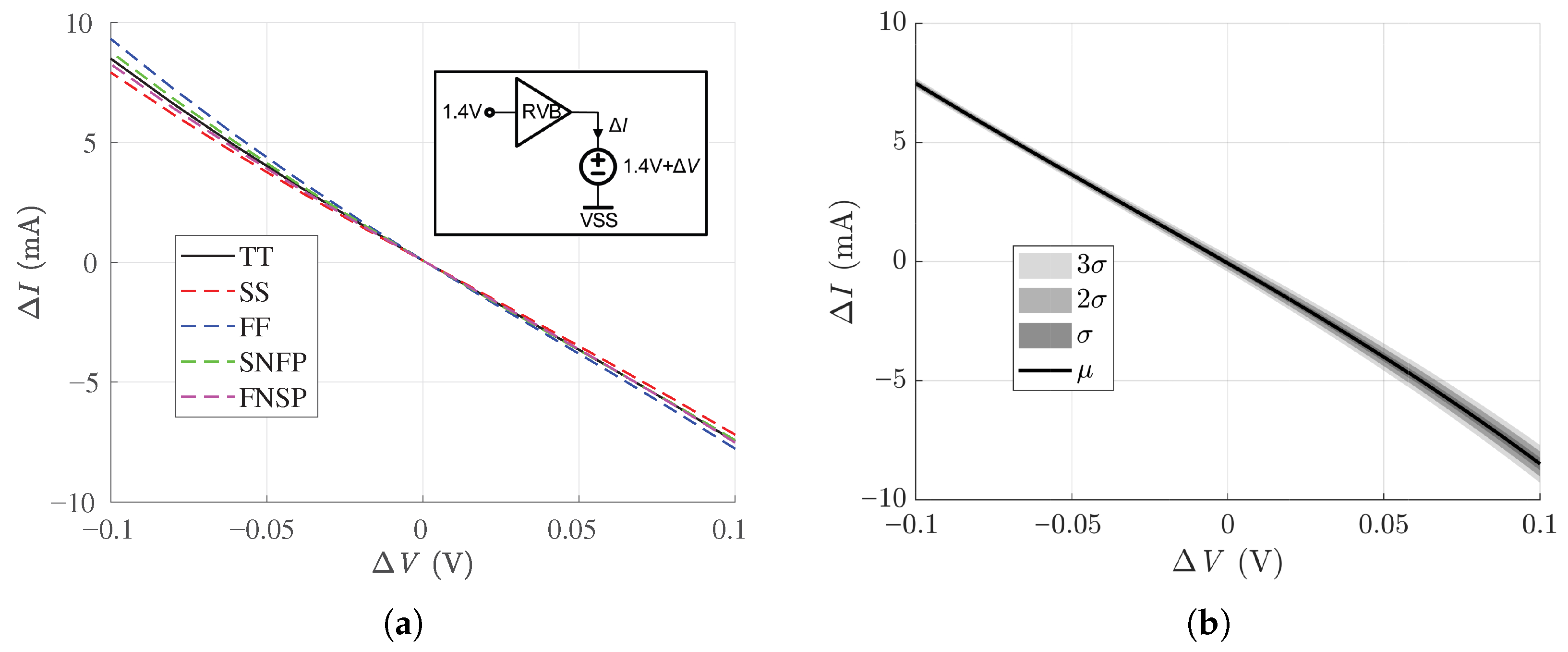
The driving current of the output stage under the error voltage can intuitively reflect the driving capability and dynamic response speed of RVBs in pipelined ADCs. As can be seen from Figure 14a, is set to 1.4 V, and the output port of the proposed RVB is connected to a 1.4 V + DC voltage source. The magnitude of reflects the driving capability of the proposed RVB. To ensure that the proposed RVB drives the DAC array steadily under different manufacturing variations, the simulation results have been obtained under the following PVT process corners: Typical (TT), Slow (SS), Fast (FF), Slow-NMOS-Fast-PMOS (SNFP), and Fast-NMOS-Slow-PMOS (FNSP). Class-AB type milliampere-level is observed, which suggests that the proposed RVB is able to deal with both positive and negative evenly. Figure 14b shows 1000-run process and mismatch Monte Carlo (MC) results, which are employed to obtain the mean value () and the standard deviation (). Although increases with the rise in , the proposed RVB still behaves with high robustness during variation.
Figure 14.
as a function of : (a) Corners of PVT; (b) 1000-run Monte Carlo.
The output is observed by sweeping the load current source with a wide variation range in PVT corners simulation (Figure 15a) and MC simulation (Figure 15b). The output voltage error is expressed as: = ()/1.4. In the output stage of Figure 11, ()M4 and ()M5 turn off when reaches ∼−30 mA and ∼18 mA, respectively. However, due to the Class-AB characteristics of the proposed RVB, does not increase abruptly after ()M4 and ()M5 turning off. Moreover, even the worst corner (FF process corner) has only 7.8% and −8.5% of when the reaches −10 mA and 10 mA as depicted in Figure 15a. Figure 15b still demonstrates the great robustness of the proposed RVB and smaller in the charging process.
Figure 15.
as a function of : (a) corners of PVT; (b) 1000-run Monte Carlo.
4.2. Transient Response
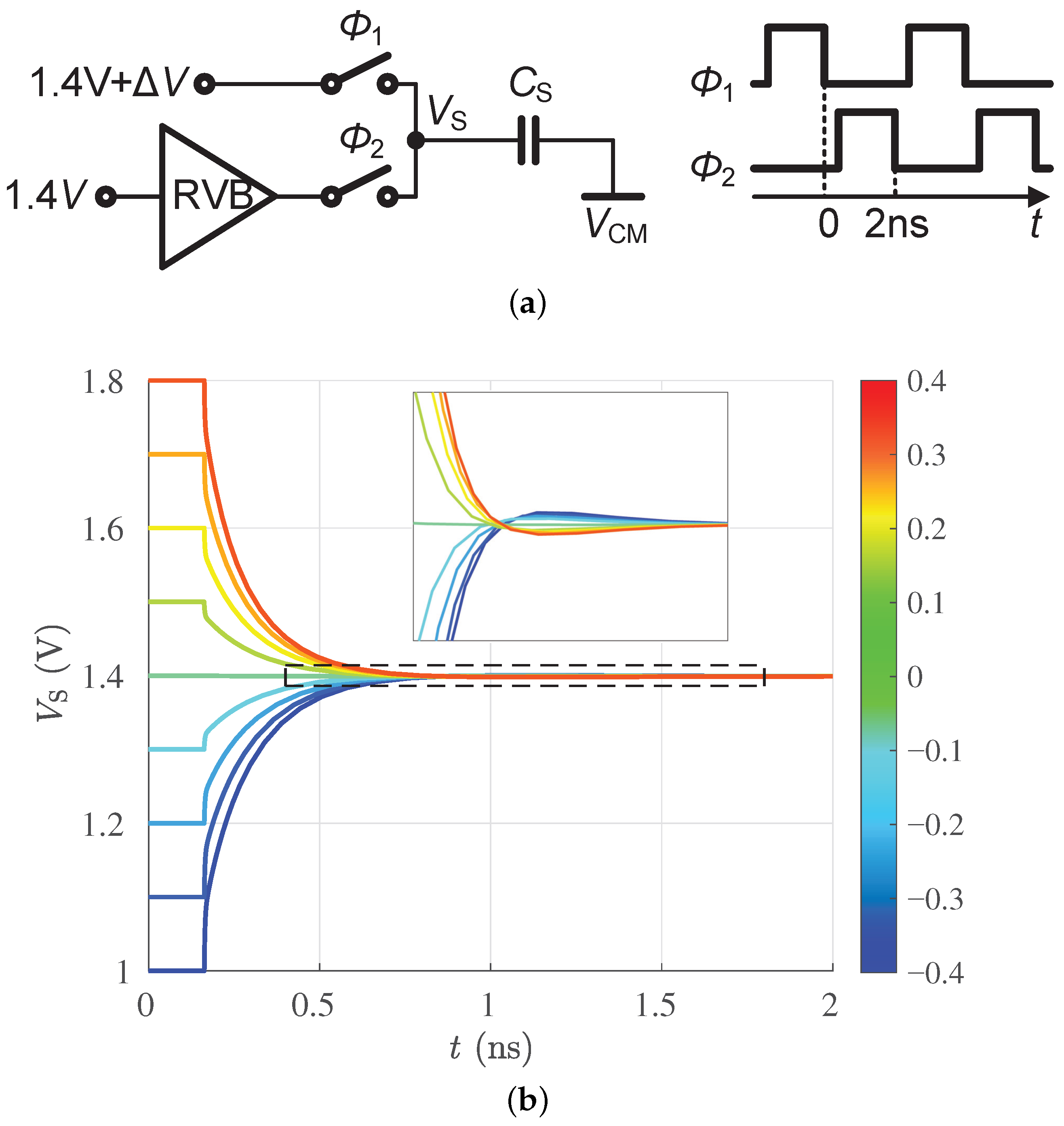
The proposed RVB is required to restore the voltage of sampling capacitors from the input voltage to the reference voltage accurately within an ultra-short time in high-speed pipelined ADCs. For evaluating the reference voltage settling performance of the proposed RVB in pipelined ADCs, the simulated circuit of transient response and the timing diagram are presented in Figure 16a. The sampling capacitance and the reference voltage are set to 9 pF and 1.4 V, respectively. is the voltage difference between the sampled input voltage (( = 0)) and 1.4 V, which is required to be overcome by the proposed RVB at = 0 to 2 ns. The simulation results in the TT process corner are illustrated in Figure 16b; the larger the , the greater the difficulty in settling, and the longer the settling time. Due to the Class-AB characteristic of the proposed RVB, it is clear that (−0.4 V to 0.4 V) is settled evenly and effectively within 1 ns. The details in the dotted box are magnified. Despite the impact of non-ideal factors (e.g., parasitic capacitance) on overshoot, the small signal settling behavior broadly follows first-order RC settling (as shown in Figure 4).
Figure 16.
Transient response simulation: (a) circuit and (b) result.
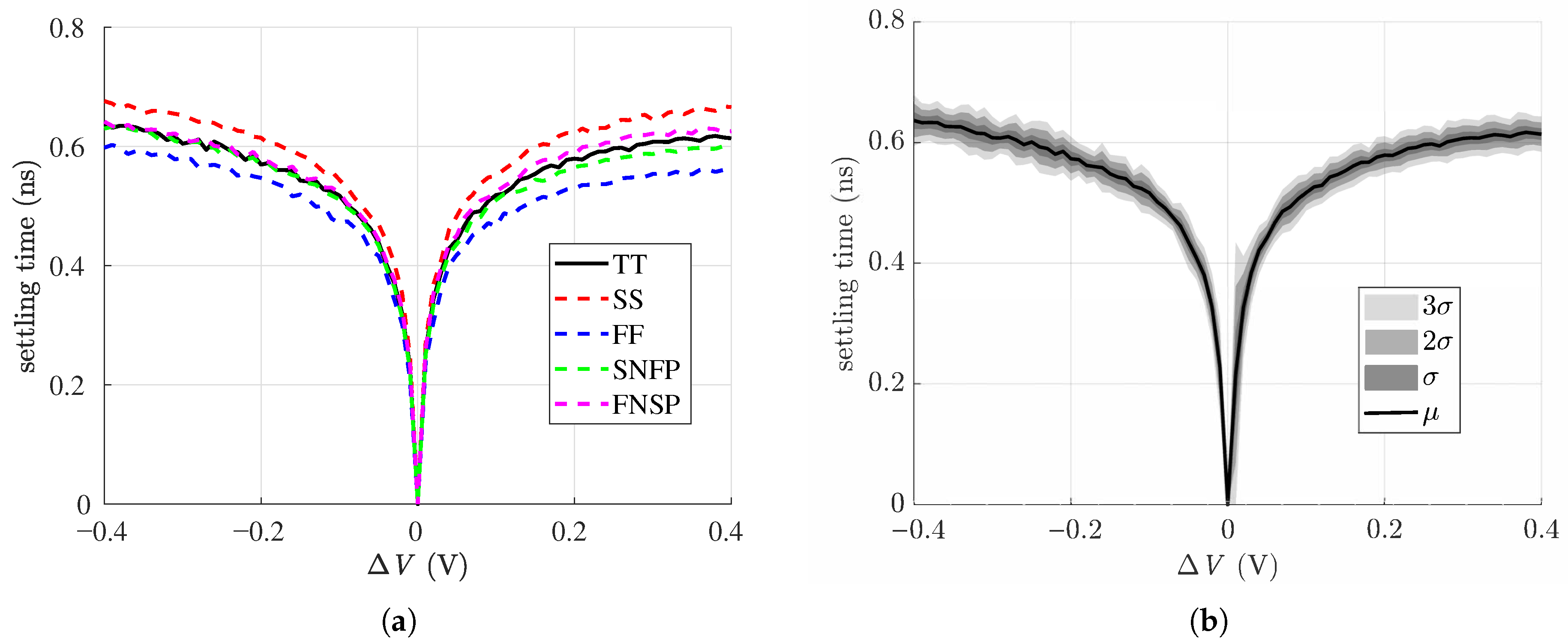
According to Figure 16, in five process corners, Figure 17 shows the required settling times of the proposed RVB when the final settling error is constrained within 1 ( is set to /210). In Figure 17a, it can be clearly observed that the proposed RVB buffers the desired reference voltage () within 0.68 ns (SS process corner) under the condition of (−0.4 V to 0.4 V). For a pipelined ADC, the settling time of the reference should not exceed half of the conversion time. In other words, the proposed RVB is prospective to be employed in the pipelined ADC with the precision of 10-bit and the speed of 735 MS/s. Figure 17b presents the expected and small of settling time, which indicates the stability of the proposed RVB in high-speed and high-precision pipelined ADC applications.
Figure 17.
Required settling time: (a) corners of PVT; (b) 1000-run Monte Carlo.
4.3. Power Supply and Temperature Sensitivities
PSRR quantifies a circuit’s ability to suppress power supply fluctuations, which is a core indicator for analog circuit design. As illustrated in Table 1, PSRR is simulated as a function of frequency, and obviously, PSRR is stable in different process corners. The robustness of the proposed RVB is verified again by 1000-run MC simulation results of PSRR. Owing to the ()M3 displayed in Figure 11, the gain of the power supply noise is attenuated. In the different process corners, the PSRR of the proposed RVB is equal to ∼129 dB at 1 Hz, ∼107 dB at 1 kHz, and ∼60 dB at 1 MHz. Therefore, it can be expected that the proposed RVB has sufficient attenuation for the injected noise from the power supply voltage.
Table 1.
PSRR performance at different frequencies.
The input voltage of the proposed RVB is still set to 1.4 V ( = 1.4 V in Figure 11), and the temperature sensitivity of its output voltage () is displayed in Figure 18. The temperature coefficient (TC) of five process corners can be obtained by Figure 18a: TCTT ≈ TCSS ≈ TCFF ≈ TCSF ≈ TCFS ≈ 363 ppm/°C. High temperature sensitivity of R results in the large TC of . However, as shown in Figure 18b, the Monte Carlo simulation results prove that the proposed RVB itself is stable and robust.
Figure 18.
as a function of temperature: (a) Corners of PVT; (b) 1000-run Monte Carlo.
5. Conclusions
In this work, a novel Class-AB RVB is proposed. The theoretical derivation demonstrates the loop stability of the proposed RVB. The simulation results indicate that the proposed RVB achieves not only wonderful driving capability but also excellent settling accuracy and speed. Moreover, high PSRR demonstrates that the output voltage of the proposed RVB is insensitive to the variations in the supply voltage.
Table 2 summarizes the performance of the proposed RVB. In comparison with the previous RVBs, although the power consumption of the proposed RVB increases inevitably owing to the replica-driving output stage with a large current, it is still only 4.5 mW. Fortunately, the proposed RVB achieves not only higher PSRR but also more outstanding driving capability for large capacitive loads. These properties indicate that the proposed RVB is feasible to be applied in high-speed and high-precision pipelined ADCs.
Table 2.
Performance summary and comparison.
Author Contributions
Data curation, L.Z.; Formal analysis, L.Z. and M.W.; Methodology, L.Z.; Supervision, R.Y.; Validation, L.Z. and Y.G.; Software, L.Z. and Y.Z.; Project administration, Z.T.; Writing—original draft, L.Z.; Writing—review and editing, L.Z. and M.W. All authors have read and agreed to the published version of the manuscript.
Funding
This research received no external funding.
Data Availability Statement
The data used in this study can be requested from the corresponding author.
Acknowledgments
The authors thank the Inbisen Semiconductor Co., Ltd. for the financial and technical support. Honour the memory of Senior Brother Liang Zou.
Conflicts of Interest
The authors declare no conflicts of interest.
References
- Kurose, D.; Ito, T.; Ueno, T.; Yamaji, T.; Itakura, T. 55-mW 200-MSPS 10-bit pipeline ADCs for wireless receivers. IEEE J. Solid-State Circuits 2006, 41, 1589–1595. [Google Scholar] [CrossRef]
- Shibata, H. Continuous-Time Pipelined ADC: A Breed of Continuous-Time ADCs for Wideband Data Conversion. IEEE Open J. Solid-State Circuits Soc. 2023, 3, 162–173. [Google Scholar] [CrossRef]
- Dhiman, S.; Shrimali, H. An MDAC-Less Pipelined ADC for AI-Powered Medical Imaging Applications. IEEE Sens. J. 2024, 24, 39182–39194. [Google Scholar] [CrossRef]
- He, J.; Hu, J.; Liu, S.; Feng, S.; Wang, D. A 12-bit 100-MS/s Pipeline SAR ADC for Professional Medical Field. In Proceedings of the 6th International Conference on Electrical, Electronic Information and Communication Engineering (EEICE), Shenzhen, China, 18–20 April 2025; pp. 487–491. [Google Scholar]
- Kim, K.; Yu, W.; Cho, S. A 9 bit, 1.12 ps Resolution 2.5 b/Stage Pipelined Time-to-Digital Converter in 65 nm CMOS Using Time-Register. IEEE J. Solid-State Circuits 2014, 49, 1007–1016. [Google Scholar] [CrossRef]
- Maatta, K.; Kostamovaara, J. A high-precision time-to-digital converter for pulsed time-of-flight laser radar applications. IEEE Trans. Instrum. Meas. 1998, 47, 521–536. [Google Scholar] [CrossRef]
- Verbruggen, B.; Craninckx, J.; Kuijk, M.; Wambacq, P.; Van der Plas, G. A 2.6 mW 6 bit 2.2 GS/s Fully Dynamic Pipeline ADC in 40 nm Digital CMOS. IEEE J. Solid-State Circuits 2010, 45, 2080–2090. [Google Scholar] [CrossRef]
- Zhu, Y.; Liu, T.; Kaile, S.K.; Kiran, S.; Yi, I.-M.; Liu, R.; Diaz, J.C.G.; Hoyos, S.; Palermo, S. A 38-GS/s 7-bit Pipelined-SAR ADC with Speed-Enhanced Bootstrapped Switch and Output Level Shifting Technique in 22-nm FinFET. IEEE J. Solid-State Circuits 2023, 58, 2300–2313. [Google Scholar] [CrossRef]
- Liu, J.; Hassanpourghadi, M.; Chen, M.S.-W. A 10-GS/s 8-bit 2850-μm2 Two-Step Time-Domain ADC with Speed and Efficiency Enhanced by the Delay-Tracking Pipelined-SAR TDC. IEEE J. Solid-State Circuits 2022, 57, 3757–3767. [Google Scholar] [CrossRef]
- Yu, L.; Miyahara, M.; Matsuzawa, A. A 9-bit 1.8 GS/s 44 mW Pipelined ADC Using Linearized Open-Loop Amplifiers. IEEE J. Solid-State Circuits 2016, 51, 2210–2221. [Google Scholar] [CrossRef]
- Hao, J.; Zhang, M.; Liu, Z.; Zhang, Y.; Liu, S.; Zhu, Z.; Zhu, Y.; Martins, R.P.; Chan, C.-H. An Intrinsically PVT Robust 10-bit 2.6-GS/s Dynamic Pipelined ADC with Dual-Path Time-Assisted Residue Generation Schem. IEEE J. Solid-State Circuits 2025, 60, 2545–2557. [Google Scholar] [CrossRef]
- Zhang, Z.; Hu, Y.; Lang, L.; Dong, Y. A 16 Bit 125 MS/s Pipelined Analog-to-Digital Converter with a Digital Foreground Calibration Based on Capacitor Reuse. Electronics 2024, 13, 1474. [Google Scholar] [CrossRef]
- Wu, J.; Xu, H.; Cao, X.; Liu, T. A 16-Bit 120 MS/s Pipelined ADC Using a Multi-Level Dither Technique. Electronics 2022, 11, 3979. [Google Scholar] [CrossRef]
- Wu, Y.; Ye, F.; Ren, J. A Calibration-Free, 16-Channel, 50-MS/s, 14-Bit, Pipelined-SAR ADC with Reference/Op-Amp Sharing and Optimized Stage Resolution Distribution. Electronics 2022, 11, 749. [Google Scholar] [CrossRef]
- Zhou, X.; He, W.; Su, C.; Liu, T.; Fu, D.; Li, Q. A Low Power 16-bit 125MS/s Pipeline ADC with 100dB SFDR. In Proceedings of the IEEE International Symposium on Circuits and Systems (ISCAS), Singapore, 19–22 May 2024; pp. 1–5. [Google Scholar]
- Cao, H.; Yu, Z.; Deng, H.; Li, P. A reference voltage source and its output buffer for pipeline ADC. In Proceedings of the International Conference on Anti-Counterfeiting, Security and Identification (ASID), Macao, China, 1–3 December 2014; pp. 1–5. [Google Scholar]
- Harikumar, P.; Angelov, P.; Hägglund, R. Design of a reference voltage buffer for a 10-bit 1-MS/s SAR ADC. In Proceedings of the 21st International Conference Mixed Design of Integrated Circuits and Systems (MIXDES), Lublin, Poland, 19–21 June 2014; pp. 185–188. [Google Scholar]
- Carvajal, R.; Ramirez-Angulo, J.; Lopez-Martin, A.; Torralba, A.; Galan, J.; Carlosena, A. The flipped voltage follower: A useful cell for low-voltage low-power circuit design. IEEE Trans. Circuits Syst. I Regul. Pap. 2005, 52, 1276–1291. [Google Scholar] [CrossRef]
- Gagliardi, F.; Catania, A.; Piotto, M.; Bruschi, P.; Dei, M. Parallel Slew-Rate Enhancer with Current-Recycling Core for Switched-Capacitors Circuits. IEEE Trans. Circuits Syst. II Express Briefs 2024, 71, 4814–4818. [Google Scholar] [CrossRef]
- Kapusta, R.; Shinozaki, H.; Ibaragi, E.; Ni, K.; Wang, R.; Sayuk, M.; Singer, L.; Nakamura, K. A 4-channel 20-to300 Mpixel/s analog front-end with sampled thermal noise below kT/C for digital SLR cameras. In Proceedings of the IEEE International Solid-State Circuits Conference—Digest of Technical Papers, San Francisco, CA, USA, 8–12 February 2009; pp. 42–43. [Google Scholar]
- Zhou, Y.; Xu, B.; Chiu, Y. A 12-b 1-GS/s 31.5-mW Time-Interleaved SAR ADC with Analog HPF-Assisted Skew Calibration and Randomly Sampling Reference ADC. IEEE J. Solid-State Circuits 2019, 54, 2207–2218. [Google Scholar] [CrossRef]
- Zhan, M.; Jie, L.; Zhong, Y.; Sun, N. A 10-mW 10-ENoB 1-GS/s Ring-Amp-Based Pipelined TI-SAR ADC with Split MDAC and Switched Reference Decoupling Capacitor. IEEE J. Solid-State Circuits 2023, 58, 3576–3585. [Google Scholar] [CrossRef]
- Kim, I.; Qin, Y. A Fully Integrated FVF Based Low-Noise Voltage Buffer for ADC Reference. In Proceedings of the IEEE 17th International Conference on Solid-State Integrated Circuit Technology (ICSICT), Zhuhai, China, 22–25 October 2024; pp. 1–3. [Google Scholar]
- Park, S.; Son, S.; Chung, W. A rail-to-rail unity gain buffer amplifier for low-cost high resolution TFT LCD panels. IEEE Trans. Consum. Electron. 2009, 55, 2190–2194. [Google Scholar] [CrossRef]
- Yu, Z.; Zhou, J. A 12-bit 1 MS/s SAR ADC with Buffers. In Proceedings of the IEEE 17th International Conference on Anti-counterfeiting, Security, and Identification (ASID), Xiamen, China, 1–3 December 2023; pp. 131–134. [Google Scholar]
- He, W.; Ye, F.; Ren, J. A Fast Response Reference Voltage Buffer for 12b 200 MS/s SAR ADC. In Proceedings of the IEEE 63rd International Midwest Symposium on Circuits and Systems (MWSCAS), Virtual, 9–12 August 2020; pp. 1–4. [Google Scholar]
- Yin, Q.; Bai, C. A CMOS Reference Voltage Buffer Designed for Near-rail Voltage. In Proceedings of the IEEE 5th International Conference on Integrated Circuits and Microsystems (ICICM), Nanjing, China, 23–25 October 2020; pp. 173–176. [Google Scholar]
- Seo, M.; Jin, D.; Kim, Y.; Kim, J.; Ryu, S. A Single-Supply CDAC-Based Buffer-Embedding SAR ADC with Skip-Reset Scheme Having Inherent Chopping Capability. IEEE J. Solid-State Circuits 2020, 55, 2660–2669. [Google Scholar] [CrossRef]
- Liang, Y.; Ding, R.; Zhu, Z. A 9.1ENOB 200 MS/s Asynchronous SAR ADC with Hybrid Single-Ended/Differential DAC in 55-nm CMOS for Image Sensing Signals. IEEE Sens. J. 2018, 18, 7130–7140. [Google Scholar] [CrossRef]
- He, W.; Li, Z.; Ye, F.; Ren, J. A Low Power Reference Voltage Buffer and High Density Unit capacitor in a 12b 200 MS/s SAR ADC. In Proceedings of the IEEE Asia Pacific Conference on Circuits and Systems (APCCAS), Ha Long, Vietnam, 8–10 December 2020; pp. 82–85. [Google Scholar]
- Li, W.; Li, F.; Yang, C.; Li, M.; Wang, Z. A power-efficient reference buffer with wide swing for switched-capacitor ADC. Microelectron. J. 2015, 46, 410–414. [Google Scholar] [CrossRef]
- Lee, C.-K.; Kim, W.; Kang, H.; Ryu, S.-T. A Replica-Driving Technique for High Performance SC Circuits and Pipelined ADC Design. IEEE Trans. Circuits Syst. II Express Briefs 2013, 60, 557–561. [Google Scholar] [CrossRef]
Disclaimer/Publisher’s Note: The statements, opinions and data contained in all publications are solely those of the individual author(s) and contributor(s) and not of MDPI and/or the editor(s). MDPI and/or the editor(s) disclaim responsibility for any injury to people or property resulting from any ideas, methods, instructions or products referred to in the content. |
© 2026 by the authors. Licensee MDPI, Basel, Switzerland. This article is an open access article distributed under the terms and conditions of the Creative Commons Attribution (CC BY) license.