Abstract
This paper presents a terahertz (THz) dual-band transmitter for a wideband sparse synthetic bandwidth radar. The transmitter employs an innovative single-path-reuse dual-band architecture. This architecture utilizes a proposed quad-transformer-coupled voltage-controlled oscillator (VCO) as an on-chip local oscillator source. It also incorporates an innovative dual-harmonic generator and a dual-band antenna, which work together within the single signal path to generate both the fundamental frequency and its second harmonic, thereby creating the dual bands required for a sparse synthetic bandwidth radar. Fabricated in a TSMC 40 nm CMOS technology, measurement results show that the transmitter achieves a peak equivalent isotropically radiated power (EIRP) of −7.95 dBm in the low-frequency band (121.34∼126.85 GHz) and −7.86 dBm in the high-frequency band (242.68∼253.7 GHz), validating the proposed architecture’s capability to generate dual-band signals simultaneously. The entire chip occupies a compact area of only 0.54 × 0.62 and consumes 136 mW of DC power.
1. Introduction
With the advancement of wireless technology, the terahertz (THz) radar has attracted significant research interest in recent years due to its broad application prospects in high-precision detection and high-resolution imaging [1,2,3,4,5,6,7]. In these applications, the high-resolution capability of the system is a key performance metric for realizing high-precision wireless radar sensing systems. The range resolution of a radar is directly determined by its available modulation bandwidth [4]. Consequently, the core challenge in achieving higher-resolution radar systems lies in effectively expanding the system’s operating bandwidth.
The most common approach to extending a radar system’s bandwidth is the adoption of more advanced semiconductor technology to achieve superior bandwidth performance [8,9,10,11]. For instance, using an advanced 130 nm SiGe technology, a 340 GHz terahertz FMCW radar demonstrated a 70 GHz bandwidth [8]. However, compared to CMOS technology, SiGe is more expensive and offers lower integration levels. Another method for bandwidth expansion involves innovative system architectures. A CMOS dual-band FMCW radar based on sparse synthetic bandwidth was introduced to address these issues [12]. It utilized a dual-band architecture to synthesize an equivalent bandwidth of 169 GHz from its two bands. However, this dual-band radar employed a frequency multiplier chain fed by an external signal source to generate the transmit signal. Furthermore, its dual-band transmitter channels were independent and non-reused, leading to considerable area and power consumption overhead.
To address the area and power consumption issues of independent dual-channel designs, this paper presents a single-path-reuse dual-band terahertz CMOS radar transmitter based on a sparse synthetic bandwidth radar. The proposed architecture employs a quad-transformer-coupled VCO as the local oscillator source, eliminating the need for frequency multiplier chains that rely on external signal sources, thereby effectively reducing area and power consumption. Furthermore, through the proposed dual-harmonic generator and dual-band antenna, it enables simultaneous dual-band signal transmission within a single channel, achieving further reductions in area and power. Section 2 describes the design of the proposed transmitter. Section 3 presents the chip implementation and measurement results. Finally, Section 4 provides the conclusion.
2. Circuit Implementation
This design adopts a dual-band architecture based on sparse synthetic bandwidth radar [12] to overcome the bandwidth limitations of CMOS technology. The operating principle is illustrated in Figure 1. The dual-band radar simultaneously transmits two discontinuous bands, specifically the low-frequency band (LB) and high-frequency band (HB). Since the phase difference between the intermediate frequency (IF) signals of the two bands depends solely on the round-trip time delay () of the electromagnetic wave, the missing IF signals between the two bands can be theoretically reconstructed from the known IF signals of the individual bands [12]. This means the discontinuous dual-band bandwidths can be synthesized into an equivalent continuous larger bandwidth, thereby achieving high range resolution in radar systems.
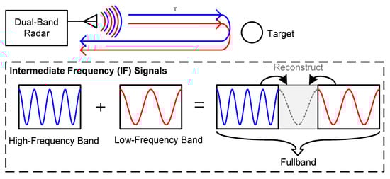
Figure 1.
Principle of the dual-band sparse synthetic bandwidth radar.
Based on the aforementioned operating principle of the dual-band sparse synthetic bandwidth radar, the architecture of the proposed terahertz dual-band radar transmitter is shown in Figure 2. The terahertz signal generated by the quad-transformer-coupled VCO is amplified through a three-stage buffer and then fed into a dual-harmonic generator to produce LB and HB signals with a frequency-doubling relationship. These signals are subsequently radiated through a dual-band antenna, thereby forming the two sub-bands required for sparse bandwidth synthesis. Furthermore, by down-converting the received echo signal using a mixer to output the IF signal, dual-band bandwidth synthesis can be implemented in the baseband.
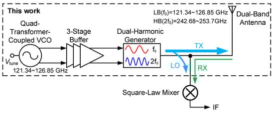
Figure 2.
Architecture of the proposed dual-band terahertz radar transmitter.
2.1. Proposed Quad-Transformer-Coupled VCO
Figure 3 illustrates the schematic of the proposed quad-transformer-coupled VCO. The core components of this oscillator comprise a quadruple-coupled transformer, a pair of cross-coupled transistors and connected via inductors, and a pair of magnetically coupled transistors and . These elements collectively form the main structure of the VCO. Inductors and share a common center tap and supply the DC power to transistors –; similarly, a DC bias voltage is provided to the gates of and through the center tap of , while frequency tuning is achieved via voltage applied to the gates of and through . This voltage alters the equivalent capacitive reactance and transconductance of the magnetically coupled transistors, thereby modulating the equivalent inductance of the resonant cavity through magnetic coupling and enabling continuous frequency control. The design ingeniously utilizes the intrinsic parasitic capacitances of the transistors to form the resonant cavity without employing any external varactors or discrete capacitors, which not only simplifies the circuit topology but also enhances stability and reliability. We adopt the simulation methodology with S-parameters as discussed in reference [13] for parasitic parameter extraction using Ansoft HFSS. The layouts of the transistors (including all metal layers, but excluding gate poly and source/drain layers), and metal interconnects between devices are imported into Ansoft HFSS for electromagnetic (EM) extraction. Corresponding S-parameter models are generated and subsequently imported into ADS for co-simulation with the schematic. During the design phase, we evaluated the impact of additional parasitic capacitance from interconnects through pre-layout simulations. The increase in this interconnect parasitic capacitance reduces the tuning range. The simulation results indicated that the parasitic capacitance has the most significant influence. With a capacitance increase of 2 fF, the of transistors and reduced the tuning range by 1.2 GHz and 0.6 GHz, respectively, whereas the and of transistors and resulted in a reduction in less than 0.2 GHz. Consequently, our layout design was optimized to minimize the additional interconnect parasitic capacitance .
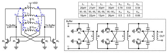
Figure 3.
Schematic of the proposed quad-transformer-coupled VCO.
In this design, frequency variation is primarily governed by two concurrent mechanisms: firstly, the variation of alters the transconductance () of the magnetically coupled transistors, thereby modifying the amplitude and phase relationships of the branch currents; secondly, directly modulates the intrinsic gate parasitic capacitances of transistors and . Figure 4 shows the simplified equivalent circuit of the proposed VCO. In this equivalent circuit, represents the parasitic capacitance in each resonant loop, while models the losses within each resonant loop. denotes the equivalent input transconductance of the magnetically coupled transistor . Based on the analysis in [14], the effective inductance seen from can be derived as
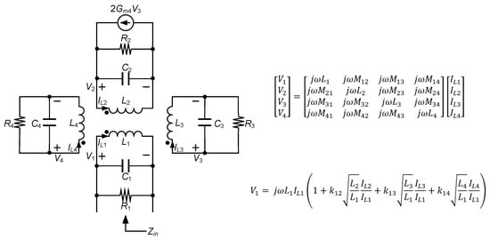
Figure 4.
Simplified equivalent circuit of the proposed VCO.
It can be observed that achieving a wide tuning range requires optimizing the coupling coefficient, inductance ratio, and current ratio to relatively high levels. However, these parameters are interdependent and constrained, and cannot be increased indefinitely.
Figure 5 illustrates the layout and cross-sectional view of the adopted octagonally symmetric quadruple-coupled transformer. Implemented using the three thick top metal layers (M9, M10, AP) provided by the technology, the transformer features inductors and constructed in a stacked and coupled configuration using M10 and M9, respectively. is formed by the parallel combination of M9 and M10, and is concentrically coupled with both and . is implemented using the aluminum cap layer (AP). The output of the VCO directly drives a common-source buffer amplifier employing neutralization capacitor technology. This buffer effectively isolates the oscillator from performance degradation due to subsequent loading stages while providing sufficient drive power for the following dual-harmonic generator.
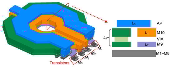
Figure 5.
Three-dimensional view of the VCO core layout.
2.2. Proposed Dual-Harmonic Generator
To simultaneously generate the fundamental and second harmonic signals, the schematic of the proposed dual-harmonic generator is shown in Figure 6a. The circuit adopts a push–push frequency doubler structure, where transistors and form a differential input common-source configuration with their drain outputs shorted together. This structure provides a broadband effect, and the conversion loss can be compensated by the active transistors. Since the input fundamental signals are differential, the fundamental signals at the two transistor drains exhibit opposite phases, while the second harmonic signals are in phase. This means the fundamental output signal generated by the dual-harmonic generator equals the difference between the fundamental output signals of the two transistors, whereas the output second harmonic equals the sum of their second harmonic output signals. Unlike conventional push–push frequency doublers that apply equal gate bias voltages to eliminate the fundamental output signal, this work applies different gate bias voltages to the two transistors to enhance the difference in fundamental signals, making them comparable to the sum of the output second harmonics, thereby enabling simultaneous output of both fundamental and second harmonic signals. This is achieved by setting independent and potentials for each transistor. Although the dual-harmonic generator unbalance causes some phase mismatch in second harmonic components, the deterioration in their sum is limiting. At the fundamental frequency of 130 GHz, when the two transistors are biased differently ( = 0.2 V, = 0.5 V), the simulated phase mismatch of the second harmonic is 19°, resulting in only a 0.12 dB loss in the second harmonic output. The dual-band matching network consists of inductor , transmission lines and , and capacitor . Inductor is used to apply the DC supply voltage while also contributing to the impedance matching. Capacitor is designed with a proper capacitance value so that it contributes to the impedance matching and provides DC blocking of . Combining inductor , transmission lines and , and capacitor , as well as the output impedance of and the input impedance of the antenna, the dual-band matching is realized. The design utilizes the frequency-dependent input impedance characteristic of transmission lines, and benefits from the stable and accurately modelable characteristic impedance of transmission lines at high frequencies, which facilitates the design and optimization of the dual-band matching.
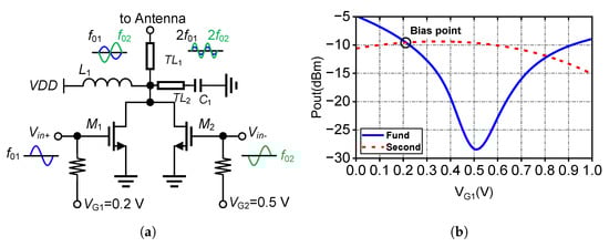
Figure 6.
(a) Schematic of the dual-harmonic generator. (b) Simulated output power of the fundamental and second harmonic versus bias voltage ( = 0.5 V, Pin = 7.5 dBm).
Figure 6b shows the simulated output power of the fundamental and second harmonic versus at 130 GHz with 7.5 dBm input power ( = 0.5 V). When = 0.2 V and = 0.8 V, the output powers of the fundamental and second harmonic are equal, with corresponding DC power consumptions of 1.73 mW and 8.42 mW, respectively. = 0.2 V is selected as the bias point to minimize DC power consumption. Finally, in co-simulation with the preceding VCO, the output power of the dual-harmonic generator versus frequency is shown in Figure 7b. It can be observed that with = 0.4∼1 V, corresponding to the VCO tuning range of 125.6∼131.1 GHz (Figure 7a), the maximum output power of the dual-harmonic generator is −9.4 dBm, with the power difference between the fundamental and second harmonic within 2.3 dB. Considering the greater path loss at the higher frequency of the second harmonic, the power of the second harmonic is appropriately set higher than that of the fundamental frequency in the simulation design. Furthermore, in real applications, the output power of the fundamental and second harmonic can be balanced by readily adjusting the tunable gate voltages and . Notably, the tuning characteristic is linear, making it suitable for FMCW radar applications.
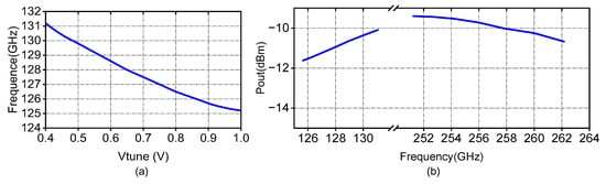
Figure 7.
(a) Simulated tuning frequency of the VCO. (b) Simulated output power of the dual-harmonic generator.
2.3. Dual-Band Antenna
To achieve monolithic integration of the transmitter system, this design employs a compact on-chip dual-band antenna, as shown in Figure 8. Its operating principle leverages the harmonic characteristics of a dipole antenna to achieve dual-band radiation. By applying image theory, the dipole antenna is simplified to a monopole antenna, enabling effective radiation in both the D-band (110∼170 GHz) and J-band (220∼325 GHz) [15], thereby covering the required fundamental and second-harmonic bands of the transmitter. A meandering structure is adopted to minimize the chip area. After co-optimization with the RF front-end circuits, the antenna achieves simulated peak gains of 2 dBi in the LB and 2.2 dBi in the HB, respectively, within a compact chip area of only 0.1 × 0.18 .
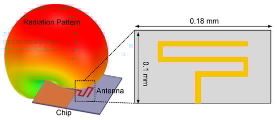
Figure 8.
Structure of the on-chip dual-band antenna and simulated radiation pattern.
3. Measurement
The proposed dual-band transmitter chip is implemented in TSMC 40 nm CMOS technology, with its chip micrograph shown in Figure 9. The chip size is 0.54 × 0.62 . For testing, the chip is mounted on a PCB using standard wire bonding. The bonding pads are placed away from the on-chip antenna to minimize radiation interference caused by the wire bonds. To enhance the antenna directivity, a detachable low-cost TPX polymethylpentene lens is placed at the front side of the chip (Figure 9c). The total DC power consumption of the chip is 136 mW. The chip measurement setup is illustrated in Figure 10. A horn antenna (with a gain of 24 dBi in the low-frequency band and 23 dBi in the high-frequency band), a R&S ZC170 and a R&S ZC330 frequency extender, and a spectrum analyzer are used to measure the radiated wave from the chip. The operating frequency ranges of the ZC170 and ZC330 extenders are 110∼170 GHz and 220∼330 GHz, respectively, covering the LB and HB of the proposed system. The frequency extenders are configured in receiver mode.
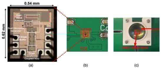
Figure 9.
The photos of (a) chip micrograph, (b) test PCB, (c) the chip package with a lens.
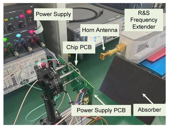
Figure 10.
Measurement setup.
Figure 11a shows the measured tuning frequency of the VCO versus the tuning voltage (). The measured fundamental frequency tunes from 121.34 GHz to 126.85 GHz as varies from 0.3 V to 1 V. The measured frequency range is lower than the simulation results due to the underestimation of circuit parasitic parameters during the design, with a deviation of less than 3.3%. This deviation is close to the 3.2% deviation reported in reference [13], which was obtained using a simulation with S-parameters. The measured EIRP across the tuning range is presented in Figure 11b. The results demonstrate the transmitter’s capability to simultaneously transmit signals in both the LB (121.34∼126.85 GHz) and HB (242.68∼253.7 GHz) bands, achieving a maximum EIRP of −7.95 dBm in the LB and −7.86 dBm in the HB. With the lens, the peak EIRP in both the LB and HB can be further increased to 10.05 dBm and 11.04 dBm, respectively. The measured radiation patterns of the dual-band are shown in Figure 12. From the test results, it can be obtained that the half-power beamwidths at 124 GHz and 248 GHz are 60° and 40°, respectively.
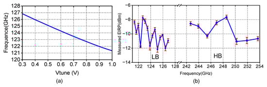
Figure 11.
(a) Measured tuning frequency range of the VCO. (b) Measured transmitter EIRP versus frequency (without lens); data are presented as mean ± SD.
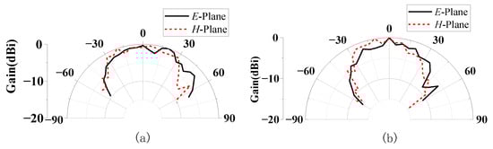
Figure 12.
Measured radiation patterns of the dual-band antenna at (a) LB: 124 GHz and (b) HB: 248 GHz.
4. Conclusions
This paper has presented and implemented a monolithic terahertz radar transmitter front-end based on a single-path-reuse dual-band architecture. The chip was fabricated in a 40 nm CMOS technology, integrating a quad-transformer-coupled VCO, a novel dual-harmonic generator with asymmetric bias, and a dual-band antenna. Table 1 summarizes its performance and comparisons with the other state-of-the-art transmitter in silicon. By simultaneously generating two frequency bands within a single compact signal path, the design theoretically enables a synthesized bandwidth of 132.36 GHz. This transmitter is suitable for low-cost, highly integrated terahertz wideband sparse synthetic bandwidth radar applications.

Table 1.
Comparison of the CMOS state-of-the-art THz transmitter.
Author Contributions
Conceptualization, A.H. and X.Y.; methodology, A.H. and X.Y.; software, A.H., L.S. and Y.W.; validation, A.H., L.S. and Y.W.; formal analysis, A.H. and X.Y.; investigation, A.H.; resources, X.Y.; data curation, A.H.; writing—original draft preparation, A.H. and L.S.; writing—review and editing, A.H. and X.Y.; visualization, A.H. and L.S.; supervision, X.Y.; project administration, X.Y.; funding acquisition, X.Y. All authors have read and agreed to the published version of the manuscript.
Funding
This work was supported in part by Guangdong Natural Science Funds, 2022B1515020039; National Natural Science Foundation of China, 62334005, 62271215, 62321002, and 62271210; the GJYC program of Guangzhou, 2024D03J0006; program under 2023ZT10X148 and 2025A04J5081.
Data Availability Statement
Data are contained within the article.
Conflicts of Interest
The authors declare no conflicts of interest.
References
- Ahmad, W.A.; Kucharski, M.; Ergintav, A.; Ng, H.J.; Kissinger, D. A Planar Differential Wide Fan-Beam Antenna Array Architecture: Modular high-gain array for 79-GHz multiple-input, multiple-output radar applications. IEEE Antennas Propag. Mag. 2021, 63, 21–32. [Google Scholar] [CrossRef]
- Chen, B.; Zong, Z. An E-Band FMCW Radar Receiver with Arbitrary-Path Spillover Cancellation. IEEE J. Solid-State Circuits 2025, 60, 1619–1631. [Google Scholar] [CrossRef]
- Welp, B.; Hansen, S.; Briese, G.; Küppers, S.; Thomas, S.; Bredendiek, C.; Pohl, N. Versatile Dual-Receiver 94-GHz FMCW Radar System with High Output Power and 26-GHz Tuning Range for High Distance Applications. IEEE Trans. Microw. Theory Tech. 2020, 68, 1195–1211. [Google Scholar] [CrossRef]
- Patole, S.M.; Torlak, M.; Wang, D.; Ali, M. Automotive radars: A review of signal processing techniques. IEEE Signal Process. Mag. 2017, 34, 22–35. [Google Scholar] [CrossRef]
- Oyamada, Y.; Koshisaka, T.; Sakamoto, T. Experimental Demonstration of Accurate Noncontact Measurement of Arterial Pulse Wave Displacements Using 79-GHz Array Radar. IEEE Sens. J. 2021, 21, 9128–9137. [Google Scholar] [CrossRef]
- Kankuppe, A.; Park, S.; Renukaswamy, P.T.; Wambacq, P.; Craninckx, J. A Wideband 62-mW 60-GHz FMCW Radar in 28-nm CMOS. IEEE Trans. Microw. Theory Tech. 2021, 69, 2921–2935. [Google Scholar] [CrossRef]
- Sanusi, J.; Oshiga, O.; Thomas, S.; Idris, S.; Adeshina, S.; Abba, A.M. A Review on 6G Wireless Communication Systems: Localization and Sensing. In Proceedings of the 2021 1st International Conference on Multidisciplinary Engineering and Applied Science (ICMEAS), Abuja, Nigeria, 15–17 November 2021; pp. 1–5. [Google Scholar]
- Al-Eryani, J.; Knapp, H.; Kammerer, J.; Aufinger, K.; Li, H.; Maurer, L. Fully Integrated Single-Chip 305–375-GHz Transceiver with On-Chip Antennas in SiGe BiCMOS. IEEE Trans. Terahertz Sci. Technol. 2018, 8, 329–339. [Google Scholar] [CrossRef]
- Vogelsang, F.; Bott, J.; Starke, D.; Hamme, M.; Sievert, B.; Rücker, H.; Pohl, N. A Fully Integrated 0.48 THz FMCW Radar Sensor in a SiGe Technology. IEEE J. Microw. 2025, 5, 572–582. [Google Scholar] [CrossRef]
- Hasan, R.; Eissa, M.H.; Ahmad, W.A.; Ng, H.J.; Kissinger, D. Wideband and Efficient 256-GHz Subharmonic-Based FMCW Radar Transceiver in 130-nm SiGe BiCMOS Technology. IEEE Trans. Microw. Theory Tech. 2023, 71, 59–70. [Google Scholar] [CrossRef]
- Hossein Naghavi, S.M.; Seyedabbaszadehesfahlani, S.; Khoeini, F.; Cathelin, A.; Afshari, E. A 250GHz Autodyne FMCW Radar in 55nm BiCMOS with Micrometer Range Resolution. In Proceedings of the 2021 IEEE International Solid-State Circuits Conference (ISSCC), San Francisco, CA, USA, 13–22 February 2021; Volume 64, pp. 320–322. [Google Scholar]
- Hong, A.; Yi, X.; Wang, Y.; Hu, J.; He, Z.; He, G.; Yang, Y.; Lai, J.; He, H.; Su, L.; et al. A Terahertz FMCW Radar with 169-GHz Synthetic Bandwidth and Reconfigurable Polarization in 40-nm CMOS. In Proceedings of the 2025 IEEE Radio Frequency Integrated Circuits Symposium (RFIC), San Diego, CA, USA, 8–10 June 2025; pp. 359–362. [Google Scholar]
- Liang, C.; Razavi, B. Systematic Transistor and Inductor Modeling for Millimeter-Wave Design. IEEE J. Solid-State Circuits 2009, 44, 450–457. [Google Scholar] [CrossRef]
- Yi, X.; Boon, C.C.; Lin, J.F.; Lim, W.M. A 100 GHz transformer-based varactor-less VCO with 11.2% tuning range in 65 nm CMOS technology. In Proceedings of the 2012 Proceedings of the ESSCIRC, Bordeaux, France, 17–21 September 2012; pp. 293–296. [Google Scholar]
- Wang, Y.; Hong, A.; Lai, J.; Su, L.; Yang, Y.; Yi, X.; Cao, Y.; Qin, P.; Zhu, H. D/J-Band On-Chip Dual-Band Antenna for Low-Cost Fully Integrated Terahertz Radar. IEEE Antennas Wirel. Propag. Lett. 2025. [Google Scholar] [CrossRef]
- Sengupta, K.; Hajimiri, A. A 0.28 THz Power-Generation and Beam-Steering Array in CMOS Based on Distributed Active Radiators. IEEE J. Solid-State Circuits 2012, 47, 3013–3031. [Google Scholar] [CrossRef]
- Kucharski, M.; Ahmad, W.A.; Ng, H.J.; Kissinger, D. Monostatic and Bistatic G-Band BiCMOS Radar Transceivers with On-Chip Antennas and Tunable TX-to-RX Leakage Cancellation. IEEE J. Solid-State Circuits 2021, 56, 899–913. [Google Scholar] [CrossRef]
- Grzyb, J.; Statnikov, K.; Sarmah, N.; Heinemann, B.; Pfeiffer, U.R. A 210–270-GHz Circularly Polarized FMCW Radar with a Single-Lens-Coupled SiGe HBT Chip. IEEE Trans. Terahertz Sci. Technol. 2016, 6, 771–783. [Google Scholar] [CrossRef]
- Mostajeran, A.; Naghavi, S.M.; Emadi, M.; Samala, S.; Ginsburg, B.P.; Aseeri, M.; Afshari, E. A High-Resolution 220-GHz Ultra-Wideband Fully Integrated ISAR Imaging System. IEEE Trans. Microw. Theory Tech. 2019, 67, 429–442. [Google Scholar] [CrossRef]
- Li, H.; Richard, K.; Bodet, D.; Ebrahimi, N. Double HOOK: A 140 GHz 15 Gb/s Reconfigurable 3-Level ASK Modulator with Constant Input Impedance for High-Speed Connectivity. IEEE Microw. Wirel. Technol. Lett. 2025, 35, 872–875. [Google Scholar] [CrossRef]
- Ng, H.J.; Kucharski, M.; Ahmad, W.; Kissinger, D. Multi-Purpose Fully Differential 61- and 122-GHz Radar Transceivers for Scalable MIMO Sensor Platforms. IEEE J. Solid-State Circuits 2017, 52, 2242–2255. [Google Scholar] [CrossRef]
Disclaimer/Publisher’s Note: The statements, opinions and data contained in all publications are solely those of the individual author(s) and contributor(s) and not of MDPI and/or the editor(s). MDPI and/or the editor(s) disclaim responsibility for any injury to people or property resulting from any ideas, methods, instructions or products referred to in the content. |
© 2025 by the authors. Licensee MDPI, Basel, Switzerland. This article is an open access article distributed under the terms and conditions of the Creative Commons Attribution (CC BY) license (https://creativecommons.org/licenses/by/4.0/).