Abstract
Nowadays, Finite Impulse Response (FIR) filters are used to change the attributes of a signal in the time or frequency domain. Among FIR filters, a reconfigurable filter has the advantage of changing the coefficient in real-time, while performing the operation. In this paper, the Anti-Symmetric Product Coding (APC) and Odd Multiple Storage (OMS) modules are utilized to implement the reconfigurable FIR filter (RFIR–APC–OMS). Herein, the APC–OMS module is used to reduce the area of the RFIR architecture. The performance of the RFIR–APC–OMS is analyzed in terms of: area, power, delay, LUT, flip flop, slices, and frequency. RFIR–APC–OMS has reduced 3.44% of area compared to the existing RFIR architecture employing the Dynamic Reconfigurable Partial Product Generator (DRPPG) module.
1. Introduction
The FIR filter is the most commonly used filter in numerous Digital Signal Processing (DSP) applications, like the removal of echo, speech signal processing, speaker standardization, versatile commotion evacuation, and communication [1,2]. Infinite Impulse Response (IIR) and Finite Impulse Response (FIR) filters are two kinds of advanced channels, which are utilized in the correspondence frameworks. In DSP systems, FIR configuration assumes a crucial job by changing the input information test with the ideal unit reaction of the FIR channel [3]. The most complex systems such as image processing and DSP applications are realized using the FIR filter as a basic tool because of its absolute stability as well as linear phase property [4]. In multimedia and mobile communication systems, the fastest and least difficult FIR filters are mostly used for various applications, such as: channel equalization, analog signal processing, filtering systems, and digital signal processing functions [5].
The traditional FIR filter design suffers from a major hindrance related to the number of evaluation processes, which is too high, so that it utilizes a higher filter order, larger area of the hardware, and consumes more energy when compared to the reconfigurable FIR filter [6,7]. In the conventional design, the FIR filter was implemented with the Distributed Arithmetic (DA) technique, in which the filter order increased with higher level [8,9,10,11]. Many of the existing architectures have been designed by using various types of FIR filter, such as: the linear-based FIR filter [12], parallel-based FIR filter [13], low-power-multiplier FIR filter [14], and DA-based FIR filter [15].
The above-mentioned conventional designs occupy high hardware resources and provide low efficiency. Meanwhile, most of the conventional designs are not concentrating on the reconfigurable design. An innovative scheme is proposed in [16,17], which helps to design a block-based RFIR structure easily. Yet, these architectures require more hardware to perform and filter operations and do not perform the reconfigurable process. As a result, the RFIR filter block-based model is only applicable for adaptive filters and 2-dimensional filters [18]. To solve this hindrance, the RFIR–APC–OMS (Anti-Symmetric Product Coding–Odd Multiple Storage) architecture is introduced in this paper.
The scientific contributions of this work are as follows:
- Due to the usage of conventional multipliers and adders, the hardware utilization of the filter has been increased to a great extent. The less combinational block adder and multiplier help to raise the filter performance effectively.
- Carry Look ahead adder (CLA) and Wallace tree multiplier (WTM) both play an important role in minimizing the energy consumption of the proposed architecture.
- The APC–OMS structure helps to redesign the Dynamic Reconfigurable Partial Product Generator (DRPPG) module, which in turn occupies less area and less delay.
- The proposed architecture was evaluated in case of Field Programmable Gate Array (FPGA) and Application Specific Integrated Circuit (ASIC) performance for different architectures. The overall performance of the RFIR–APC–OMS architecture is better than the existing architectures.
The organization of the paper is given as follows. Section 2 describes a general review of previously published papers on RFIR filter architecture. Section 3 demonstrates the WTM algorithm and CLA addition operation based on RFIR architecture. Section 4 presents a comparative analysis of the RFIR–APC–OMS filter and conventional methods based on experimental result. In Section 5, the overall conclusion of our work is given.
2. Related Works
Ramanathan et al., in Ref. [19], introduced a high-throughput and high-speed adaptive filter with DA technique. In the low-power adaptive FIR filter, the Least Mean Square (LMS) method was used to minimize the Mean Square Error (MSE) and update the weight in between the desired response and the current filter outcomes. Due to the usage of the pipeline DA table, switching activity has been increased, which consumed more power in the proposed architecture.
Krishnamoorthy et al., in Ref. [20], introduced a reconfigurable FIR filter in the Very Large-Scale Integration (VLSI) domain. In this work, interpolation and a multi-standard digital up-converter has been used to limit the area and power. The multiplication process is reduced in each input sample. In addition, a binary common sub-expression algorithm acted as an effective multiplier. The operating frequency also improved due to the usage of the binary common algorithm. However, the coefficient generation process was not explained clearly.
Mohanty et al., in Ref. [21], proposed a reconfigurable FIR filter based on VLSI architecture by using distributed arithmetic operations. In this work, FIR filter structures were analyzed in two types, that is transpose form structure and direct form structure. From the analysis of the two structures, the transpose form FIR structure required a larger number of registers when compared with a direct-form FIR structure. The DA-based FIR filter is a reconfigurable system, which is used to achieve high scalability for some specific applications, namely, larger block-size applications. The main disadvantage of the distributed arithmetic operation-based RFIR filter was that the performance of the method was very low in ASIC implementation.
Pan and Kumar [22] implemented a FIR filter based on the bit-level optimization technique. In this work, the Multiple Constant Multiplication (MCM) algorithm was utilized to execute the FIR filter operation. MCM enables the elimination of the sub-expression process, which optimizes the adder’s tree. This proposed algorithm eliminates unwanted expressions to reduce computational time and hardware complexity. This MCM algorithm required more unwanted submodules to store the intermediate register values, which caused more power consumption and higher delay.
Seik-Jae et al., in Ref. [23], illustrated the architectural approach for implementing a low-power RFIR filter structure. This new architectural approach was applicable for a fixed filter order process which can change dynamically. Mathematical analysis of the power-saving process was explained clearly. The power and area savings were equal to 41.9% and 5.3%, respectively, compared to conventional methods with less performance degradation. The bit-level optimization-based FIR filter decreased the throughput and system speed gradually, which caused high delays.
Roy and Chandra [24] proposed a triangular common subexpression elimination algorithm using the less logical blocks in the design of FIR filters. In this work, more logical operators are required to generate the bit pattern. The subexpression process has been eliminated once the bit values were performed on the average of the triangular model. The critical path of the proposed model required four adder steps for every bit of operation. The multiplier and adder blocks were required and occupied 1418 registers.
Tan et al., in Ref. [25], presented the factor-based Recursive Least Squares (RLS) algorithm for the identification of the FIR process with input noise operation. The forgetting factor of the proposed model helped to process the recursive estimation of the noise variance. The linear array design model is used to perform the bias compensation, which varied based on different FPGA devices. The proposed FPGA implemented using Zynq FPGA occupied 11500 LUT counts, which is more for the RLS algorithm.
Sakthimohan and Deny [26] illustrated a 16-tap FIR filter using Radix-4 booth multiplier with the help of the booth decoding method. The decoder and encoder modules depended on the input bits, which was given to the filter design. The proposed design required a minimum number of steps to process the multiplication operation. Partial product operation was performed with higher power consumption (1790 W) in the multiplier module.
Sumalatha et al., in Ref. [27], proposed the VLSI implementation of the FIR filter for ECG denoising applications. In this work, a Vedic multiplier was designed to perform the multiplication operation with less power consumption. The filter model was evaluated in the different FPGA and ASIC platforms to get the area, power, and delay performances. The denoising application is implemented to remove the noise, which was presented in the ECG signals. However, the Vedic multiplier process required a multiplication for every eight-clock cycle, which increased the latency of the design model.
Patali and Kassim [28] proposed an efficient design methodology using retaining and two-level pipelining techniques to improve the performance of FIR filter architecture. In this paper, a two-level pipelining technique separated the multiplication and addition operation, which used to reduce the latency of the filter. Simulation results of a 64-tap FIR filter enabled to achieve 35%, 33.97%, 38.06%, and 29.67% improvements in critical path delay, latency, power delay product, and area delay product, respectively. When the retiming technique was applied in the design model, the addition operation was broken, which caused degradation in the filter output.
Gandhi et al., in Ref. [29], presented an FIR filter implementation using a self-tunable addition and multiplication process. Two ideal instruments were proposed in this paper. The first one reset the circuit and tuned the coefficients to a certain level. Here, the self-tuning system helped to auto-tune itself at a runtime. The second one performed the reduction of nodes of addition and multiplication operations. Meanwhile, the results showed that this design gave the highest threshold limit with a satisfactory low area and delay computation. However, a single-gate-level netlist required four adders and five multipliers, which caused 384 LUTs for a simple design model.
According to the overall analysis, real-time systems frequently have a high throughput requirement. Additionally, adaptable systems can be modified in accordance with new specifications. Furthermore, the performance enhancement obtained through parallel implementation typically calls for expensive dedicated software. It is crucial to keep an observation on the configuration files to ensure that the right bits are being utilized at the right location on the FPGA. If one bit is misplaced, the configuration as a whole is invalid. Therefore, RFIR–APC–OMS is proposed, wherein the reconfigurable hardware devices allow the creation of unique, high-performance computing circuits, as well as the flexibility of software. This adaptability enables the use of FIR-filters built into FPGAs in real-time and high-throughput applications.
3. RFIR–APC–OMS Methodology
The proposed RFIR–APC–OMS filter uses WTM and CLA, which reduced the complexity of the multiplication process when compared to a conventional multiplier design. As an alternative to shifting accumulator operation, the WTM has been employed to increase system performance while avoiding undesired blocks that could result in increased area and power consumption. The system delay is decreased using the adder to perform addition operations at a fast rate of speed. The DRPPG operation has been carried out by using APC–OMS architecture with fewer slices. Therefore, as compared to the current state-of-the-art RFIR filter designs, the proposed RFIR–APC–OMS architecture occupied less space and consumed less power in the RFIR filter design.
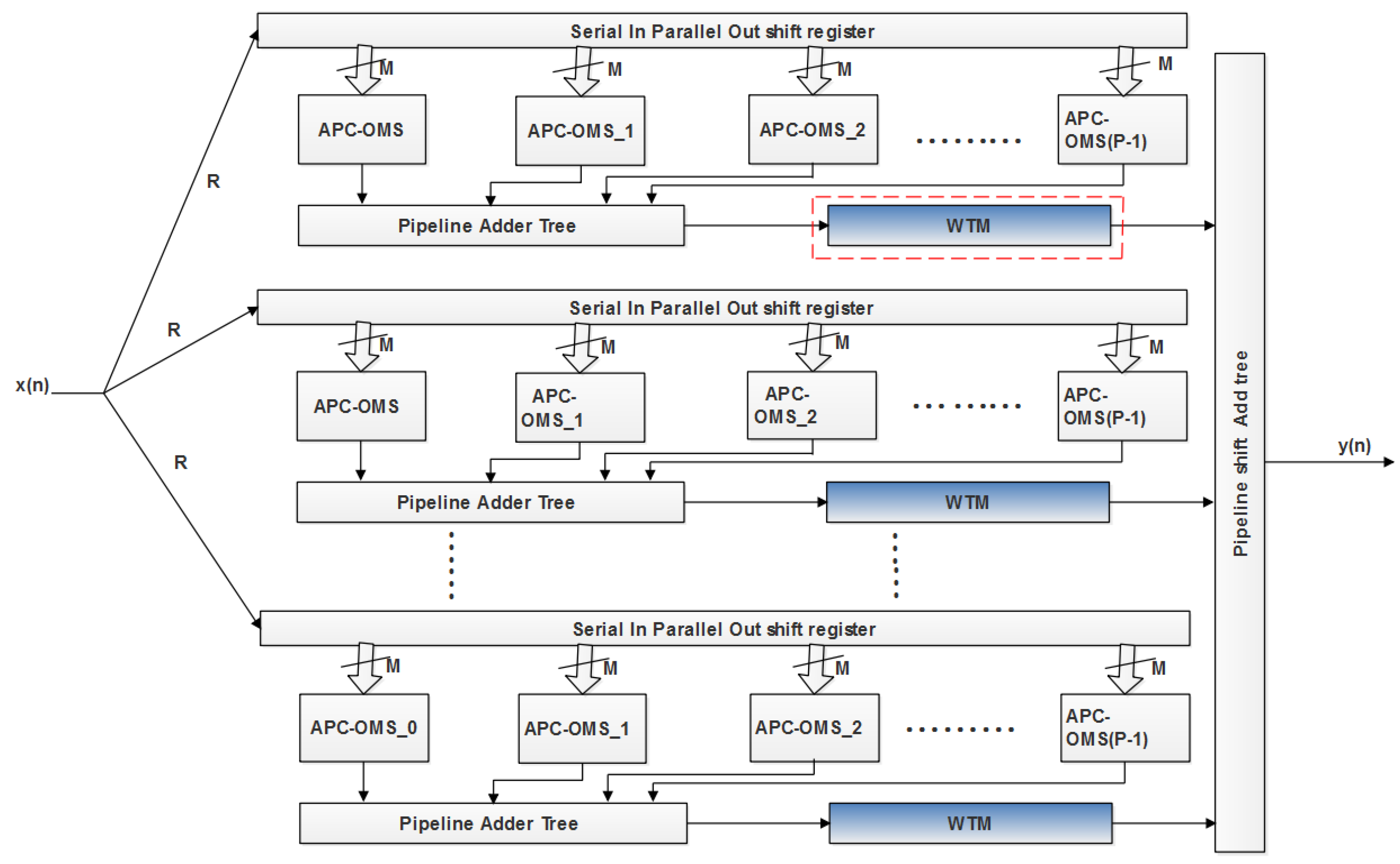
The improvement of the FPGA hardware design process is denoted as the important research area in communication systems, as it has the potential to significantly enhance the performance of a signal processing system. In the proposed method, the FPGA architecture is used to implement the RFIR filter. The block-level representation of the proposed RFIR–APC–OMS architecture is presented in Figure 1. The algorithm of the Wallace tree design based on RFIR architecture is presented in Section 3.1.
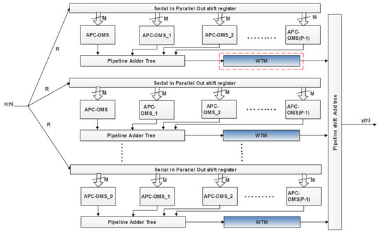
Figure 1.
Block-level illustration of the proposed RFIR–APC–OMS architecture.
3.1. RFIR Filter Model Using Wallace Tree Design
The RFIR–APC–OMS-block diagram fundamentally requires a parallel-level shifter and an accumulator for addition and multiplication operations. In the proposed method, a reusable LUT based on RAM is utilized rather than a LUT based on ROM. In the RFIR– APC–OMS strategy, an effective plan helps to minimize the count of LUT. Moreover, the CLA was used for the addition operation in the design of the FIR filter. The reconfigurable WTM-based FIR filter is utilized in the proposed method to improve the process of the RFIR filter and reduce the complexity of multiplication. Furthermore, the RFIR architecture required less hardware because it used WTM, which enhances the functionality of the entire system. In the proposed architecture, the length of the register is represented as N. However, the registers are a limited resource in FPGA devices, and LUTs in the FPGA have only two-bit registers. The distributed RAM (DRAM) is used to analyze the LUTs in the implementation of the FPGA. Moreover, denotes input bit length, and -times the clock period of the operation in the design is presented as sample duration. It is rarely suitable for applications that have more throughput.
In the implementation of LUT, the DRAM is used for less resource utilization in each bit slices. Henceforth, this work eliminates the generator of the partial inner product by Q parallel units. The Q parallel units have R-bit slices based on R-time multiplexed processes. Here, is denoted as a positive numbers or composite number, which is known as (where represents a two decimal value). In Equation (1), index value is plotted with . Here, . The value is presented in Equation (2).
The total sum of the partial product of the M samples is represented as . Here, M is represented as 222; id values are expressed as 0, 1, 2, 3, …..., and, respectively, id values are expressed as .
From Equation (3), represents the index, and denotes the index of time. The proposed architecture consists of time slots for a particular working clock period. In each single cycle period, the filter delivers a single output. The RFIR–APC–OMS architecture has units, and each unit consists of DRAM, respectively, with APC, OMS, and pipeline adder tree (PAT) modules to perform summation for the right-most portion. For processing the shift operation, the shift accumulator is used in the method based on the second summation. Generally, the RFIR processes the input by multiplying the coefficient effectively. Thus, the multiplication is performed based on the WTM. Instead of a normal digital adder, CLA is used for improving the addition performance.
3.1.1. Working Principle of APC–OMS
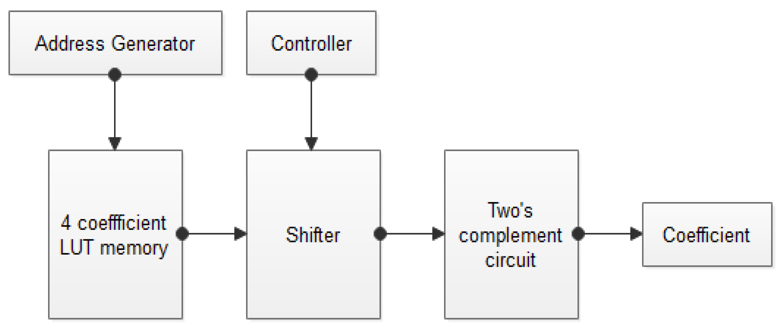
The block diagram of APC–OMS is shown in Figure 2. In this section, the process of LUT memory reduction and shift compliment coefficient are explained with the optimal designs. The design is implemented for various taps of the filter.
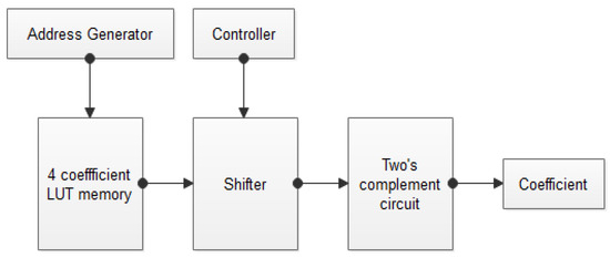
Figure 2.
Block diagram of the APC–OMS.
The 16-tap filter design generated 16 coefficients, which are stored in conventional LUT registers. The coefficient values are given in Table 1. From the conventional LUTs, the optimal LUTs are generated, which holds the four rows of coefficients, as given in Table 2. The remaining set of coefficients are generated with the help of the SC-LUT technique. The optimal SC-based LUTs are given in Table 3. The detailed explanation of the proposed work is described in the mathematical operation.

Table 1.
16 tap and 16 bit LUT table.
Table 2.
Symmetric property coefficient value.
Table 3.
Optimized LUT using the SC algorithm.
3.1.2. Mathematical Operation of the Proposed Method with an Example
- In this work, APC and OMS designs are used to implement the RFIR filter.
- In the conventional methods, 16 memory units are required to fetch the 16 values from the respective address. The main motivation for using the APC–OMS design is to reduce the memory unit count.
- With the help of the APC–OMS design, 4 memory units (0000, 0010, 0100, and 0110) are enough to fetch the 16 values from the respective address.
- Those 4 memory units have performed the left shifting and 2′s complement operation, which helps to get the 16 data values.
Example.
Let us consider that the 1st memory unit is A = 0100.
The 1st memory unit is going to perform the left-shifting operation (<<0, <<1, <<2, <<3) that produced the shifted output, which is given in Equations (4)–(7).
After performing the shifting operation, the outputs are obtained as 0100, 1000, 0001, and 0010.
Eventually, i.e., = 0100; = 0010; = 0101; = 1000.
These shifted outputs are performed as the 2′s complement, which is given in Equations (8)–(11).
- 2′s complement of is 1100;
- 2′s complement of is 1110;
- 2′s complement of is 1011;
- 2′s complement of is 1000.
As per the 2′s complement output, the 1st memory unit 0100 will fetch the data from the four addresses (1100, 1110, 1011, 1000). Similarly, the remaining memory units (0000, 0100, and 0110) are performed in the APC–OMS process. According to this operation, 4 memory units are enough to fetch the 16 values from the respective memory address.
- The optimal CLA and WTM are used in the shift accumulator module.
- Due to the usage of the optimal logical block, the hardware utilization of the RFIR filter has been reduced.
- Moreover, these optimal designs have a small delay only used to increase the speed of the RFIR filter architecture.
- The SC-based LUT design is selected from the results with a significant area reduction when compared to previous works.
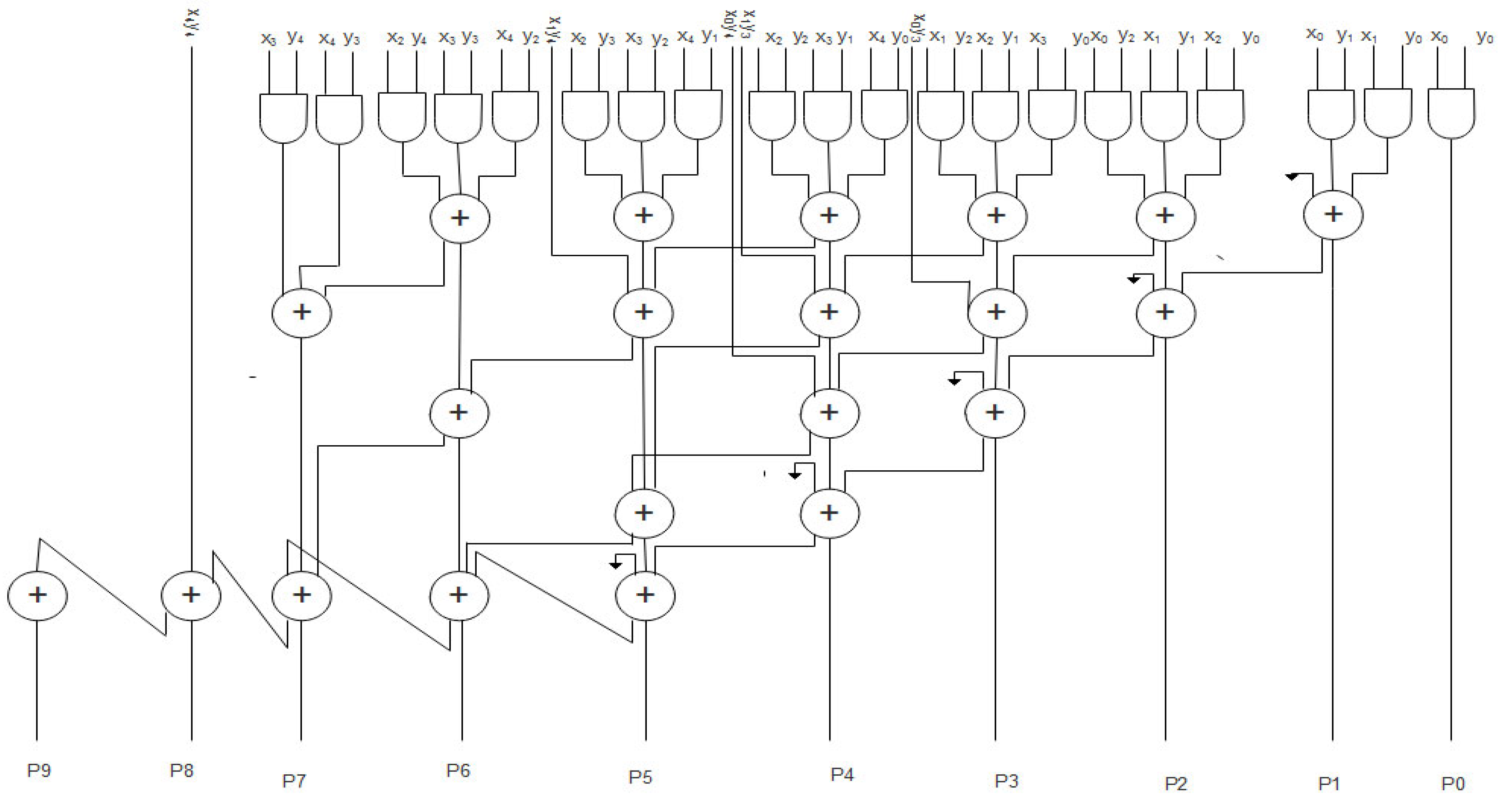
The schematic diagram of the WTM is shown in Figure 3. The output of adders is given to the input of the Wallace tree multiplier. This WTM performs the multiplication operation in an effective manner. This design avoids the unwanted blocks, which may lead to more area and power consumption.
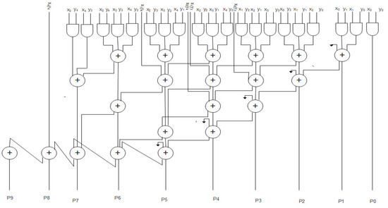
Figure 3.
Schematic of the Wallace tree multiplier.
3.1.3. Carry Look-Ahead Adder Design
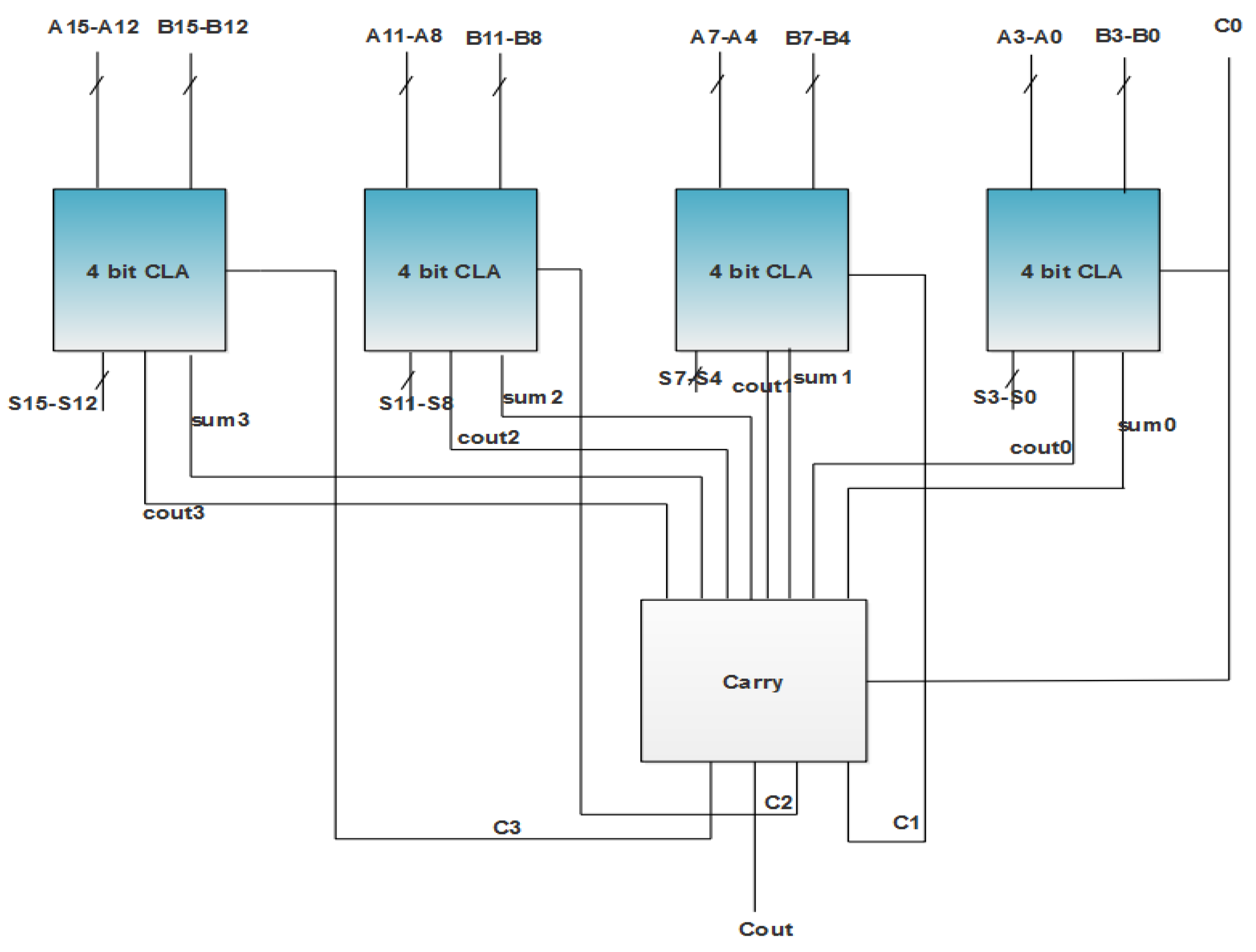
In the proposed RFIR–APC–OMS filter architecture, CLA is used for addition operations, as shown in Figure 4. The performance of the CLA is faster than the normal adders, which makes it suitable for the proposed method. Generally, four 4-bit adder blocks are required to design the 16-bit adder, as shown in Figure 4.
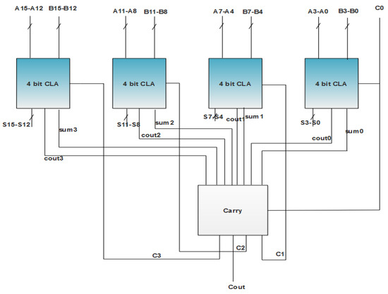
Figure 4.
CLA adder design.
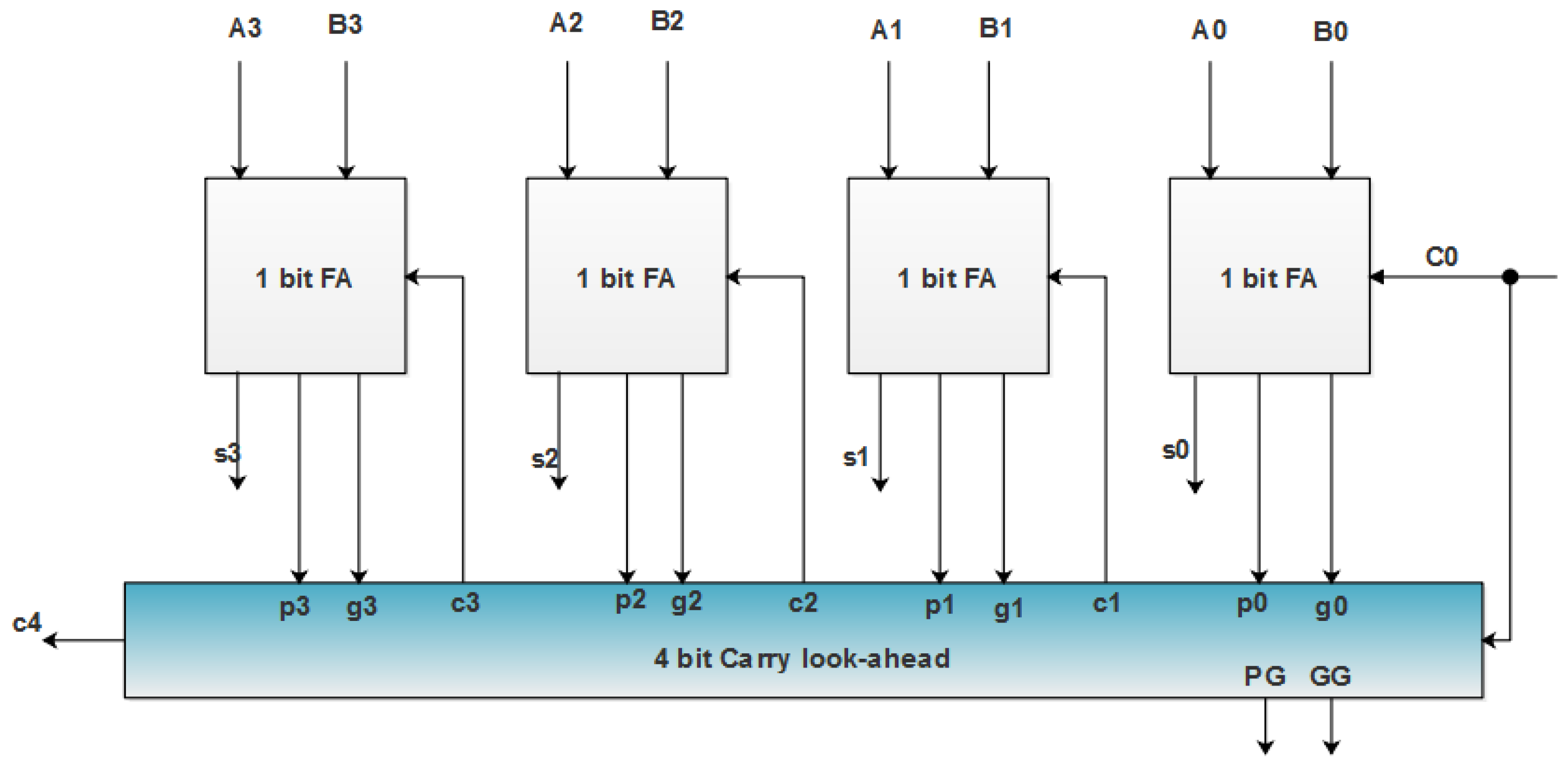
For designing 16-bit CLA adder, the 4 bit-CLA module plays a vital role. Based on the 16-bit CLA, the operations are performed and and computations are evaluated, as shown in Figure 5. The CLA adders are generally designed as 4-bit modules, which are connected together to construct large-size adders. In the RFIR–APC–OMS architecture, the 16-bit CLA is used to reduce the power, area and delay.
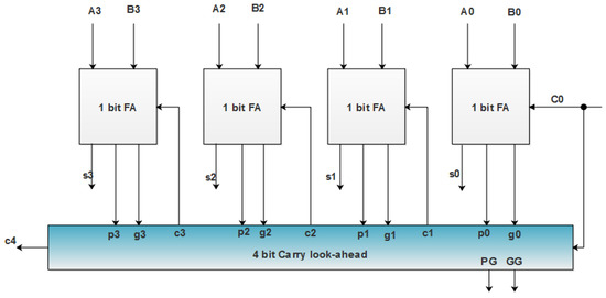
Figure 5.
Block level illustration of the 4-bit CLA design.
3.2. Coefficient Generation
The coefficient is produced from the MATLAB Filter Design and Analysis (FDA) tool, as shown in Figure 6. With the help of this tool, the coefficients are generated and used in the RFIR filter design. The filter specification is as follows:
- The direct form FIR;
- Design method—Equiripple;
- Density factor—8;
- Response type—Low pass.
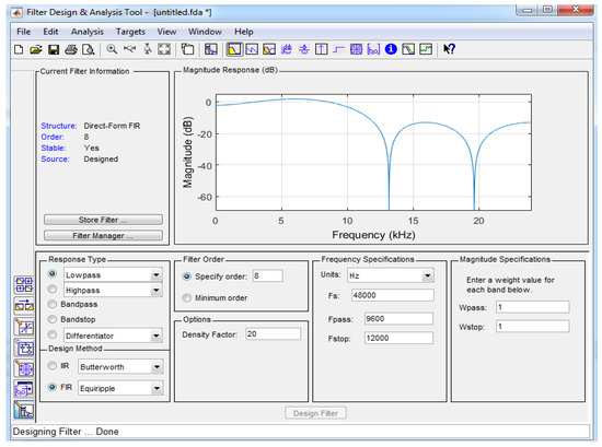
Figure 6.
FDA tool interface with selected parameters.
With the help of the filter response icon, the magnitudes are generated, which helps to optimize the overall design. From the file toolbox, the export option is utilized to generate the coefficients. These coefficients are used in the Verilog program for simulating the FIR operation.
4. Results and Discussion
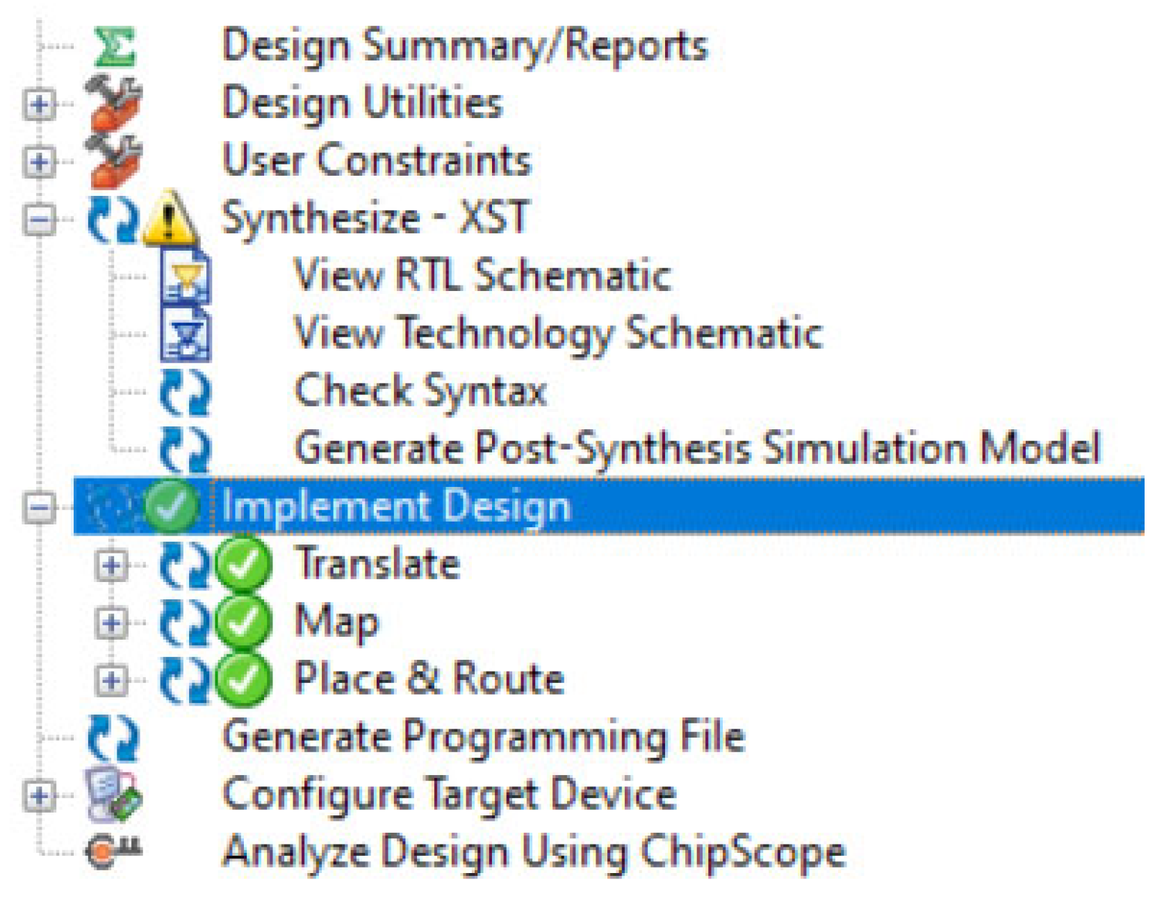
The proposed method was evaluated using a PC with 8 GB of RAM, a 1.60 GHz Intel i-5 processor, and a 1 TB hard disk. The Verilog HDL language is used to design the proposed architecture. Coefficients are generated using the MATLAB FDA tool. The Verilog HDL code is developed and simulated in the Modelsim 10.5 tool. The FPGA performance of the proposed architecture and the hardware utilization of the proposed method are calculated using the Xilinx 14.4 ISE simulator. The performance of the ASIC, such as: area, delay, and power, is calculated using a Cadence RTL compiler. The FPGA performance of the proposed architecture and the hardware utilization of the proposed method are calculated using the Xilinx 14.4 ISE simulator, which synthesizes and implements the model, as shown in Figure 7.
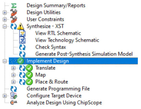
Figure 7.
Xilinx ISE synthesis and implementation design.
Xilinx 14.4 ISE is a platform used to compile combinational and sequential design models with high speed. Based on the specifications, RTL code is designed and synthesized in the Xilinx 14.4 ISE simulator. After synthetization, the frequency and the RTL schematic is observed from the synthesized report. During the implement design operation: translate, map, and place & route operations are performed for the RFIR design architecture. After implementing the design in Xilinx 14.4 ISE, the LUTs, flip fops, and slices are evaluated for the proposed RFIR design model. Xilinx 14.4 ISE was also used during experiments with the “Generate programing file” option.
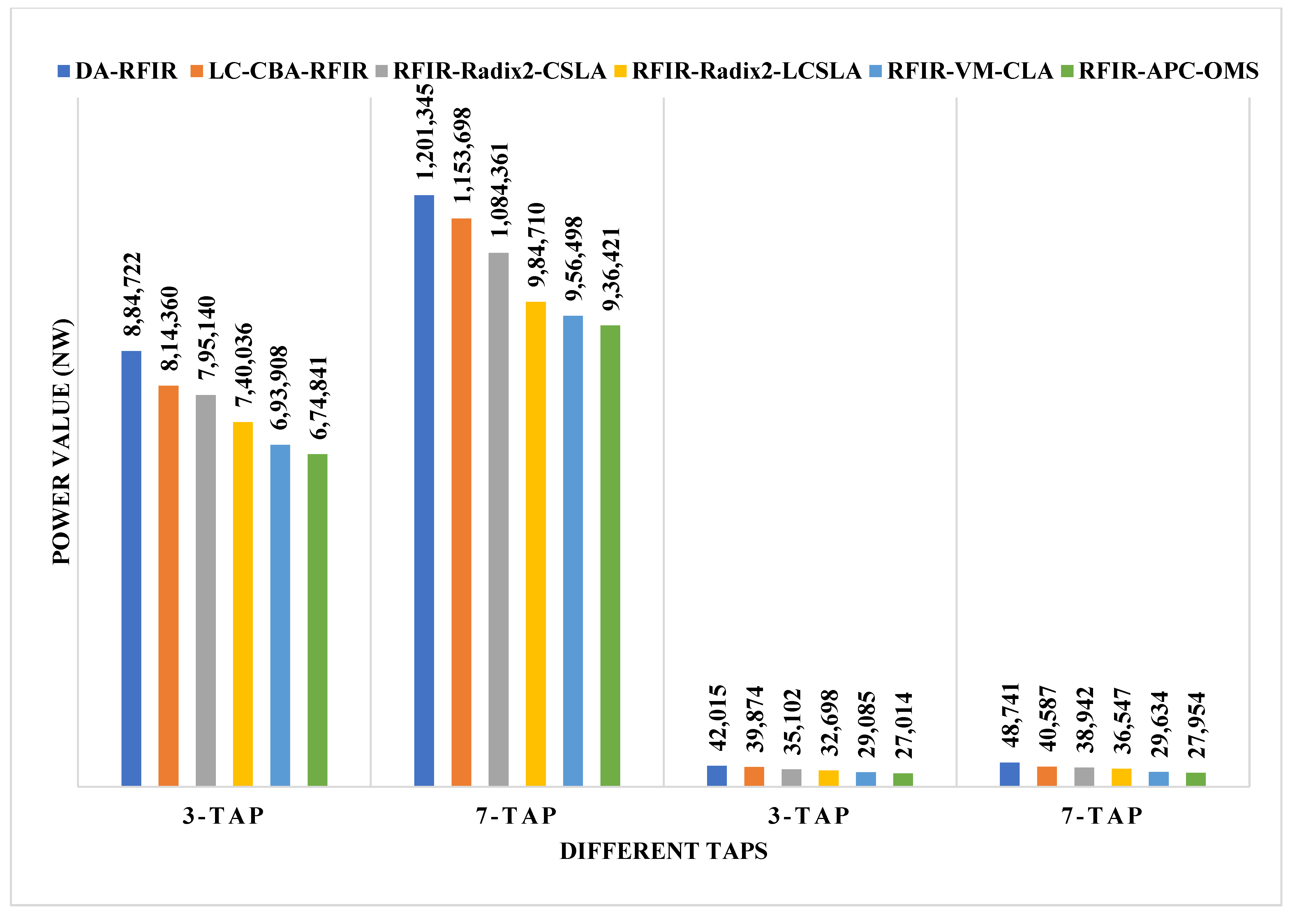
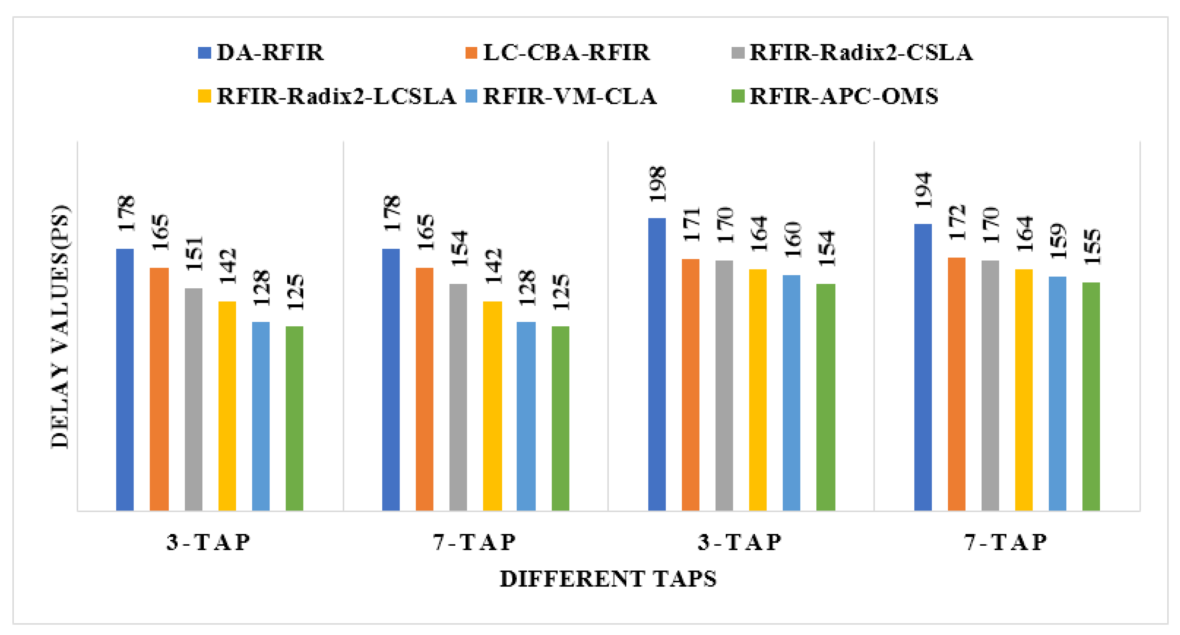
The results of the area, power, and delay performance of the 4-bit design are described in Table 4. In this comparison, DA [7], CBA [9], and R2 designs are considered as a reference and compared with the proposed filter design. RFIR–R2–CSLA, RFIR–R2–LCSLA, and RFIR–VM–CLA architectures were previously implemented by the same author, and the results are also compared with the current proposed method.
Table 4.
Area, power, and delay performance for the 4-bit design.
The comparison of area, power, and delay are shown in Figure 8, Figure 9 and Figure 10, respectively. In these graphs, the first two taps (3-tap and 7-tap) are for 180 nm technology, and the rest of the two taps (3-tap and 7-tap) are for 45 nm technology. With the help of pictorial representation, it is clear that the proposed method required less area, power, and delay when compared to the conventional designs.
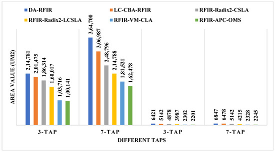
Figure 8.
Comparative analysis of area for 180 nm and 45 nm.

Figure 9.
Comparative analysis of power for 180 nm and 45 nm.
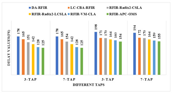
Figure 10.
Comparative analysis of delay for 180 nm and 45 nm.
The area, power, and delay performance are given in Table 5. The 8-bit RFIR is working based on the 4-bit design only. The major changes in the 8-bit RFIR filter are that the input size of the filter contains 8-bit values. With the aid of optimal designs, the ASIC performances are improved in the proposed work, compared to conventional works.
Table 5.
Area, power, and delay performance for 8-bit design.
The LUT, flip flop, slices, and frequency values are described in Table 6. Due to the usage of WTM and CLA, the RFIR design required less hardware utilization, which helps to improve the overall system performances. The different FPGA devices are used to analyze the hardware utilization of the filter design. Due to less latency, the operating speed of the proposed design also improved.
Table 6.
LUT, flop flop, slices, and frequency performances for 4-bit design.
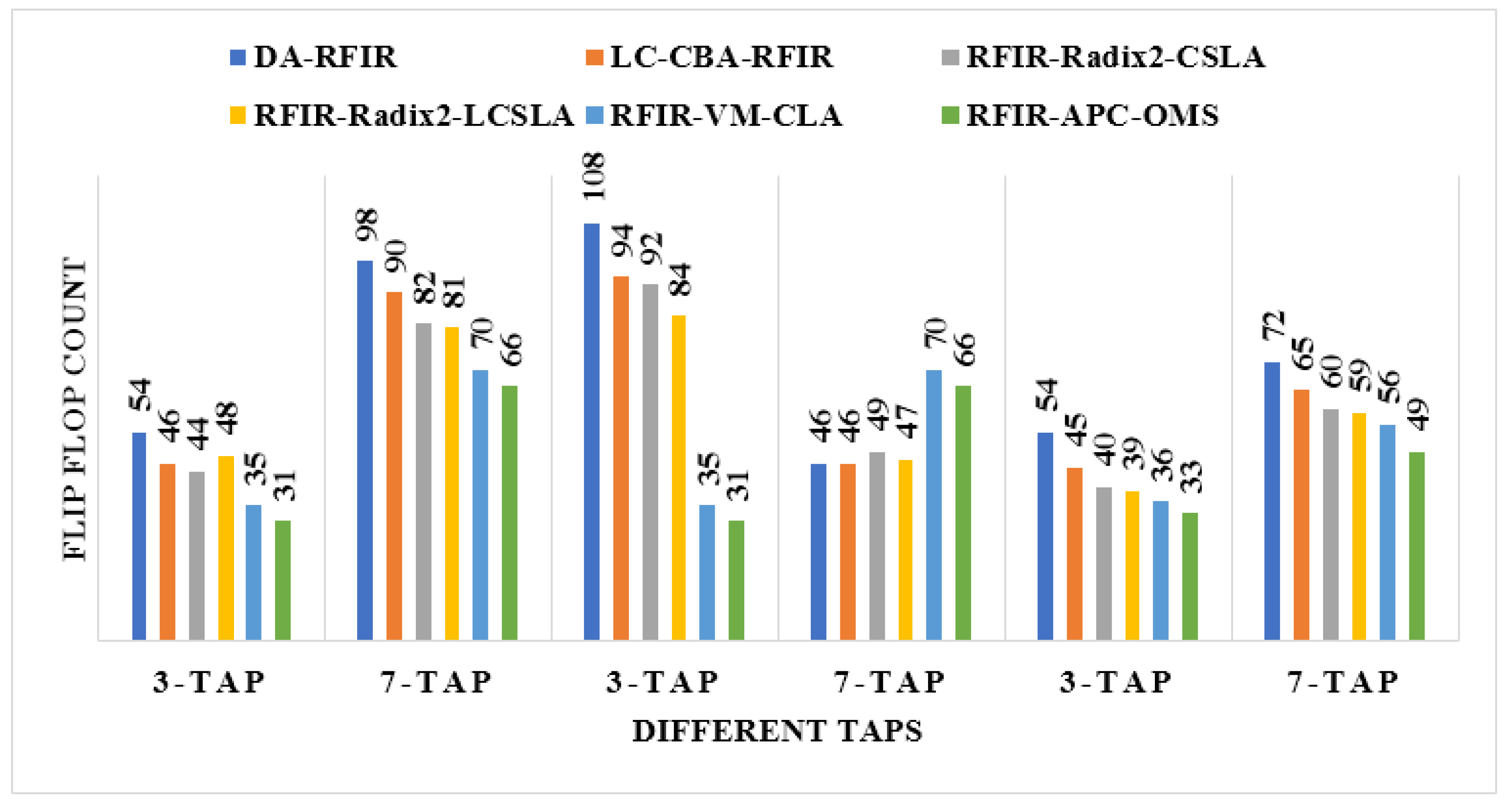
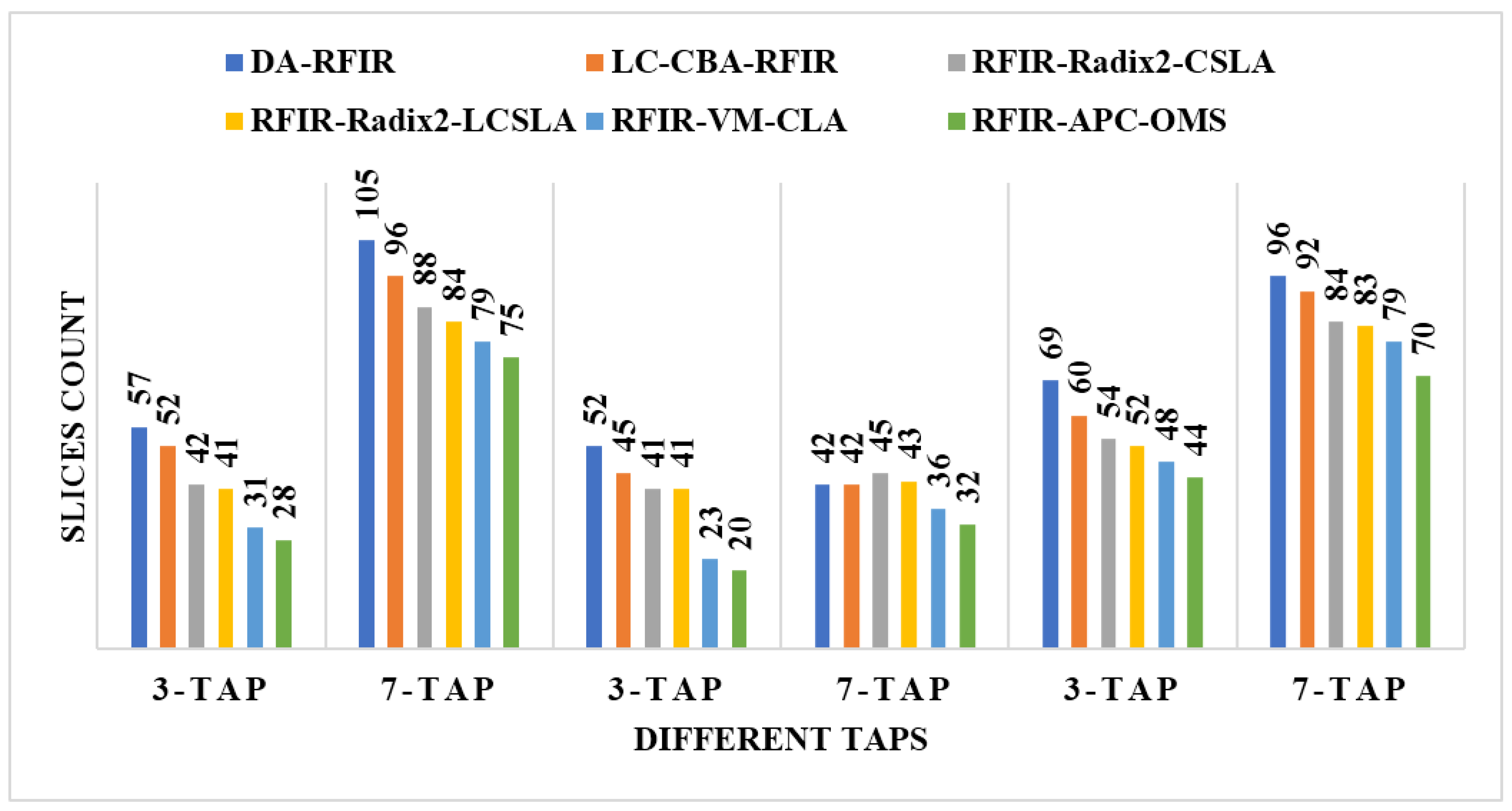
An illustration of the comparisons of the LUT, flip flop, slices, and frequency are shown in Figure 11, Figure 12, Figure 13 and Figure 14, respectively. In these graphs, the initial 3-tap and 7-tap represent Virtex 4 results. In addition, the two 3-tap and 7-tap are considered as Virtex 5, and the final 3-tap and 7-tap are considered as Virtex 6 results. As seen from these plots, the FPGA performance is improved in the RFIR–APC–OMS method compared to other existing methods.
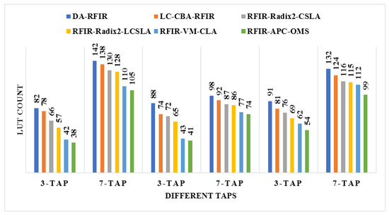
Figure 11.
Comparative analysis of LUT with various types of Virtex devices.
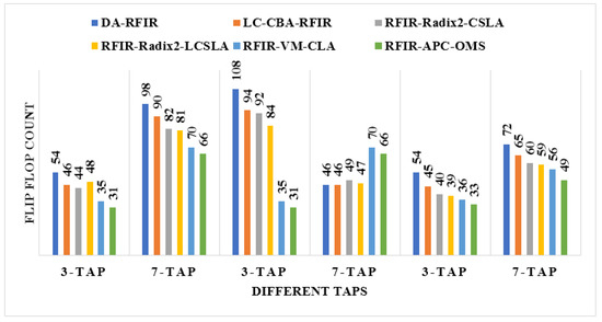
Figure 12.
Comparative analysis of flip flop with various types of Virtex devices.
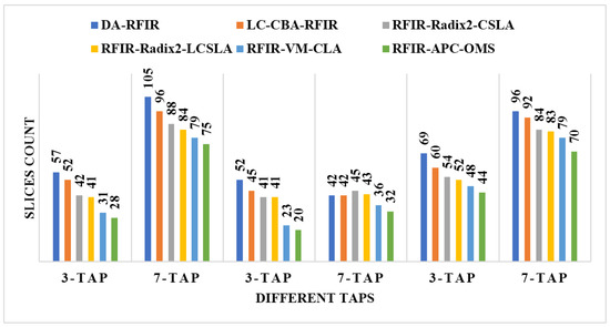
Figure 13.
Comparative analysis of slices with various types of Virtex devices.
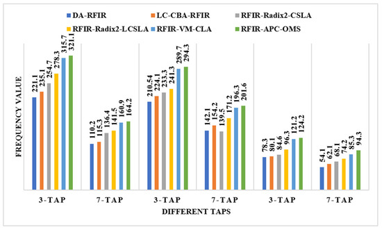
Figure 14.
Comparative analysis of the frequency with various types of Virtex devices.
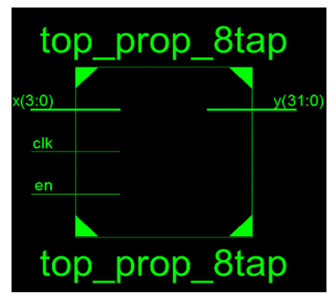
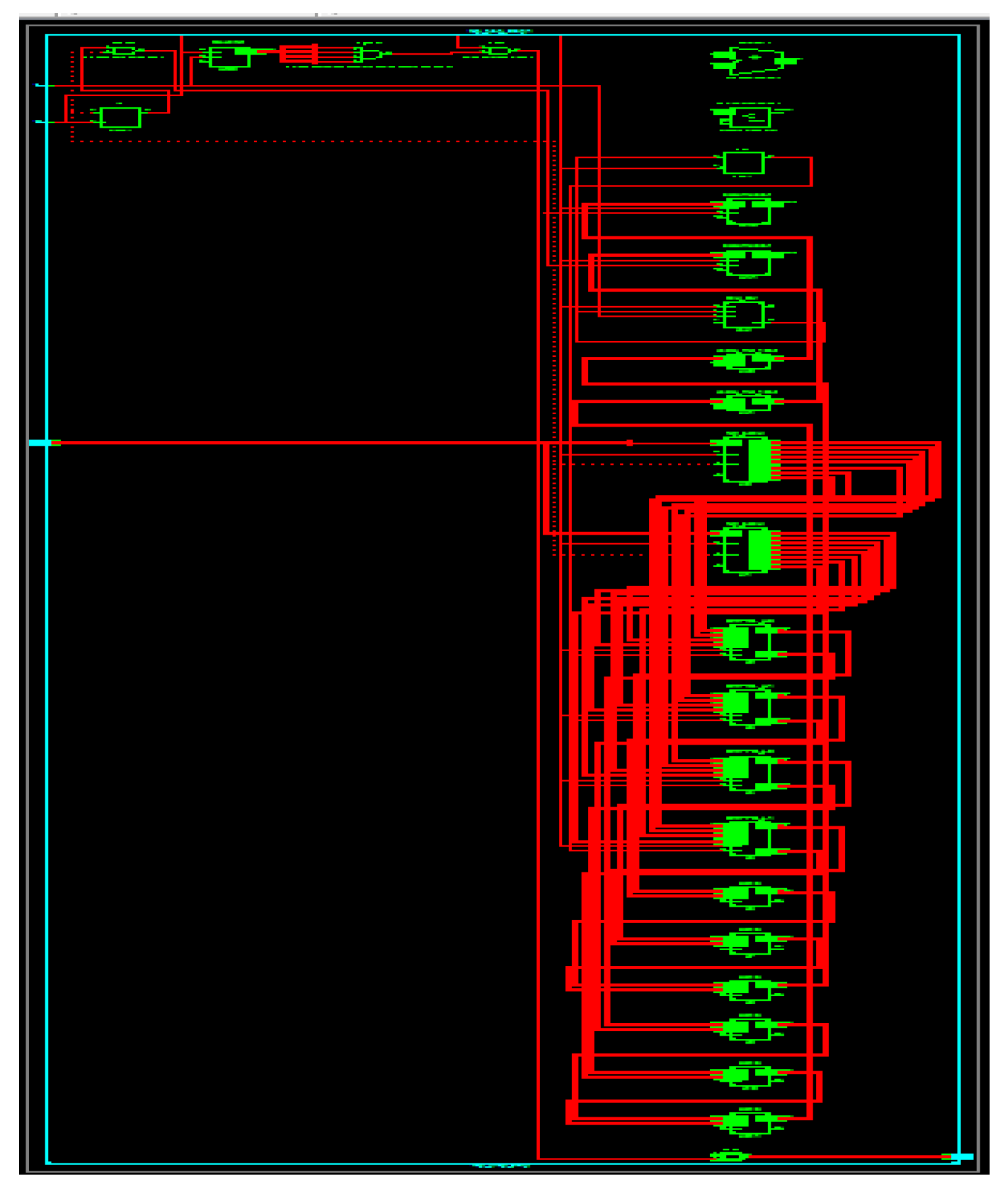
Similarly, 8-bit filter design FPGA performances are analyzed with conventional comparison. This architecture works in a similar way as the 4-bit architecture, except the design complexity is higher. The inputs given are also 8-bits in length. This 8-bit architecture also provides efficient performance results in terms of ASIC and FPGA evaluation. With the help of Xilinx RTL design, the main module and internal module RTL are handled, as shown in Figure 15 and Figure 16.
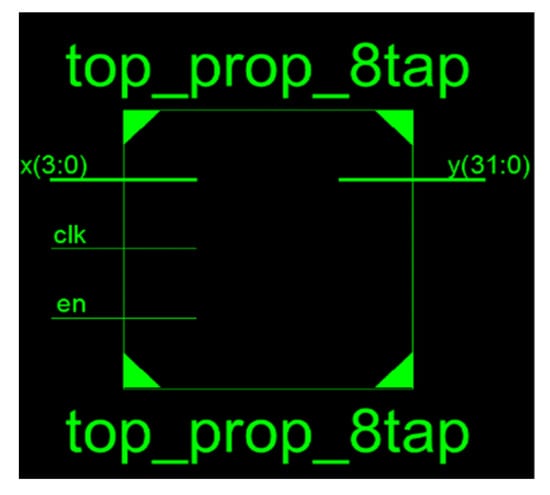
Figure 15.
Main module RTL design.
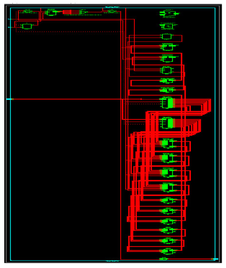
Figure 16.
RTL Schematic of the internal architecture.
The proposed filter may be used, i.e., in the medical industry, to reduce the noise present in ECG and EEG signals. The filtering operation may aid in obtaining a clear view of the medical signals, which helps to identify the condition of the patient. The proposed filter enables the solving of numerous problems in the signal processing field, depending on the signal denoising and signal enhancement with restoration. During the denoising process, the proposed filter is monitored for data loss. As we know, each signal is important to identify the health condition of the patient [27]. Additionally, RFIR filters can solve various problems occurring in the wavelet transform [30].
5. Conclusions
In this work, the FPGA and ASIC platforms are used to design the RFIR–APC–OMS architecture in the Verilog HDL language. The RFIR–APC–OMS filter has been implemented by using WTM and CLA, which decreased the complication of the multiplication process when compared to a normal multiplier design. The WTM has been used to improve the system performance as an alternative to shifting accumulator operation. The adder is used for the addition operation with high speed, which in turn reduces the system delay. APC–OMS architecture has been used to perform the equivalent DRPPG operation with fewer slices. Hence, the proposed RFIR–APC–OMS architecture required less area and less power in the RFIR filter design when compared to existing state-of-the-art RFIR filter designs. The RFIR–APC–OMS architecture enables reducing: 3.44% of the area, 2.74% of power, and 3.84% of delay (using ASIC 180 nm technology), compared to the existing Dynamic Reconfigurable Partial Product Generator (DRPPG) modules. This proposed RFIR–APC–OMS functions better for small variations in the filter order, which produces the minimal hardware usage. Additionally, the operation of filters with lower orders cannot boost the throughput of these structures. This fact will be taken into account in upcoming studies. Therefore, in the future, various types of filter architectures can be designed to further improve the performances of both FPGA and ASIC.
Author Contributions
The paper investigation, resources, data curation, writing—original draft preparation, writing—review and editing, and visualization were performed by K.S.R. The paper conceptualization and software were conducted by S.M. and A.M. The validation and formal analysis, methodology, supervision, project administration, and funding acquisition of the version to be published were conducted by P.F.-G. and P.B.D. All authors have read and agreed to the published version of the manuscript.
Funding
This research received no external funding.
Institutional Review Board Statement
Not applicable.
Informed Consent Statement
Not applicable.
Data Availability Statement
Not applicable.
Conflicts of Interest
The authors declare no conflict of interest.
References
- Naveen, N.S.; Gupta, K.A. An efficient reconfigurable FIR digital filter using modified distribute arithmetic technique. Int. J. Emerg. Technol. Adv. Eng. 2015, 5, 152–156. [Google Scholar]
- Rasekh, A.; Bakhtiar, M.S. Design of low-power low-area tunable active RC filters. IEEE Trans. Circuits Syst. II Express Briefs 2018, 65, 6–10. [Google Scholar] [CrossRef]
- Thakur, R.; Khare, K. High-speed FPGA implementation of FIR filter for DSP applications. Int. J. Model. Optim. 2013, 3, 92–94. [Google Scholar] [CrossRef]
- Bhagyalakshmi, N.; Rekha, K.R.; Nataraj, K.R. Design and Implementation of DA-based Reconfigurable FIR Digital Filter on FPGA. In Proceedings of the 2015 International Conference on Emerging Research in Electronics, Computer Science and Technology, Mandya, India, 17–19 December 2015. [Google Scholar]
- Maamoun, M.; Hassani, A.; Dahmani, S.; Ait Saadi, H.; Zerari, G.; Chabini, N.; Beguenane, R. Efficient FPGA based architecture for high-order FIR filtering using simultaneous DSP and LUT reduced utilization. IET Circuits Devices Syst. 2021, 15, 475–484. [Google Scholar] [CrossRef]
- Karthick, S.; Valarmathy, S.; Kamalanathan, C. Design and performance analysis of a reconfigurable FIR filter. Int. J. Innov. Eng. Technol. 2017, 8, 73–80. [Google Scholar]
- Meher, P.K.; Park, S.Y. High-throughput pipelined realization of adaptive FIR filter based on distributed arithmetic. In Proceedings of the 2011 IEEE/IFIP 19th International Conference on VLSI and System-on-Chip, Hong Kong, China, 3–5 October 2011. [Google Scholar]
- Bonetti, A.; Teman, A.; Flatresse, P.; Burg, A. Multipliers-driven perturbation of coefficients for low-power operation in reconfigurable FIR filters. IEEE Trans. Circuits Syst. I Regul. Pap. 2017, 64, 2388–2400. [Google Scholar] [CrossRef]
- Reddy, K.S.; Suresh, H.N. A Low Power VLSI implementation of reconfigurable FIR filter using carry bypass adder. Int. J. Intell. Eng. Syst. 2018, 11, 225–236. [Google Scholar] [CrossRef]
- Reddy, K.S.; Suresh, H.N. A low-power VLSI implementation of RFIR filter design using Radix-2 algorithm with LCSLA. IETE J. Res. 2019, 66, 741–750. [Google Scholar] [CrossRef]
- Reddy, K.S.; Suresh, H.N. FPGA implementation of reconfigurable FIR filter using Vedic design with CLA adder. Int. J. Adv. Sci. Technol. 2019, 28, 144–161. [Google Scholar]
- Tsao, Y.C.; Choi, K. Area-efficient VLSI implementation for parallel linear-phase FIR digital filters of odd length based on fast FIR algorithm. IEEE Trans. Circuits Syst. II Express Briefs 2012, 59, 371–375. [Google Scholar] [CrossRef]
- Khan, S.; Jaffery, Z.A. Low power FIR filter implementation on FPGA using parallel distributed arithmetic. In Proceedings of the 2015 Annual IEEE India Conference, New Delhi, India, 17–20 December 2015. [Google Scholar]
- Rashidi, B.; Rashidi, B.; Pourormazd, M. Design and implementation of low power digital FIR filter based on low power multipliers and adders on Xilinx FPGA. In Proceedings of the 2011 3rd International Conference on Electronics Computer Technology, Kanyakumari, India, 8–10 April 2011. [Google Scholar]
- Park, S.Y.; Meher, P.K. Efficient FPGA and ASIC realizations of DA-based reconfigurable FIR digital filter. IEEE Trans. Circuits Syst. II Express Briefs 2014, 61, 511–515. [Google Scholar] [CrossRef]
- Mohanty, B.K.; Meher, P.K. A high-performance energy-efficient architecture for FIR adaptive filter based on new distributed arithmetic formulation of block LMS algorithm. IEEE Trans. Signal. Process. 2013, 61, 921–932. [Google Scholar] [CrossRef]
- Mohanty, B.K.; Meher, P.K.; Al-Maadeed, S.; Amira, A. Memory footprint reduction for power-efficient realization of 2-D finite impulse response filters. IEEE Trans. Circuits Syst. I Regul. Pap. 2014, 61, 120–133. [Google Scholar] [CrossRef]
- Mohanty, B.K.; Meher, P.K. A high-performance FIR filter architecture for fixed and reconfigurable applications. IEEE Trans. Very Large Scale Integr. VLSI Syst. 2016, 24, 444–452. [Google Scholar] [CrossRef]
- Ramanathan, S.; Anand, G.; Reddy, P.; Sridevi, S.A. Low power adaptive FIR filter based on distributed arithmetic. Int. J. Eng. Res. Appl. 2016, 6, 47–51. [Google Scholar]
- Krishnamoorthy, R.; Kalaivaani, P.T.; Thirumurugan, P. Performance evaluation of re-configurable VLSI architecture based on finite impulse response interpolation filter. Int. J. Recent Technol. Eng. 2018, 7, 484–491. [Google Scholar]
- Mohanty, B.K.; Meher, P.K.; Singhal, S.K.; Swamy, M.N.S. A high-performance VLSI architecture for reconfigurable FIR using distributed arithmetic. Integr. VLSI J. 2016, 54, 37–46. [Google Scholar] [CrossRef]
- Pan, Y.; Meher, P.K. Bit-level optimization of adder-trees for multiple constant multiplications for efficient FIR filter implementation. IEEE Trans. Circuits Syst. I Regul. Pap. 2013, 61, 455–462. [Google Scholar] [CrossRef]
- Lee, S.J.; Choi, J.W.; Kim, S.W.; Park, J. A reconfigurable FIR filter architecture to trade off filter performance for dynamic power consumption. IEEE Trans. Very Large Scale Integr. VLSI Syst. 2010, 19, 2221–2228. [Google Scholar] [CrossRef]
- Roy, S.; Chandra, A. A triangular common subexpression elimination algorithm with reduced logic operators in FIR Filter. IEEE Trans. Circuits Syst. II Express Briefs 2020, 67, 3527–3531. [Google Scholar] [CrossRef]
- Tan, H.J.; Chan, S.C.; Lin, J.Q.; Sun, X. A new variable forgetting factor-based bias-compensated RLS algorithm for identification of FIR systems with input noise and its hardware implementation. IEEE Trans. Circuits Syst. I Regul. Pap. 2019, 67, 198–211. [Google Scholar] [CrossRef]
- Sakthimohan, M.; Deny, J. An optimistic design of 16-tap FIR filter with Radix-4 booth multiplier using improved booth recoding algorithm. Microprocess. Microsyst. 2020, 103453. [Google Scholar] [CrossRef]
- Sumalatha, M.; Naganjaneyulu, P.V.; Prasad, K.S. Low power and low area VLSI implementation of Vedic design FIR filter for ECG signal de-noising. Microprocess. Microsyst. 2019, 71, 102883. [Google Scholar] [CrossRef]
- Patali, P.; Kassim, S.T. High throughput and energy efficient FIR filter architectures using retiming and two level pipelining. Procedia Comput. Sci. 2020, 171, 617–626. [Google Scholar] [CrossRef]
- Gandhi, M.; Periyasamy, M.; Murugeswari, S.; Washburn, S.P.S. A VLSI implementation of FIR filter using self tunable addition and multiplication. Mater. Today Proc. 2020, 33, 4318–4322. [Google Scholar] [CrossRef]
- Radhakrishnan, P.; Themozhi, G. FPGA implementation of XOR-MUX full adder based DWT for signal processing applications. Microprocess. Microsyst. 2020, 73, 102961. [Google Scholar] [CrossRef]


Publisher’s Note: MDPI stays neutral with regard to jurisdictional claims in published maps and institutional affiliations. |
© 2022 by the authors. Licensee MDPI, Basel, Switzerland. This article is an open access article distributed under the terms and conditions of the Creative Commons Attribution (CC BY) license (https://creativecommons.org/licenses/by/4.0/).