Article

A Novel Fundamental Frequency Switching Operation for Conventional VSI to Enable Single-Stage High-Gain Boost Inversion with ANN Tuned QWS Controller

1
Department of Electrical and Electronics Engineering, Birla Institute of Technology, Mesra 85215, India
2
Department of Electrical Engineering, Visvesvaraya National Institute of Technology, Nagpur 440010, India
3
School of Electronics Engineering, Kalinga Institute of Industrial Technology, Bhubaneshwar 751024, India
4
Fukushima Renewable Energy Institute, AIST (FREA), Koriyama 963-0298, Japan
*
Author to whom correspondence should be addressed.
Electronics 2021, 10(20), 2499; https://doi.org/10.3390/electronics10202499
Submission received: 2 September 2021 / Revised: 7 October 2021 / Accepted: 8 October 2021 / Published: 14 October 2021
(This article belongs to the Special Issue Advances in Low Power and High Power Electronics)

Abstract

:
Single-stage high-gain inverters have recently gained much research focus as interfaces for inherent low voltage DC sources such as fuel cells, storage batteries, and solar panels. Many impedance-assisted inverters with different input stage configurations have been presented. To decrease passive component sizes, these inverters operate at high-frequency switching. The high-frequency switching optimizes the passive component sizes but introduces many challenges in the form of high-frequency inductor design, control complexity, high-frequency gate driver requirements, high semiconductor losses, and electromagnetic interferences. This article proposes a novel fundamental frequency switching operation for the conventional voltage source inverters (VSI) to operate as a single-stage high-gain inverter. As the novel operational strategy changes the behavior of conventional VSI from buck inverter to a boost inverter, it is hereafter termed as a novel inverter. By virtue of the operation strategy, switches withstand peak inverse voltage (PIV) equal to DC link voltage, unlike other impedance assisted boost inverters where PIV across switches is the amplified DC voltage. The proposed inverter can invert low-level DC voltage to high voltage AC with low total harmonic distortion (THD) in a single stage without the help of any external filter. A novel quarter-wave symmetric phase-shift controller is proposed for variable voltage and frequency control of proposed inverters tuned by a back-propagation thin-plate-spline neural network (BPTPSNN). Mathematical analysis with experimental validation is presented. Experimentation is carried out on a prototype of 2 kW for single-phase resistive load, induction motor, and non-linear loads.

1. Introduction

The limited availability of fossil fuels and increasing pollution can never fulfill the ever-increasing energy demand. It increased the thrust for renewable energy sources and allied technology to the forefront of the research arena [1]. Solar energy enjoys the prime focus among the available renewable energy sources because of its abundance and immense installation potential. The solar energy harvested by the photovoltaic (PV) panels inherently produce low voltage DC [2]. However, most electrical appliances demand AC at higher voltage levels. For this reason, inverters that convert DC to AC are essential for interfacing such renewable energy-based generators to the grid [3]. The conventional voltage source inverters (VSI) are of buck type, i.e., they produce an AC voltage level less than or equal to the available input DC link voltage. These VSIs usually employ either a step-up transformer or a back-ended boost converter to increase the voltage levels. However, these methods increase the system’s cost and complexity and compromise efficiency [4,5,6].
Further, current source inverters (CSIs) that are boost-type inverters have been employed with PV panels [7,8]. However, CSIs employ a high-value inductor at the DC link side, increasing overall system cost and weight. Moreover, control of such systems tends to be complicated as constant output voltage must be maintained.
An inverter mitigating the above issues with buck-boost capabilities termed impedance source inverters (ZSIs) has been proposed in [9], possessing the advantages of both VSI and CSI. Many improvised, enhanced, and modified topologies of ZSIs are presented in state-of-the-art [10,11,12,13,14,15,16]. However, the basic ZSI and the modified and enhanced structures provide boosted DC voltage at the interim inverting stage at the cost of passive components. This increases the component count, size, weight, and above all, the control complexity.
The passive components have been reduced by replacing the ZSI with multi-level inverters (MLIs) [17,18,19,20,21,22]. Further, a few state-of-the-art structures employ switched-capacitor inverters to boost low-level DC to high voltage AC in a single stage [22,23,24,25]. However, these inverters provide boosting, proportional to the number of semiconductors employed, i.e., more switches are employed to generate a higher level of AC voltage. This increases the semiconductor losses, thereby decreasing the efficiency, and the more the number of semiconductor switches employed, the system’s reliability decreases inversely. Moreover, the control of too many switches increases the control complexity.
Several single-stage boost inverters have been proposed [23,24,25,26]. The boost Inverter proposed in [18] and further detailed in [19] delivers low total harmonic distortion (THD) double boosted output voltage. However, the two synchronously operating boost converters should operate with a phase shift of 180° to provide doubly boosted sinusoidal output to the differentially connected load. The boost inverter discussed in [25] uses coupled inductors for boosting the voltage levels. However, this employs many inductors, which increases the size and cost of the converter. Another boost inverter with common ground for PV applications has been detailed in [26], which employs an extra capacitor for boosting purposes. This reduces the reliability and efficiency of the system. As evident from literature, many inverter topologies have been investigated for a practical high-gain DC-AC conversion with allied pros and cons.
However, the real-time application of solar panels can involve single-stage or two-stage power conversion system. The PV power conversion system’s task is twofold, i.e., the first is to extract maximum power from PV, and the second is to deliver to the application side with required power quality. Two-stage systems have these two controls decoupled i.e., maximum power tracking and AC side requirements, therefore, they are simple to implement but are bulky and costly. In contrast, single-stage conversion systems have complex control to address PV and AC side demands [27,28]. The focus of the article is a single-stage inversion system with high gain and simple control.
Class-D amplifiers with double pole filters (shown in Figure 1) have ruled the arena of high-efficiency audio and power amplifiers with a simple design, effortless control, high power, and reliable operation [29,30]. Its theoretical efficiency of 100% is often transformed into practical efficiencies of 95% and above in applications. Many controllers have been designed and developed for Class-D amplifiers to enhance intrinsic low THD and noise at output levels [31,32].
Its working has been based on sinusoidal pulse width modulation (SPWM) inverters. Many series and parallel resonant power converters have been investigated for heating purposes [33]. Nevertheless, high-frequency switching is used in all applications, raising electromagnetic interference (EMI) and electromagnetic compliance (EMC) issues. In the present work, the authors propose a new fundamental frequency switched single-stage high-gain quasi-resonant inverter. The topology of the proposed inverter mimics the Class-D amplifiers for single-phase applications.
Although the conventional H-Bridge VSI and proposed inverter structure are the same, operation-wise, it is different [34]. Conventional VSI is a buck type of inverter. However, the proposed inverter is a high-gain boost inverter. Moreover, the L and C in the conventional VSI act as a filter, but they act as voltage boosters in the proposed inverter. The proposed inverter is switched at the fundamental frequency and employs coupled resonant LC-pair to boost DC input to AC voltage with theoretically pure sinusoidal waveforms at the output. Fundamental frequency switching and lack of interim DC-link give the proposed inverter the following unique characteristics:
  • Low PIV across switches;
  • Low total blocking voltage (TBV) of converter, signifying minimal semiconductor loss;
  • Filter-free low THD output waveform;
  • Fundamental-frequency switching eliminates switching losses;
  • Supports resistive, inductive as well as non-linear loads;
  • Low passive component requirement.

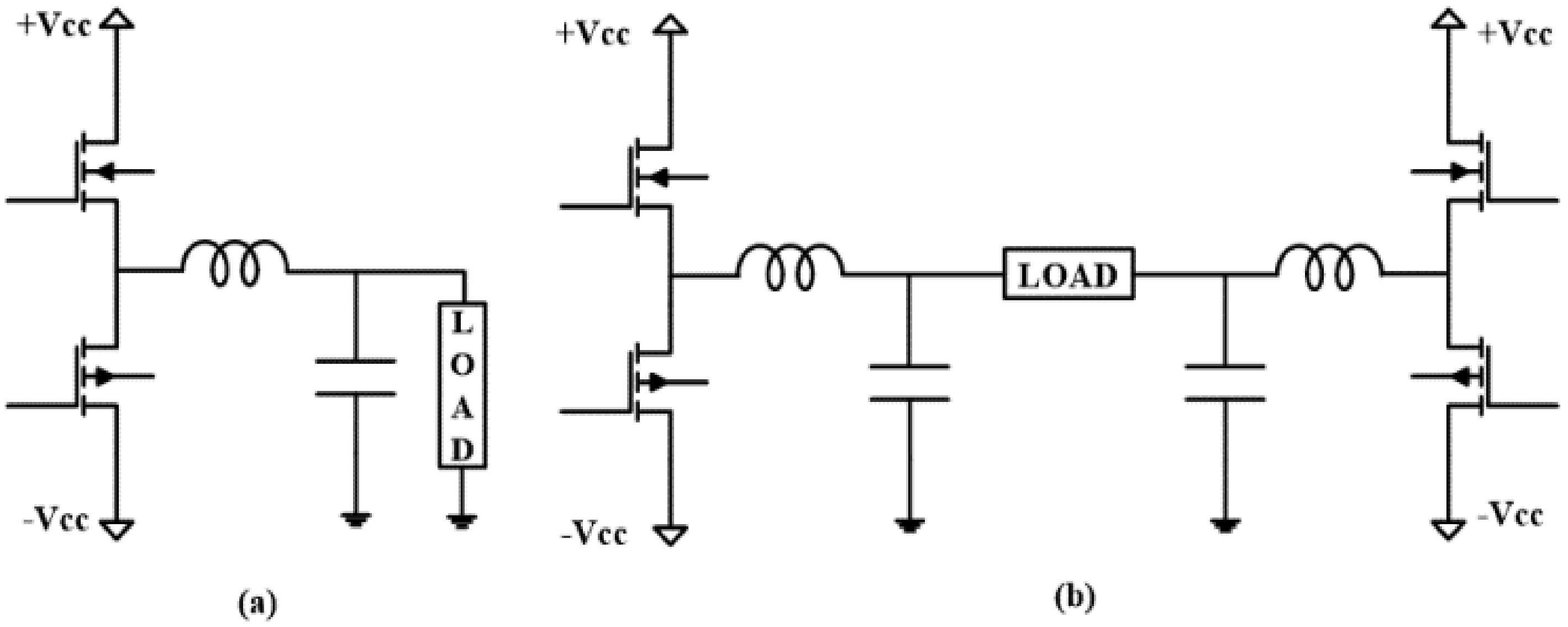
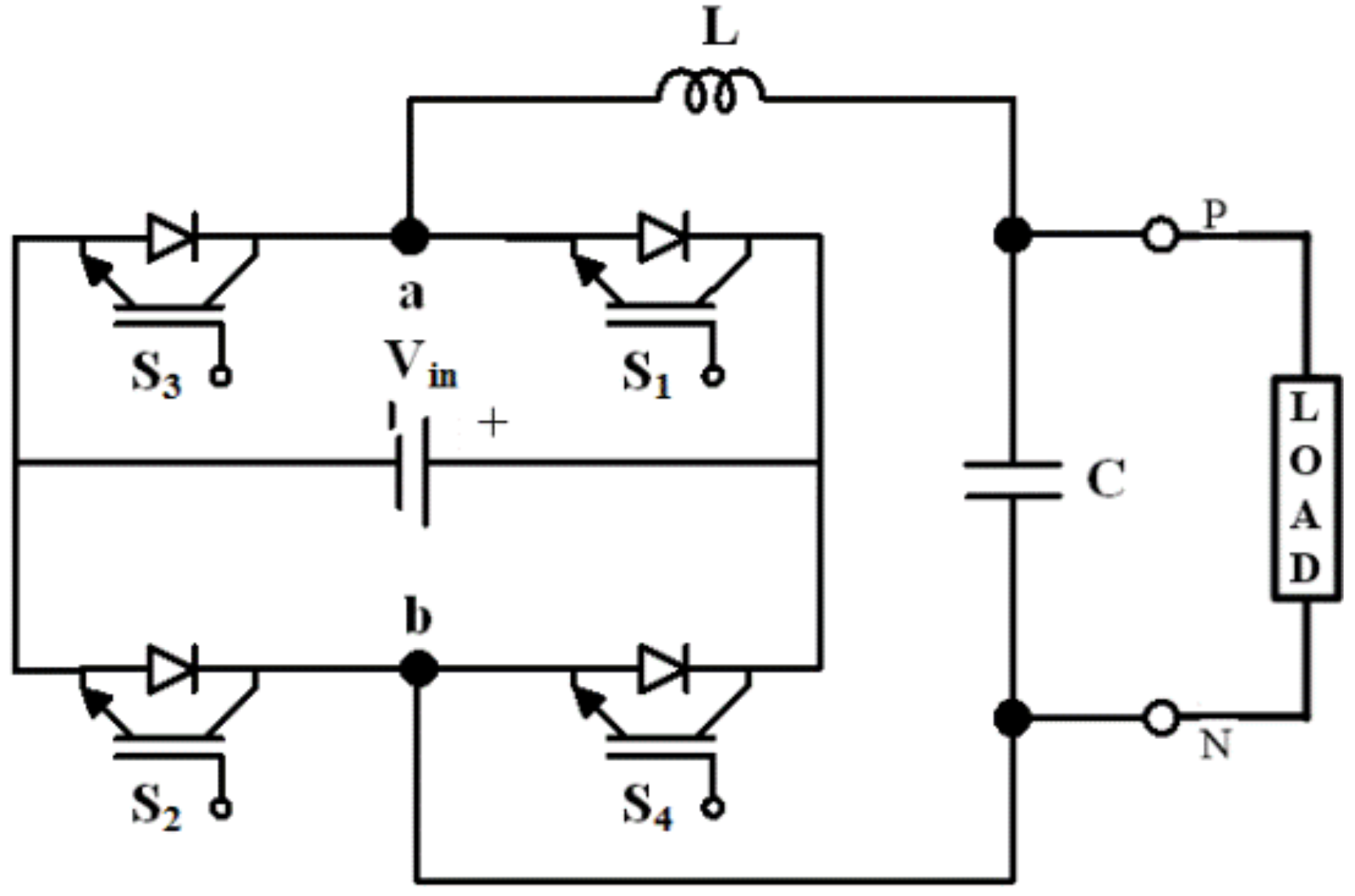
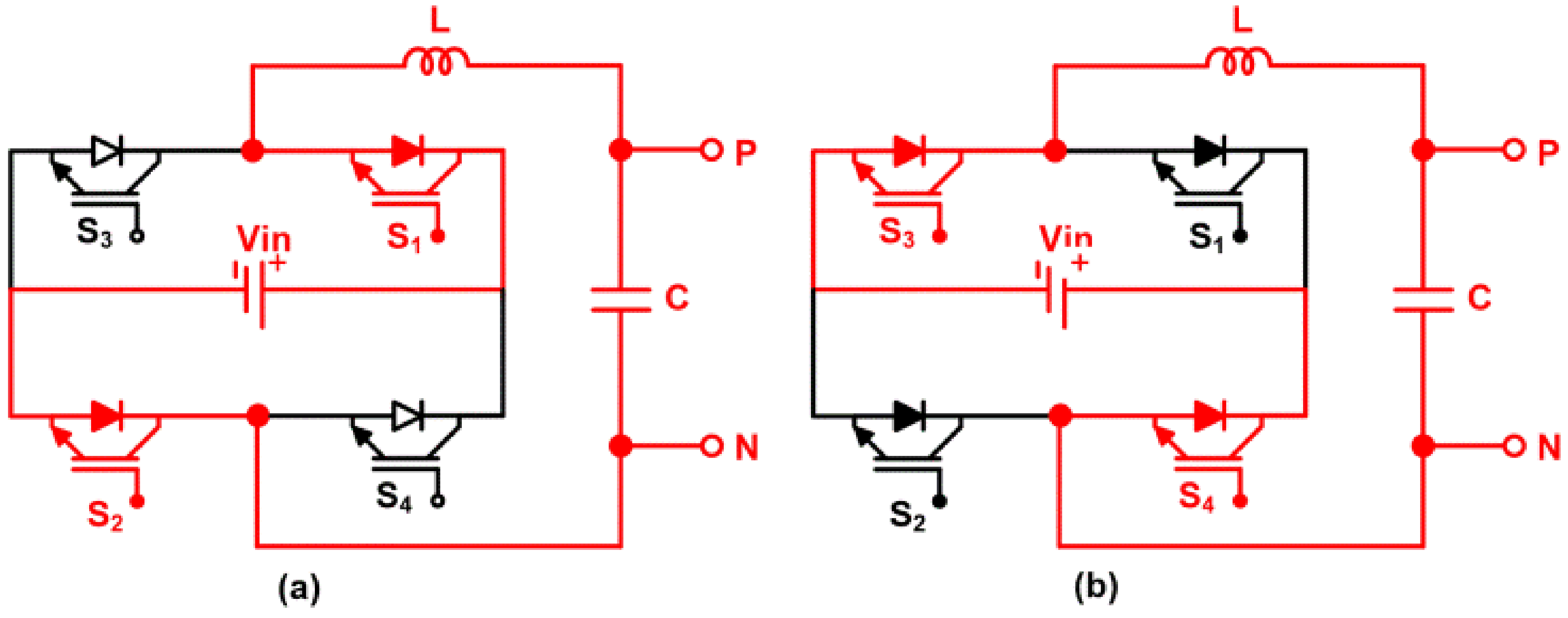
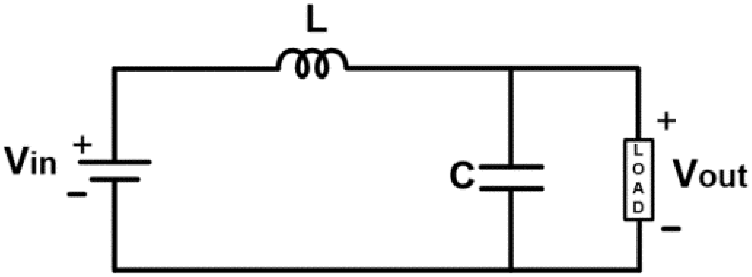
2. Circuit Operation

The proposed circuit consists of four switches and an LC pair, tuned around the fundamental frequency of operation, and the load is connected across the capacitor, as shown in Figure 2.
Switches are operated at the fundamental frequency in a complementary fashion, i.e., while S1 and S2 are ON, S3 and S4 remain OFF and vice-versa. As the input DC source is parallel to the legs, the operation is symmetrical. Operation modes are shown in Figure 3.

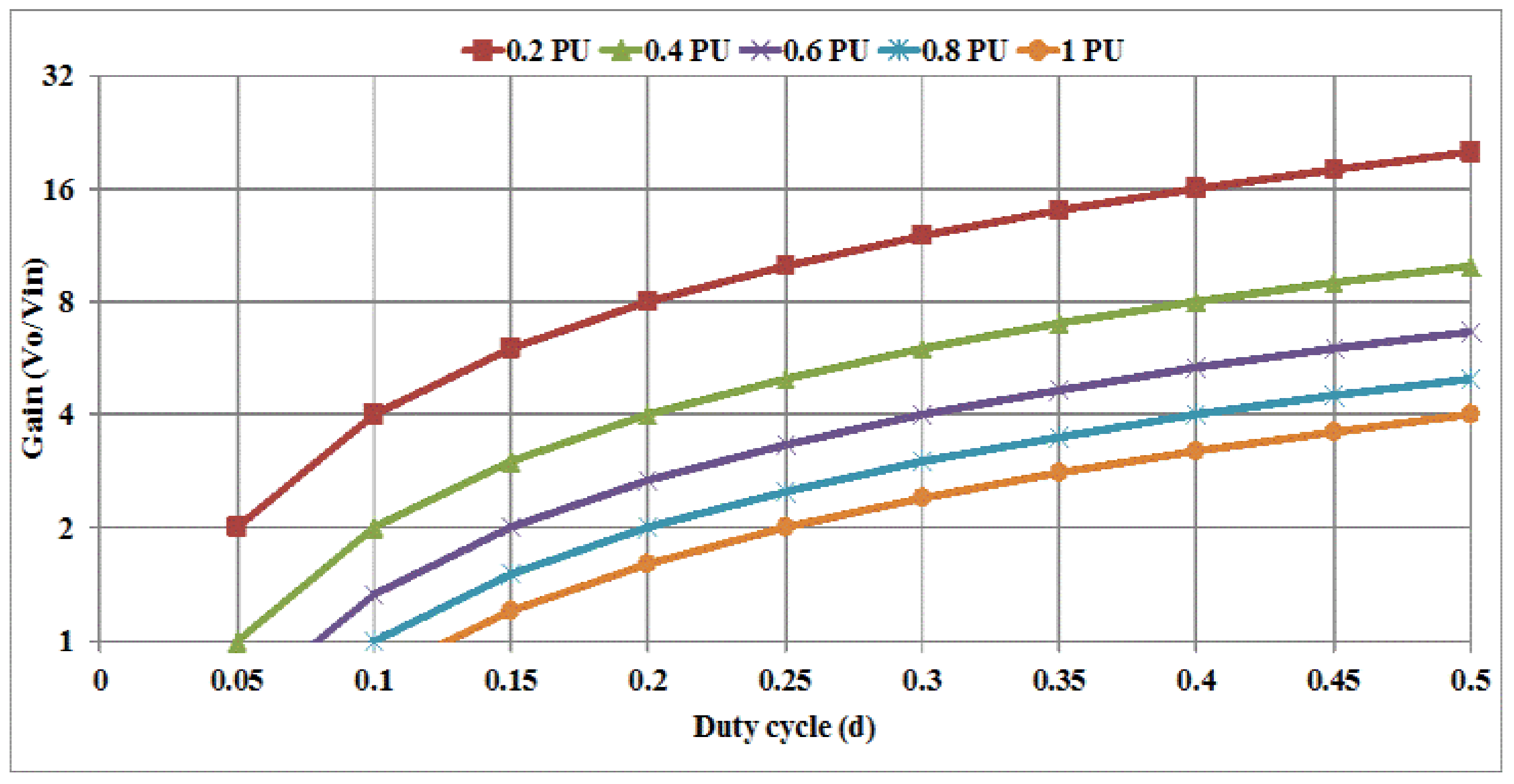
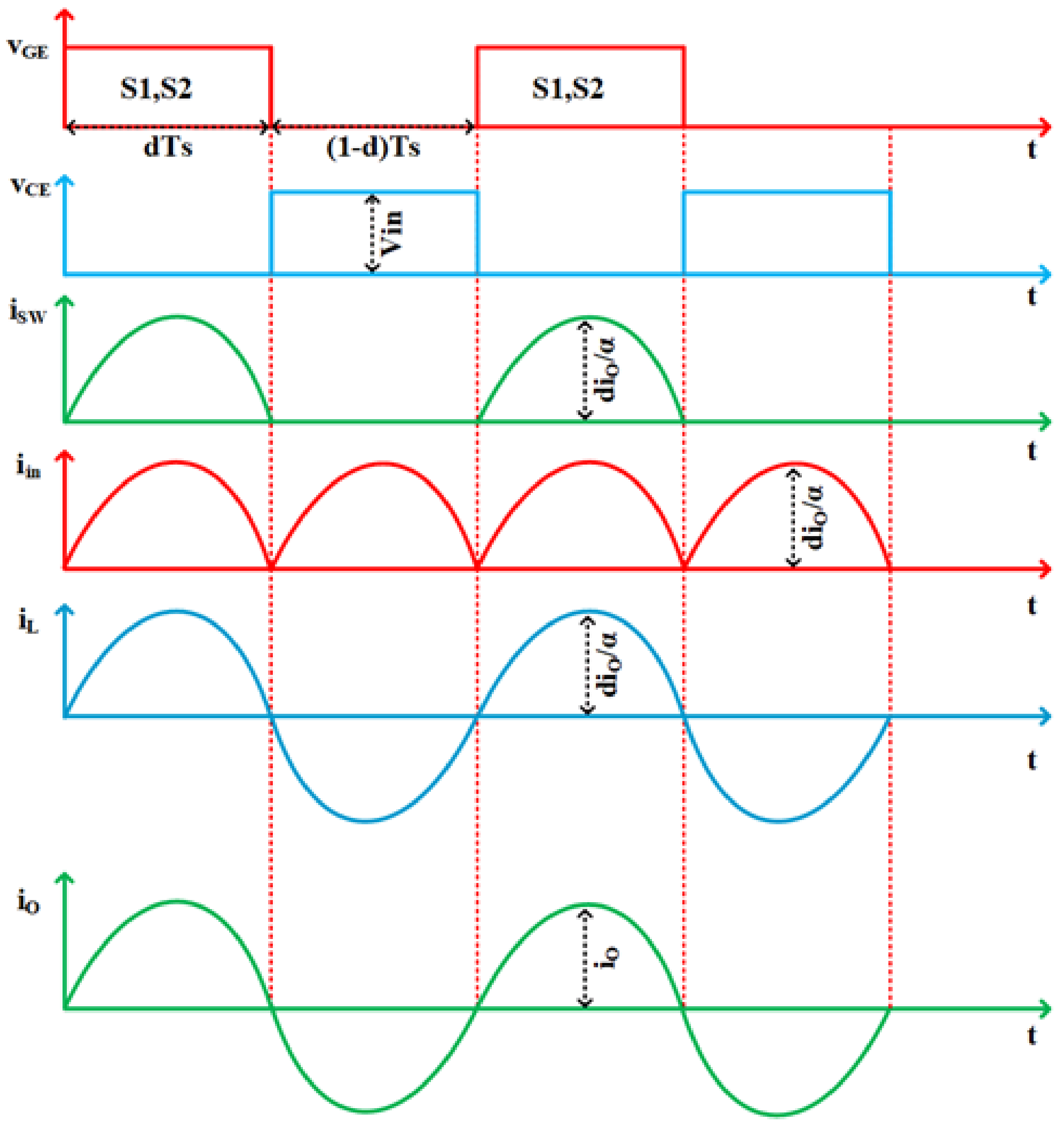
2.1. Steady-State and Dynamic Operation

To explain the operation simply and without any loss of generality, the duty cycle is fixed at fifty percent. In its simplest form, the circuit behaves as a two-pole low pass filter during both modes of operation, as shown in Figure 4.
The transfer function for the circuit is given by:
G s = V o s   V i n s = 1 1 + s L / R + s 2 L C  
where L is inductance, R is load resistance, and C is the capacitance of the circuit. The resonant frequency of the system (ωr) is:
ω r = 1 L C  
Rephrasing Equation (1) in a standard second-order system by substituting ωr from Equation (2), we obtain:
G s = V o s   V i n s = ω r 2 s 2 + α s ω r + ω r 2  
where α = 1 R L C
Now by replacing s by , (3) results in the following Equation:
G j ω = ω r 2 j ω 2 + j ω α ω r + ω r 2  
The gain of the system is given by:
G j ω = 1 ( 1 ω ω r 2 2 + α 2 ω ω r 2  
At the resonant frequency, i.e., ω = ωr Equation (5) gives the value of gain to be 1/α, i.e.;
G j ω = 1 α   = R C L
Equation (6) provides the system’s steady-state gain when the duty cycle is fixed at 0.5. The output voltage across the load is sinusoidal by tuned resonance operation across L and C. The output voltage equation across the load is given by:
V o = V D C α   S i n ω t
However, VDC is a function of input voltage Vin and duty cycle “d” and is given as VDC = d × Vin, which resembles a buck converter’s output voltage, which is evident from the circuit, so that Equation (7) can be rephrased in the form of (8).
V o = d V i n α   S i n ω t
Equation (8) is the dynamic equation of the converter. Considering loss-less components, the power balance of the converter can be given by (9).
| V i n × I i n = V o × I o |
where Vin, Iin is the input voltage and current, and Vo, Io is the output voltage and current, respectively. By substituting VO, from Equation (8), considering maximum value of Sin (ωt) as one, relation between input and output current can be shown as:
I i n = d I o / α
Based on system equations, operational waveforms of circuit operation can be drawn, as shown in Figure 5. The maximum gain of the converter under symmetric operation is achieved at 0.5 duty cycle. For practical quadruple gain of the circuit at 1 kW load, d/α is equal to 4, i.e., d = 0.5 and α = 0.125. The gain for variable load and the variable duty cycle is calculated and plotted in Figure 6.

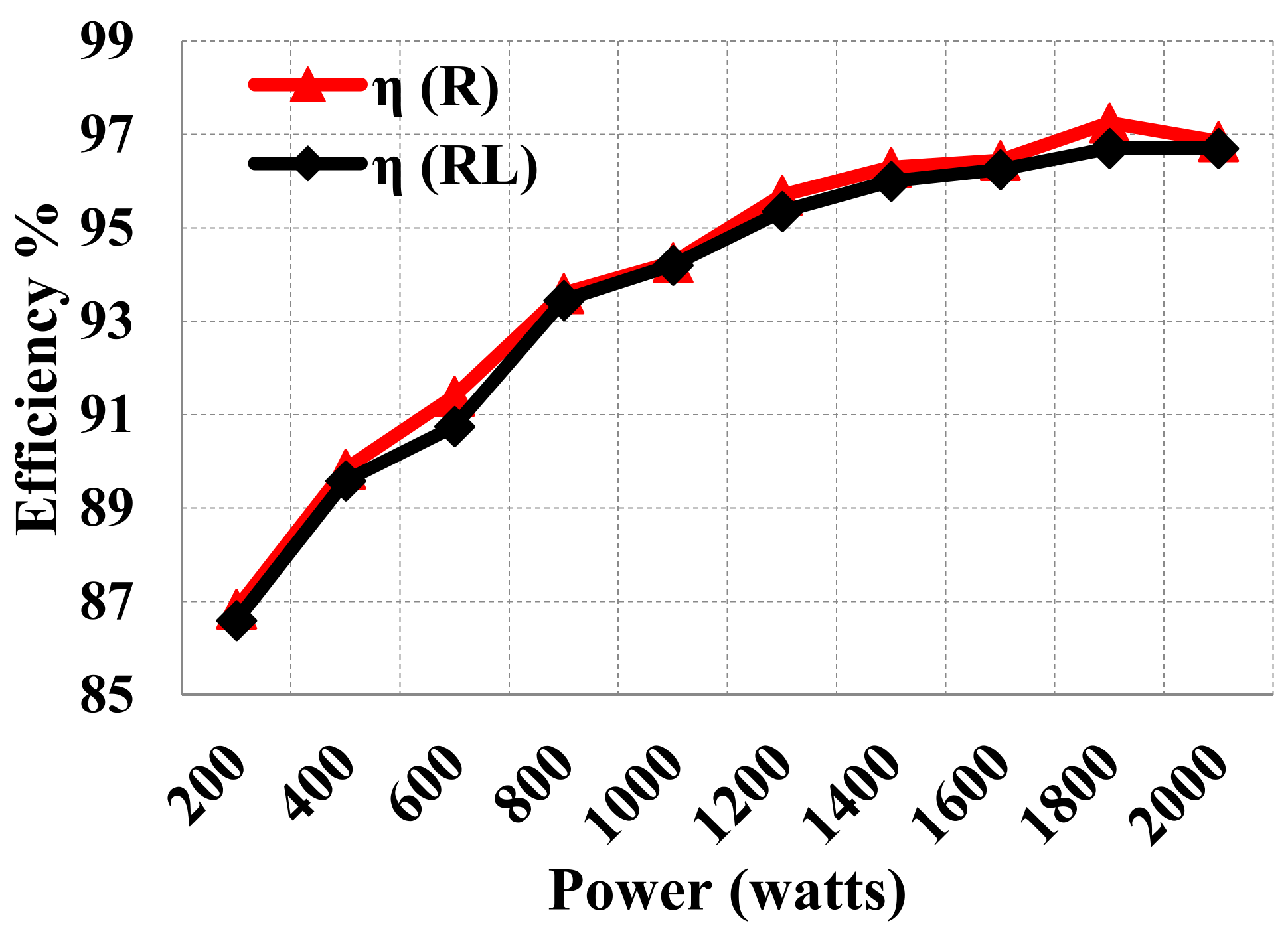
2.2. Loss and Efficiency Calculation

From the operational waveform (see Figure 5), zero current switching of the switches can be observed; the proposed converter has no switching loss associated with it. The conduction loss of the switch (PSWc) with on-time resistance (RCE) is given by:
P S W c = I S W 2 R C E
where ISW is the collector current. As seen from Figure 5, the switch current is half sinusoid; thus, its root mean square (RMS) value is given by:
I S W = d I o / 2 α
Substituting the value of switch current from Equation (12) in Equation (11), switch conduction loss is given by:
P S W c = d I o / 2 α   2 R C E
The current stress on the inductor is a sinusoidal variation with a peak value of dIo/α. Thus, current through inductor responsible for inductor loss is given by (14), i.e.,
I L = d I o / α 2
From (14), inductor loss (PL) is calculated as:
P L = d I o α 2 2   R L
where RL is the DC resistance of the inductor. Another component where the loss occurs in the capacitor due to its equivalent series resistance (ESR). Current through the capacitor is given by:
I C = I L I O
Power loss in the capacitor (PC), with an equivalent series resistance (ESR) is given by:
P C = I C 2   E S R
The efficiency of the converter is given by:
η = P O P O + L o s s e s =     P O P O + P C + P L + P S W
where PO is output power and PC, PL and PSW are capacitor, inductor, and switch losses (as ZCS occurs, switch loss only has conduction loss component).
Based on circuit equations, voltage and current stress across each component can be tabulated as shown in Table 1.
A thermal model of the proposed converter is constructed using PLECS software to verify the calculation efficiency further. The datasheet-assisted thermal model of the switch is shown in Figure 7.

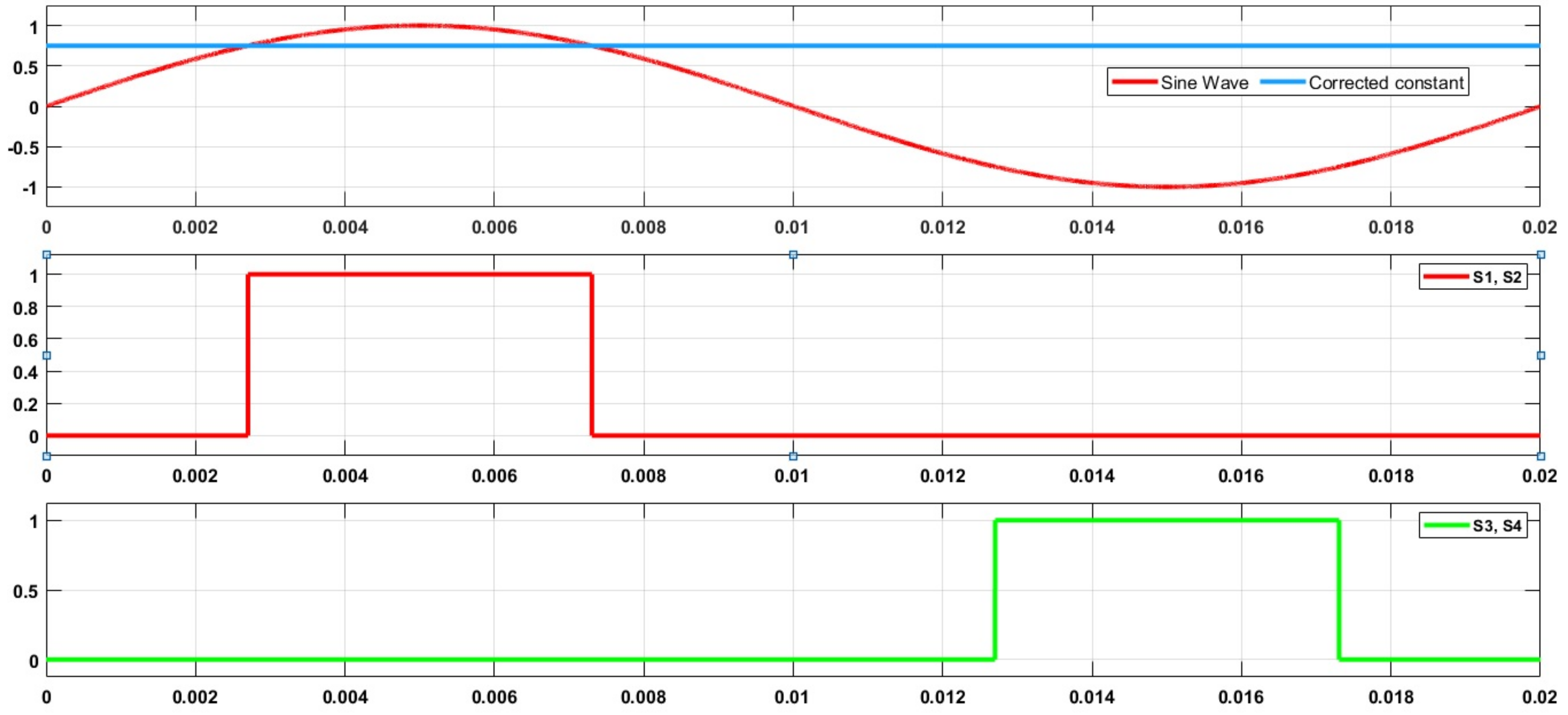
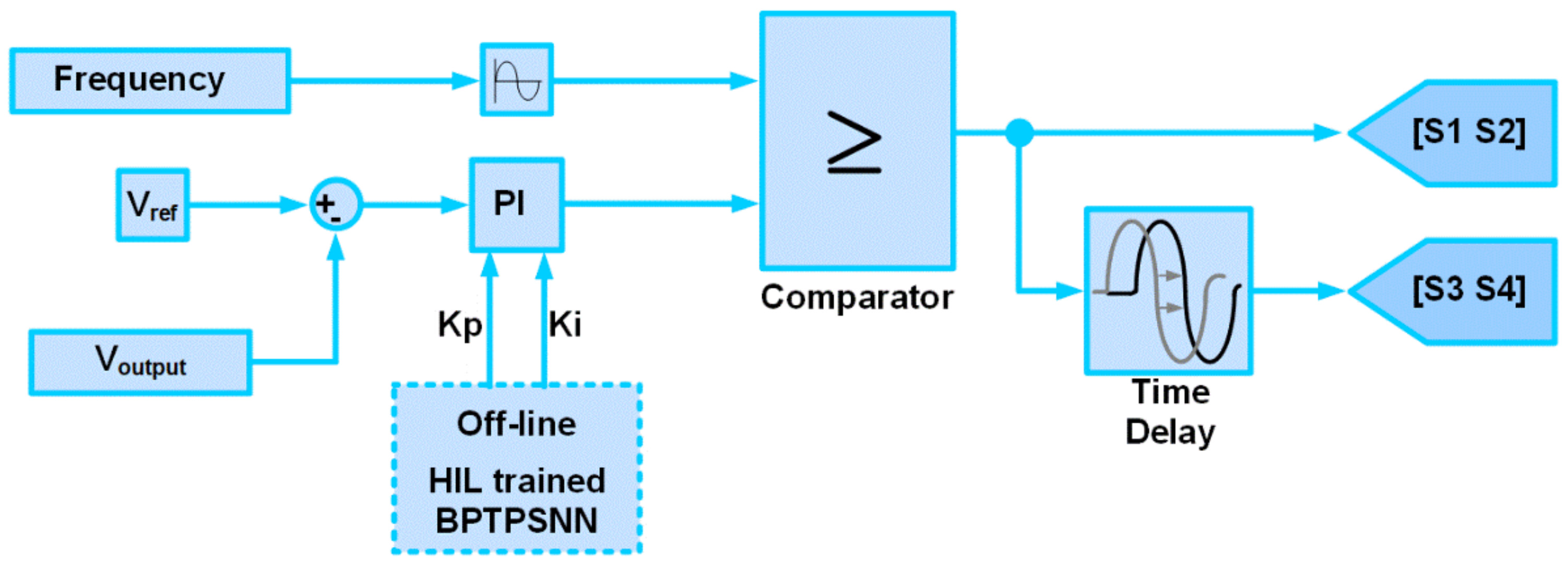
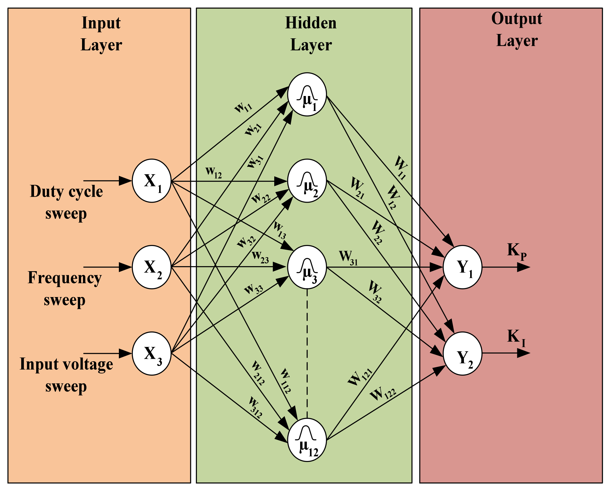
3. Variable Voltage Variable Frequency Controller

Single-stage single-phase boost inverters have the symmetric operation as two converters are working in tandem, so for a proper sinusoidal output waveform generation, the two converters need to be in perfect synchronism.; such converters tend to destabilize above the duty cycle of 0.5, so they are operated in the duty cycle range of 0 to 0.5 [24].
Boost inverters generally employ a sliding mode or close loop waveform controller for symmetric operation at all operation points. The sliding mode controller works only when the sliding surface and tracking equations are accurately defined. In the case of un-optimized functions, chattering is a dominant problem. Finding out the sliding surface and control law equations is a painstaking task and involves two different loops, i.e., inductor current control and capacitor voltage control [35,36] for proper wave-shape tracking, which is sinusoidal in the case of boost inverter.
A new quarter-wave symmetric (QWS) controller has been designed for variable voltage and variable frequency output control. This QWS controller is a Sin cascaded controller in which the frequency of sine wave is changed for variable fundamental frequency operation, and quarter symmetric pulse turn-on time is controlled for variable voltage gain operation. Equation (8) shows that the inverter is capable of variable gain boost factor and variable frequency operation by changing the duty cycle and switching frequency, respectively. The block diagram of the controller is shown in Figure 8. The subsequent pulse generation is also highlighted in Figure 9.
QWS controller produces switching pulses, which vary in frequency and pulse width. Sine cascaded design is applied so as even when the duty cycle varies from 0 to 0.5, they are symmetric at the quarter-wave time. The governing equation for QWS is given by solution from the following simultaneous equations.
y 1 = E K p + K i / s
y 2 = s i n ω t
where ε is the error between Vref and Voutput, Kp and Ki are PI controller gains, and ω is frequency.
For realizing the PI controllers, an online-supervised learning-based artificial neural network is used. A back-propagation thin-plate-spline neural network (BPTPSNN) is utilized using MATLAB Deep Learning Toolbox. For training the network, data are extracted by hardware in the loop setup using OP5130 OPAL-RT. Using the HIL setup, Voutput is recorded for an input voltage sweep, input duty cycle sweep, input modulation sweeps, and input frequency sweep. Therefore, for training the network, known Voutput is available for input frequency, voltage, and duty cycle variation.
BPTPSNN is a feed-forward back-propagation supervised learning neural network based on a thin-plate-spline transfer function [37,38]. The thin-plate-spline function in its simplest form is referred to as radial basis function represented in mathematical form as
y i n = j = 1 H W i j f j u , c , σ
where y i is the output of ith neuron in the hidden layer,   u is input, c is the central value, and σ is variance. W i j is the weighted connection between two different layers. The control signal from the PI controller is expressed in discrete regression terms by:
U k = K p e k + K i T i i = 1 n e i
where e is the error signal, and Ti is the tunable parameters correlated to the weights and bias of the weighted connection in layers. Back-propagation is used for supervised learning as it first adjusts the weighted functions based on the neuron’s activity level, and then back pass is computed based on acquired slope, which reiterates the learning rate. As shown in Figure 10, the input layer is taking the frequency sweep, input voltage sweeps, and duty-cycle perturbation data. This layer computes the maxima and minima range of Kp and Ki values, and the hidden layer optimizes the Kp and Ki values based on readjusted weights and bias, which is transferred to the output layer as optimized gain parameters [38,39]. These PI gain values Kp and Ki are used in real-time implementation of the QWS controller. The Kp and Ki values are saved in the internal registers of the TMS320F28379D for performing the control operation based on voltage feedback and reference requirements.

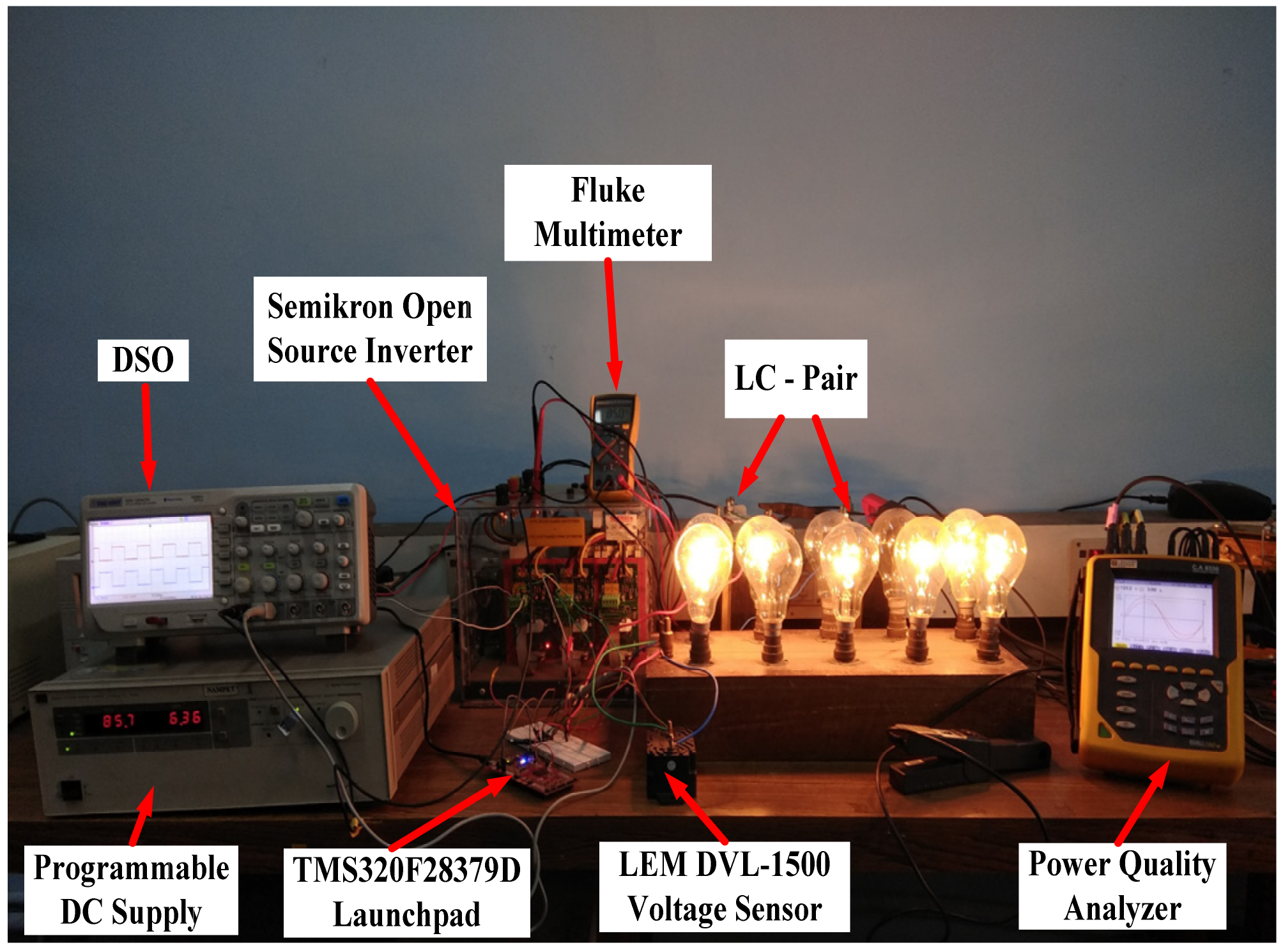
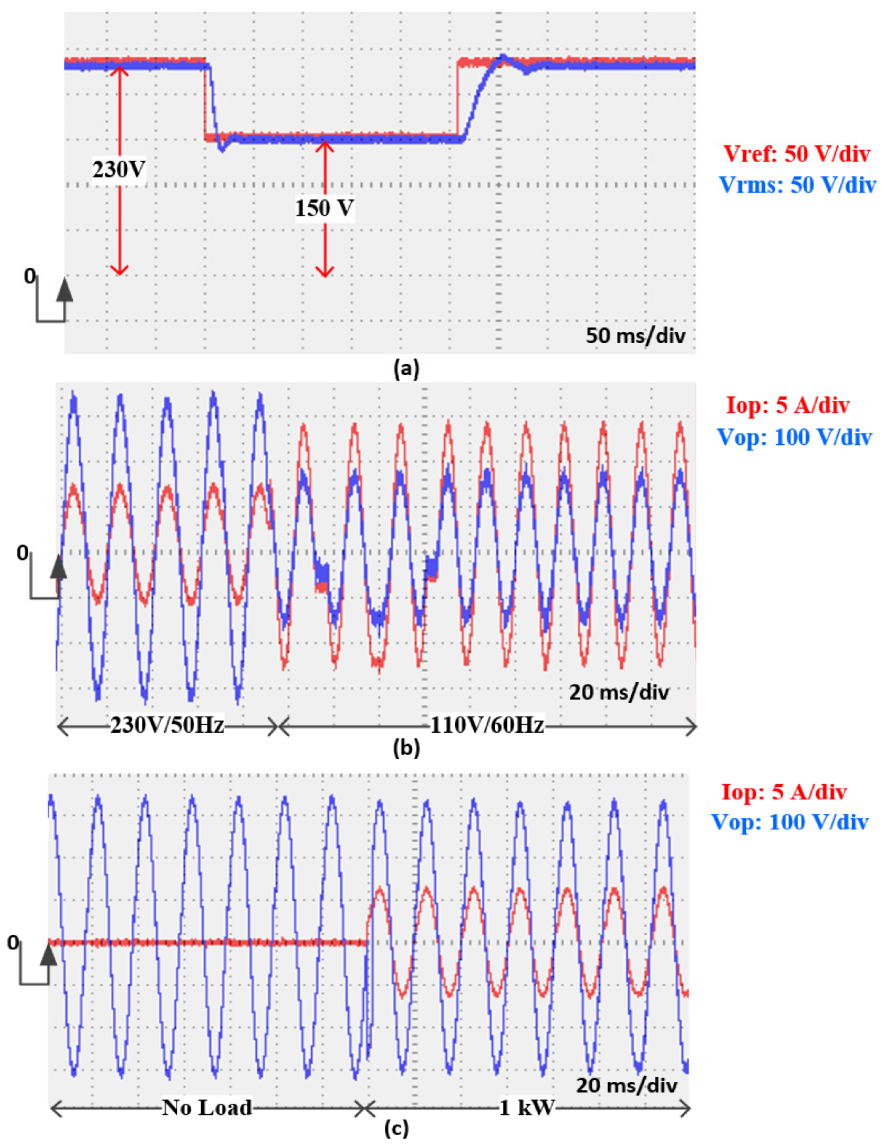
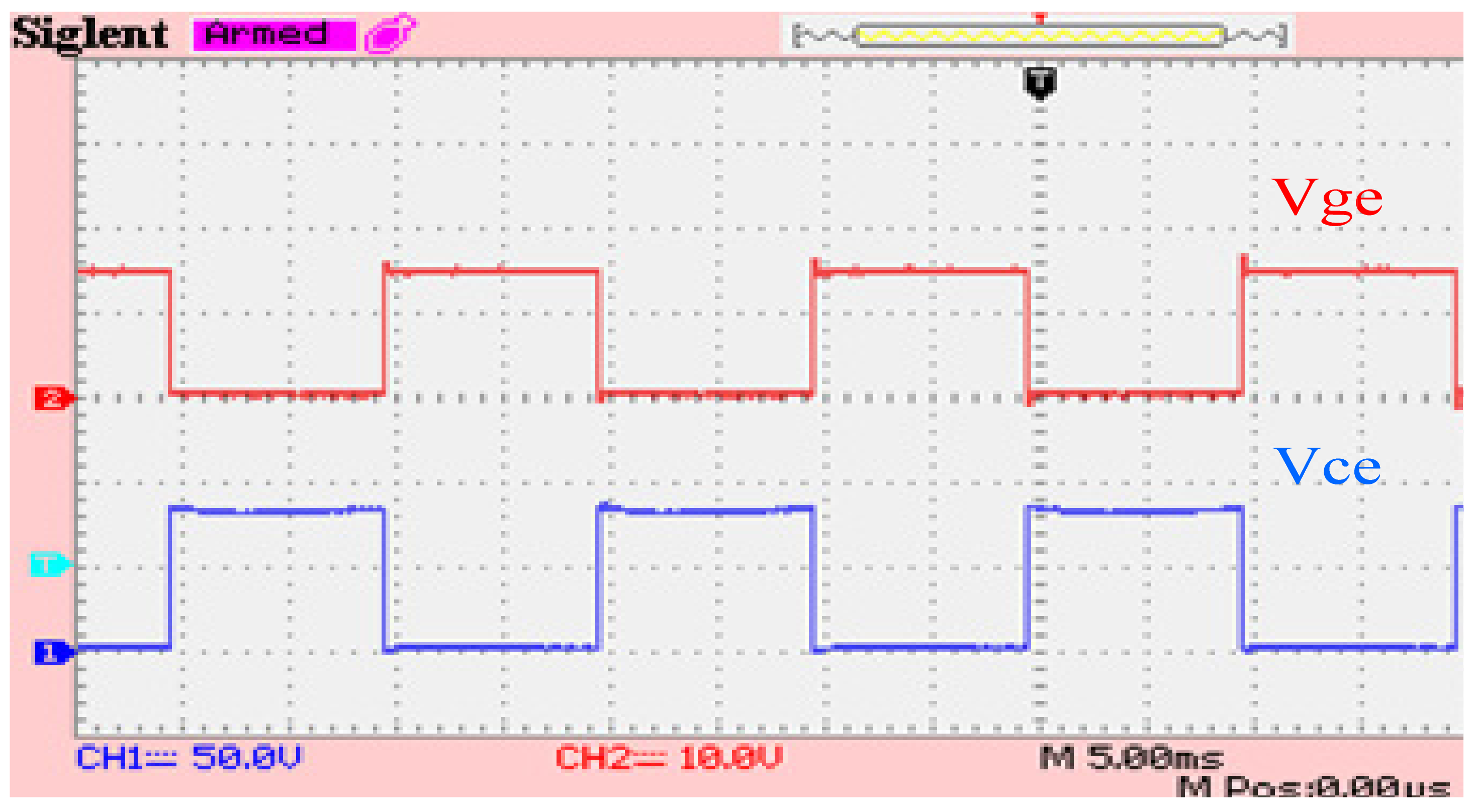
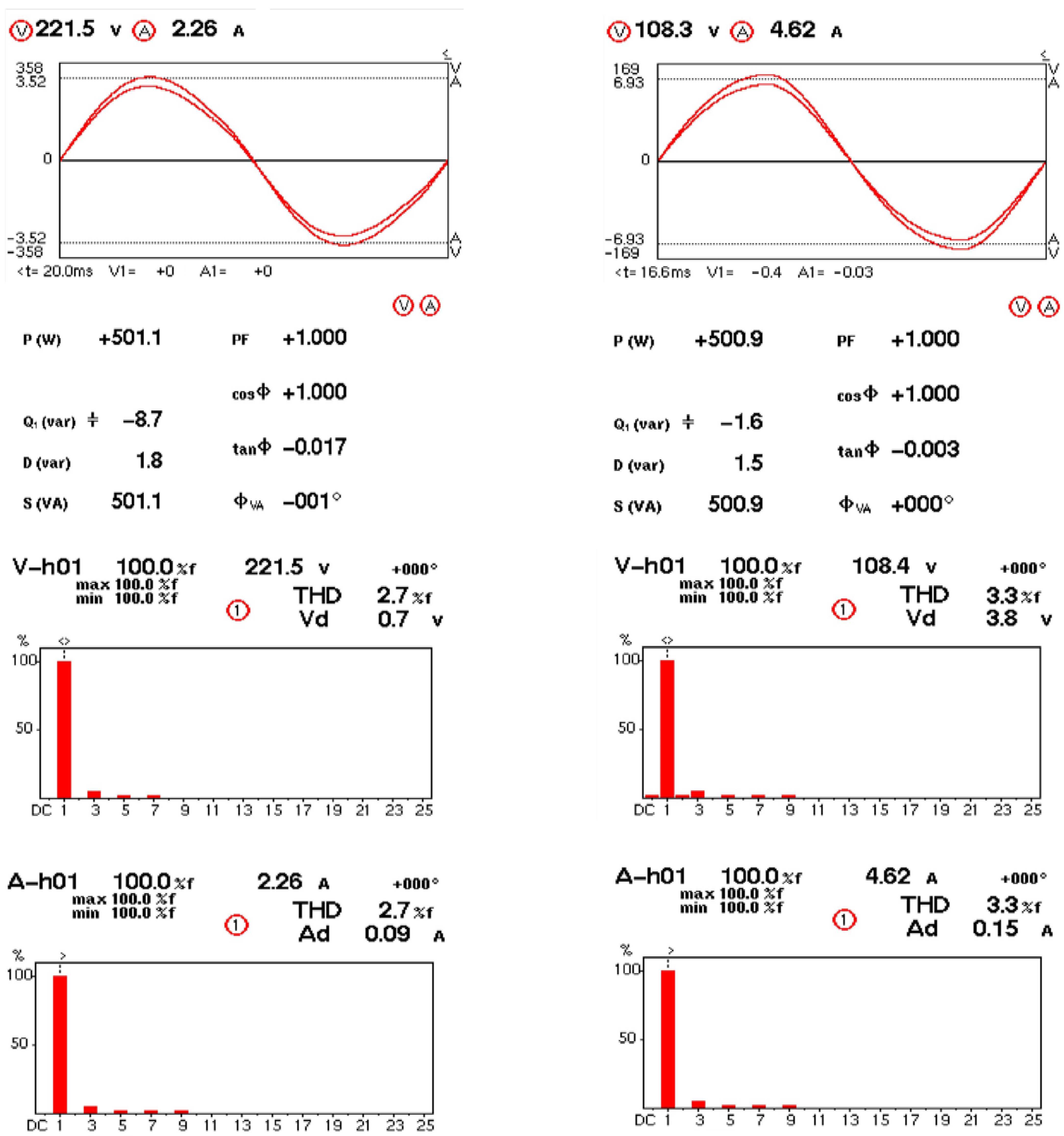
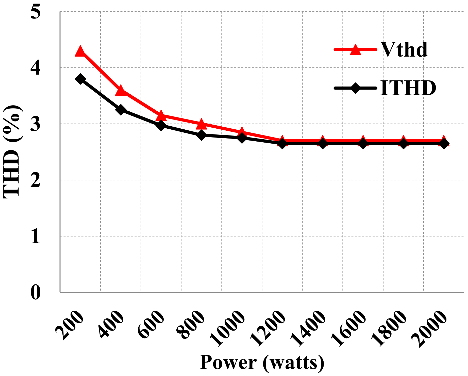
4. Experimental Validation

Experimentation was performed with 2 kW load capability on Semikron open-source inverter module with in-built gate driver and protection circuitry to demonstrate the control system’s effectiveness and the circuit’s capability. LEM DVL–1500 voltage sensor is used for feedback, and the DSP TI TMS320F28379D is used for pulse generation. The experimental setup is shown in Figure 11.
The data recorded in a Chauvin Arnoux power quality analyzer are shown in Figure 12. It can be seen that without any external filter, the inverter can be seamlessly switched from 50 Hz to 60 Hz operation and vice-versa. Unity power factor is maintained as expected from a resistive load in both the operation modes. The voltage and current harmonics for UPF load variation from 200 to 2000 watts is shown in Figure 13. It can be seen that the harmonics at all load levels are well below prescribed THD limits of 5% by IEEE STD-519 [40].
Harmonics present in output voltage and current for different RL loads are reported in Figure 14. These results also conform to the standard requirement of THD limits from a DC/AC inversion system.
The efficiency of the proposed inverter for both resistive and inductive loads is reported in Figure 15. The efficiency of the proposed converter is low at lower loads and increases to an effective value of 97% near full load.
To validate the controller operation, a pulsed reference is applied as Vref, which changes from 230 V to 150 V and then to 230 V, as shown in Figure 16a; it can be seen that Vrms follows Vref faithfully with settling times less than three cycles. The quarter-wave symmetric controller operation for variable voltage and frequency control is validated by switching the output voltage and frequency from 230 V@50 Hz operation to 110 V@60 Hz operation, as shown in Figure 16b. This step-change is introduced with the DC input voltage of 85 volts, showing the controller’s ability to effectively change the output voltage, frequency, and associated gains. For 230 V@50 Hz operation at 85 V, DC input gain is 3.82, while for the 110 V@60 Hz operation, the gain is 1.83. It can be observed that the steady-state has been achieved after step change has been applied within two cycles. Further, the proposed inverter is subjected to a step load of 1 kW from no-load and is illustrated in Figure 16c.
The total blocking voltage (TBV) [41] of the converter is given by:
T B V = i = 1 n P I V i / V o u t p k
where PIV is the peak inverse voltage experienced by each semiconductor device, Voutpk is the peak output voltage, and n denotes the number of semiconductor devices. For the proposed inverter, the PIV of each switch is 85 volts, i.e., equal to DC link voltage, as shown in Figure 17.
The total number of switches is equal to four, and the peak output voltage is 324.7 volts; therefore, TBV of the proposed converter can be given by:
T B V L T Q G B I = 4   ×   85 / 324.7 =   1.05
This low value of TBV signifies lower semiconductor costs as well as loss. A detailed comparative evaluation based on different parameters is shown in Table 2.
When compared with the available designs available in the literature, the superiority of the proposed topology becomes evident. As shown in Table 2, the proposed topology requires fewer components and does not require any filter. This reduces the cost and the losses, is simple, and eases production. Furthermore, this topology achieves more with less as the power level is 4 to 50 times higher than other comparable designs. Finally, operating at kW levels makes this inverter available for different uses, such as battery chargers or electric vehicle domains.

5. Conclusions

The article utilized the conventional H-Bridge-based VSI structure to convert it into a high gain fundamental frequency switched boost inverter capable of converting low voltage DC to required AC voltage in a single stage was proposed in this paper. The proposed converter can have a wide range of applications in renewable energy systems, especially solar-based applications. Further, a variable voltage variable frequency controller was proposed to regulate the load voltage. The proposed controller was effective in regulating the load voltage under disturbances on the source and load intermittencies. The converter was found to have 97% efficiency under full load. A 2-kW laboratory prototype of the proposed converter was developed and found to have the THD levels within the IEEE standards.

Author Contributions

Conceptualization, P.R.T. and V.L.; methodology, P.R.T. and R.K.K.; software, P.R.T. and B.A.; validation, P.R.T. and B.A.; investigation, P.R.T.; resources, P.R.T. and B.A.; data curation, V.L. and R.K.K.; writing—original draft preparation, P.R.T., V.L., and R.K.K.; supervision, T.S.U.; project administration, T.S.U.; formal analysis, T.S.U.; funding acquisition, T.S.U.; visualization, P.R.T.; writing—review and editing: T.S.U. and B.A.; figure and table, P.R.T., V.L. and R.K.K. All authors have read and agreed to the published version of the manuscript.

Funding

This research received no external funding.

Conflicts of Interest

The authors declare no conflict of interest.

References

  1. International Renewable Energy Agency. Global Renewables Outlook: Energy Transformation 2050; International Renewable Energy Agency: Abu Dhabi, United Arab Emirates, 2020; ISBN 978-92-9260-238-3. [Google Scholar]
  2. Javed, K.; Ashfaq, H.; Singh, R.; Hussain, S.M.S.; Ustun, T.S. Design and Performance Analysis of a Stand-alone PV System with Hybrid Energy Storage for Rural India. Electronics 2019, 8, 952. [Google Scholar] [CrossRef] [Green Version]
  3. Ustun, T.S.; Aoto, Y. Analysis of Smart Inverter’s Impact on the Distribution Network Operation. IEEE Access 2019, 7, 9790–9804. [Google Scholar] [CrossRef]
  4. Islam, R.; Mahfuz-Ur-Rahman, A.M.; Muttaqi, K.M.; Sutanto, D. State-of-the-Art of the Medium-Voltage Power Converter Technologies for Grid Integration of Solar Photovoltaic Power Plants. IEEE Trans. Energy Convers. 2019, 34, 372–384. [Google Scholar] [CrossRef]
  5. Jiahui, J.; Yanhui, Q.; Daolian, C. A distributed maximum power point tracking flyback type PV grid-connected inverter. In Proceedings of the IECON 2017—43rd Annual Conference of the IEEE Industrial Electronics Society, Beijing, China, 29 October–1 November 2017; pp. 7713–7717. [Google Scholar]
  6. Samir, A.; Taha, M.; Sayed, M.M.; Ibrahim, A. Efficient PV-grid system integration with PV-voltage-source converter reactive power support. J. Eng. 2018, 2018, 130–137. [Google Scholar] [CrossRef]
  7. Rajeev, M.; Agarwal, V. Single Phase Current Source Inverter with Multiloop Control for Transformerless Grid–PV Interface. IEEE Trans. Ind. Appl. 2018, 54, 2416–2424. [Google Scholar] [CrossRef]
  8. Dash, P.P.; Kazerani, M. Dynamic Modeling and Performance Analysis of a Grid-Connected Current-Source Inverter-Based Photovoltaic System. IEEE Trans. Sustain. Energy 2011, 2, 443–450. [Google Scholar] [CrossRef]
  9. Peng, F.Z. Z-source inverter. IEEE Trans. Ind. Appl. 2003, 39, 504–510. [Google Scholar] [CrossRef]
  10. Ellabban, O.; Abu-Rub, H. Z-Source Inverter: Topology Improvements Review. IEEE Ind. Electron. Mag. 2016, 10, 6–24. [Google Scholar] [CrossRef]
  11. Wang, T.; Nian, H.; Zhu, Z.Q. Using inverter-based renewable generators to improve the grid power quality—A review. Chin. J. Electr. Eng. 2018, 4, 16–25. [Google Scholar] [CrossRef]
  12. Tang, Y.; Xie, S.; Zhang, C.; Xu, Z. Improved Z-Source Inverter with Reduced Z-Source Capacitor Voltage Stress and Soft-Start Capability. IEEE Trans. Power Electron. 2009, 24, 409–415. [Google Scholar] [CrossRef]
  13. Loh, P.C.; Li, D.; Blaabjerg, F. Γ-Z-Source Inverters. IEEE Trans. Power Electron. 2013, 28, 4880–4884. [Google Scholar] [CrossRef]
  14. Cao, D.; Jiang, S.; Yu, X.; Peng, F.Z. Low-Cost Semi-Z-source Inverter for Single-Phase Photovoltaic Systems. IEEE Trans. Power Electron. 2011, 26, 3514–3523. [Google Scholar] [CrossRef]
  15. Ahmad, A.; Singh, R.K.; Beig, B.A. Switched-Capacitor Based Modified Extended High Gain Switched Boost Z-Source Inverters. IEEE Access 2019, 7, 179918–179928. [Google Scholar] [CrossRef]
  16. Tripathi, P.R.; Thakura, P.; Keshri, R.K.; Ghosh, S.; Guerrero, J.M. 25 Years of Single-Stage Buck-Boost Inverters: Development and Challenges. IEEE Ind. Electron. Mag. 2021. [Google Scholar] [CrossRef]
  17. Khenar, M.; Taghvaie, A.; Adabi, J.; Rezanejad, M. Multi-level inverter with combined T-type and cross-connected modules. IET Power Electron. 2018, 11, 1407–1415. [Google Scholar] [CrossRef]
  18. Das, M.K.; Jana, K.C.; Sinha, A. Performance evaluation of an asymmetrical reduced switched multi-level inverter for a grid-connected PV system. IET Renew. Power Gener. 2018, 12, 252–263. [Google Scholar] [CrossRef]
  19. Kumar, N.V.; Chinnaiyan, V.K.; Murukesapillay, P.; Karthikeyan, S.P. Multilevel inverter topology using single source and double source module with reduced power electronic components. J. Eng. 2017, 2017, 139–148. [Google Scholar] [CrossRef]
  20. Samsami, H.; Taheri, A.; Samanbakhsh, R. New bidirectional multilevel inverter topology with staircase cascading for symmetric and asymmetric structures. IET Power Electron. 2017, 10, 1315–1323. [Google Scholar] [CrossRef]
  21. Kim, I.; Chan, R.; Kwak, S. Model predictive control method for CHB multi-level inverter with reduced calculation complexity and fast dynamics. IET Electr. Power Appl. 2017, 11, 784–792. [Google Scholar] [CrossRef]
  22. Salehahari, S.; Babaei, E.; Hosseini, S.H.; Ajami, A. Transformer-based multilevel inverters: Analysis, design and implementation. IET Power Electron. 2019, 12, 1–10. [Google Scholar] [CrossRef]
  23. Caceres, R.; Barbi, I. A boost DC-AC converter: Operation, analysis, control and experimentation. In Proceedings of the IECON’95—21st Annual Conference on IEEE Industrial Electronics, Orlando, FL, USA, 6–10 November 2002; Volume 1, pp. 546–551. [Google Scholar]
  24. Caceres, R.; Barbi, I. A boost DC-AC converter: Analysis, design, and experimentation. IEEE Trans. Power Electron. 1999, 14, 134–141. [Google Scholar] [CrossRef]
  25. Gloire, N.; Lei, D.; Xiaozhong, L.; Furong, X. Single phase grid-connected PV inverter applying a boost coupled inductor. In Proceedings of the 2014 IEEE Conference and Expo Transportation Electrification Asia-Pacific (ITEC Asia-Pacific), Beijing, China, 31 August–3 September 2014; pp. 1–5. [Google Scholar]
  26. Zhang, L.; Ruan, X.; Ren, X. Second-Harmonic Current Reduction for Two-Stage Inverter with Boost-Derived Front-End Converter: Control Schemes and Design Considerations. IEEE Trans. Power Electron. 2018, 33, 6361–6378. [Google Scholar] [CrossRef]
  27. Zhang, L.; Ruan, X. Control Schemes for Reducing Second Harmonic Current in Two-Stage Single-Phase Converter: An Overview From DC-Bus Port-Impedance Characteristics. IEEE Trans. Power Electron. 2019, 34, 10341–10358. [Google Scholar] [CrossRef]
  28. Tran, T.-T.; Nguyen, M.-K.; Choi, J.-H.; Lim, Y.-C. A Single-Phase Common-Ground-Type Boost Inverter for Photovoltaic Applications. In Proceedings of the 2019 21st European Conference on Power Electronics and Applications (EPE ’19 ECCE Europe), Genova, Italy, 3–5 September 2019; pp. 10341–10358. [Google Scholar]
  29. Wu, X.; Zaman, H.; Zheng, X.; Khan, S.; Ali, H. Carrier-Based Double Integral Sliding-Mode Controller of Class-D Amplifier. IEEE Access 2018, 7, 1275–1283. [Google Scholar] [CrossRef]
  30. Jiang, X. Fundamentals of Audio Class D Amplifier Design: A Review of Schemes and Architectures. IEEE Solid-State Circuits Mag. 2017, 9, 14–25. [Google Scholar] [CrossRef]
  31. Chien, S.-H.; Chen, Y.-W.; Kuo, T.-H. A Low Quiescent Current, Low THD+N Class-D Audio Amplifier with Area-Efficient PWM-Residual-Aliasing Reduction. IEEE J. Solid-State Circuits 2018, 53, 3377–3385. [Google Scholar] [CrossRef]
  32. Xu, D.; Zhong, S.; Xu, J. Bipolar Phase Shift Modulation Single-Stage Audio Amplifier Employing a Full Bridge Active Clamp for High Efficiency Low Distortion. IEEE Trans. Ind. Electron. 2021, 68, 1118–1129. [Google Scholar] [CrossRef]
  33. Jain, P. Resonant Power Conversion: Insights from a Lifetime of Experience. IEEE J. Emerg. Sel. Top. Power Electron. 2020. [Google Scholar] [CrossRef]
  34. Kjaer, S.B.; Pedersen, J.K.; Blaabjerg, F. A Review of Single-Phase Grid-Connected Inverters for Photovoltaic Modules. IEEE Trans. Ind. Appl. 2005, 41, 1292–1306. [Google Scholar] [CrossRef]
  35. Abeywardana, D.B.W.; Hredzak, B.; Agelidis, V.G. An Input Current Feedback Method to Mitigate the DC-Side Low-Frequency Ripple Current in a Single-Phase Boost Inverter. IEEE Trans. Power Electron. 2016, 31, 4594–4603. [Google Scholar] [CrossRef]
  36. Jang, M.; Agelidis, V.G. A Minimum Power-Processing-Stage Fuel-Cell Energy System Based on a Boost-Inverter with a Bidirectional Backup Battery Storage. IEEE Trans. Power Electron. 2010, 26, 1568–1577. [Google Scholar] [CrossRef]
  37. Yilmaz, A.S.; Özer, Z. Pitch angle control in wind turbines above the rated wind speed by multi-layer perceptron and radial basis function neural networks. Expert Syst. Appl. 2009, 36, 9767–9775. [Google Scholar] [CrossRef]
  38. Tiwari, R.; Krishnamurthy, K.; Neelakandan, R.B.; Padmanaban, S.; Wheeler, P.W. Neural Network Based Maximum Power Point Tracking Control with Quadratic Boost Converter for PMSG—Wind Energy Conversion System. Electronics 2018, 7, 20. [Google Scholar] [CrossRef] [Green Version]
  39. Şahin, S.; Güzeliş, C. Online Learning ARMA Controllers with Guaranteed Closed-Loop Stability. IEEE Trans. Neural Netw. Learn. Syst. 2015, 27, 2314–2326. [Google Scholar] [CrossRef]
  40. IEEE Recommended Practice and Requirements for Harmonic Control in Electric Power Systems; IEEE Std. 519-2014; IEEE: New York, NY, USA, 2014; pp. 1–29. [CrossRef]
  41. Sandeep, N.; Ali, J.S.M.; Yaragatti, U.R.; Vijayakumar, K. Switched-Capacitor-Based Quadruple-Boost Nine-Level Inverter. IEEE Trans. Power Electron. 2019, 34, 7147–7150. [Google Scholar] [CrossRef]
Figure 1. (a) Half-bridge and (b) full-bridge Class-D amplifier with double-pole filter.
Electronics 10 02499 g001
Figure 2. Circuit of proposed inverter.
Electronics 10 02499 g002
Figure 3. Modes of operation (a) S1, S2 in ON state and (b) S3, S4 in ON state.
Electronics 10 02499 g003
Figure 4. Equivalent circuit in its simplest form.
Electronics 10 02499 g004
Figure 5. Operational waveforms of the proposed inverter.
Electronics 10 02499 g005
Figure 6. Gain variation with the duty cycle for fixed DC link voltage and on different loads.
Electronics 10 02499 g006
Figure 7. Turn-on energy, turn-off energy, and conduction loss variation (from top to bottom, respectively).
Electronics 10 02499 g007
Figure 8. Functional diagram of the QWS controller.
Electronics 10 02499 g008
Figure 9. Phase-shifted pulse generation from the QWS controller.
Electronics 10 02499 g009
Figure 10. Layers and weighted connection of proposed BPTPSNN.
Electronics 10 02499 g010
Figure 11. Experimental setup.
Electronics 10 02499 g011
Figure 12. (Top to bottom) output voltage and current waveform, power and PF, voltage THD, and current THD, respectively. Left for 50Hz operation, right for 60 Hz operation.
Electronics 10 02499 g012
Figure 13. THD at various UPF load levels.
Electronics 10 02499 g013
Figure 14. Voltage and current harmonics at various RL load.
Electronics 10 02499 g014
Figure 15. Experimental power conversion efficacy of inverter.
Electronics 10 02499 g015
Figure 16. (a) Pulse voltage change response of the controller. (b) Fixed load voltage and frequency control response. (c) No-load to half rated load step change response.
Electronics 10 02499 g016
Figure 17. Gating signal VGE = 15 Volts and switch voltage VCE = 85 volts.
Electronics 10 02499 g017
Table 1. Voltage and current stress.
ComponentVoltage StressCurrent Stress
SwitchdVindIo/2α
Inductor-dIo/2α
CapacitorVoIodIo/√2α
Table 2. Comparative evaluation.
TopologyNsNDNLNCFilterPower Level
[5]6222Yes500 W
[7]4422Yes250 W
[14]2022Yes40 W
[17]29008NO265 W
[26]5412Yes343 W
Proposed4011NO2000 W
Publisher’s Note: MDPI stays neutral with regard to jurisdictional claims in published maps and institutional affiliations.

