


An Overview of Substrate Copper Trace Crack Through Experiments, Characterization, and Numerical Simulations
 , , and
Abstract
1. Introduction
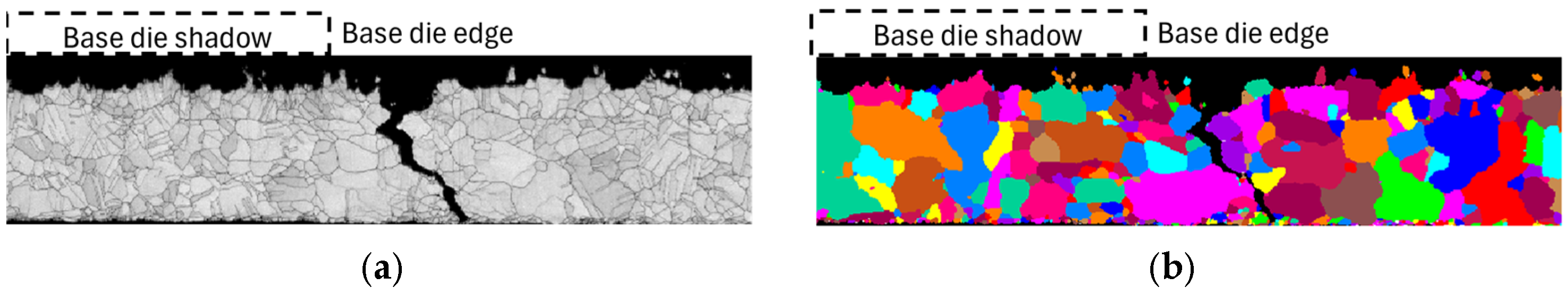
2. Experimental Observations
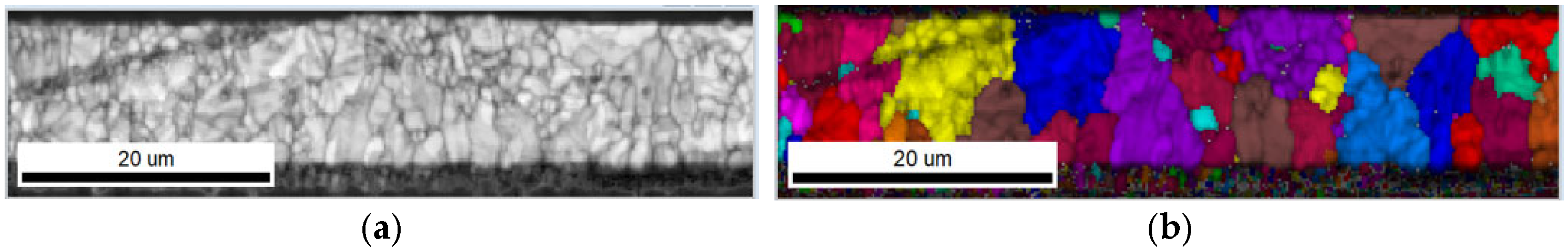
3. Copper Foil Characterization
3.1. Sample Preparation
3.2. Testing Methodology
3.3. Results and Discussion
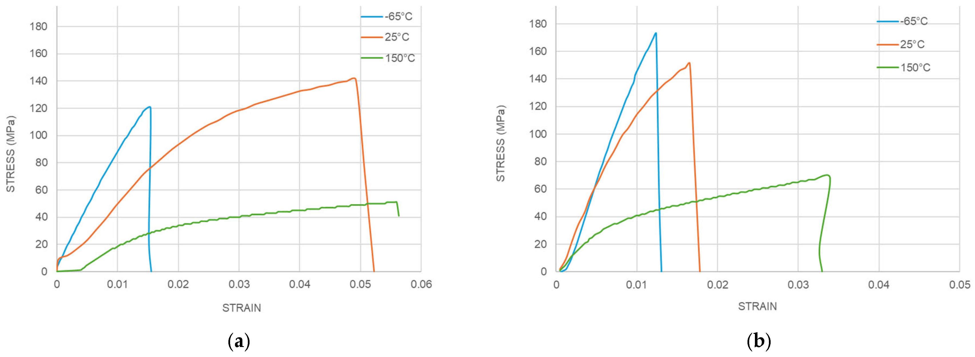
3.3.1. DMA Stress–Strain Tensile Test
3.3.2. DMA Temperature Sweep Test
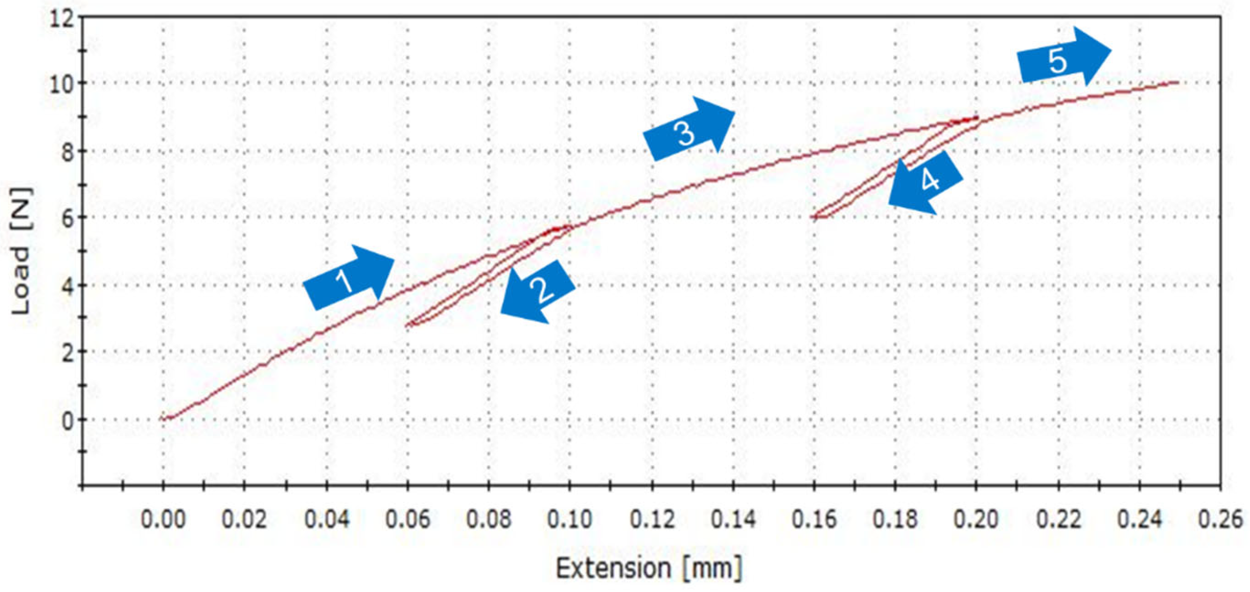
3.3.3. Loading—Unloading Test
3.3.4. Nanoindentation Test
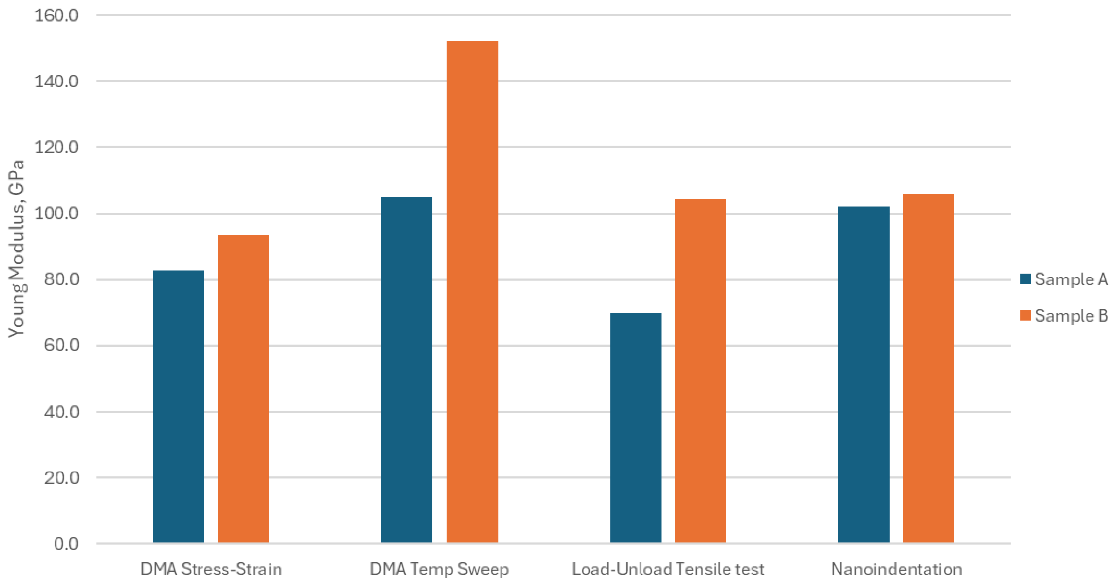
3.3.5. Modulus Comparison
4. Numerical Simulation
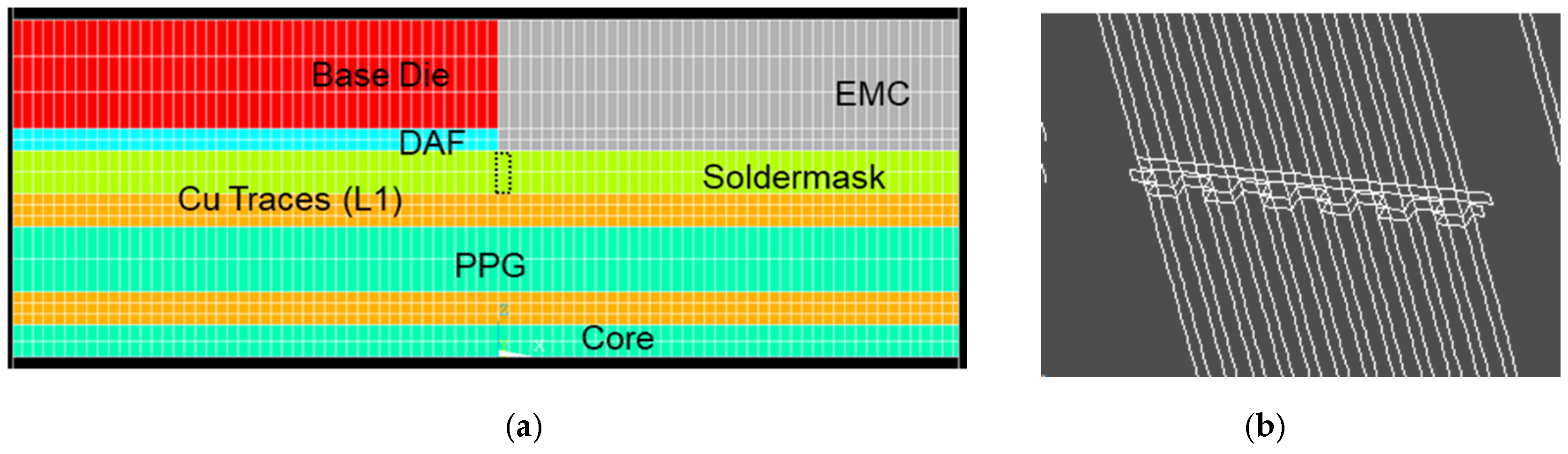
4.1. Modeling Methodology and Results
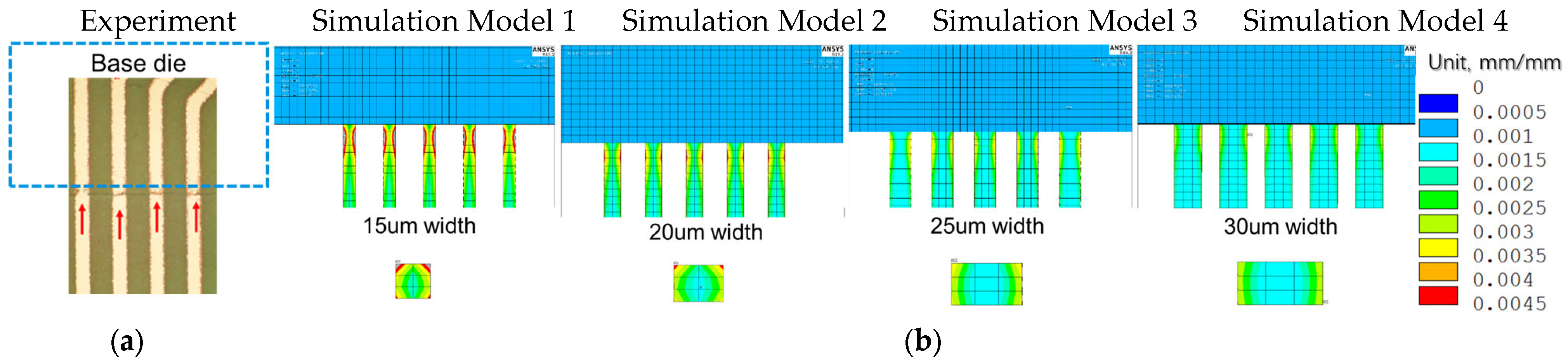
4.2. Effect of Trace Dimension
4.3. Effect of Copper Plasticity
4.4. Effect of SR Type
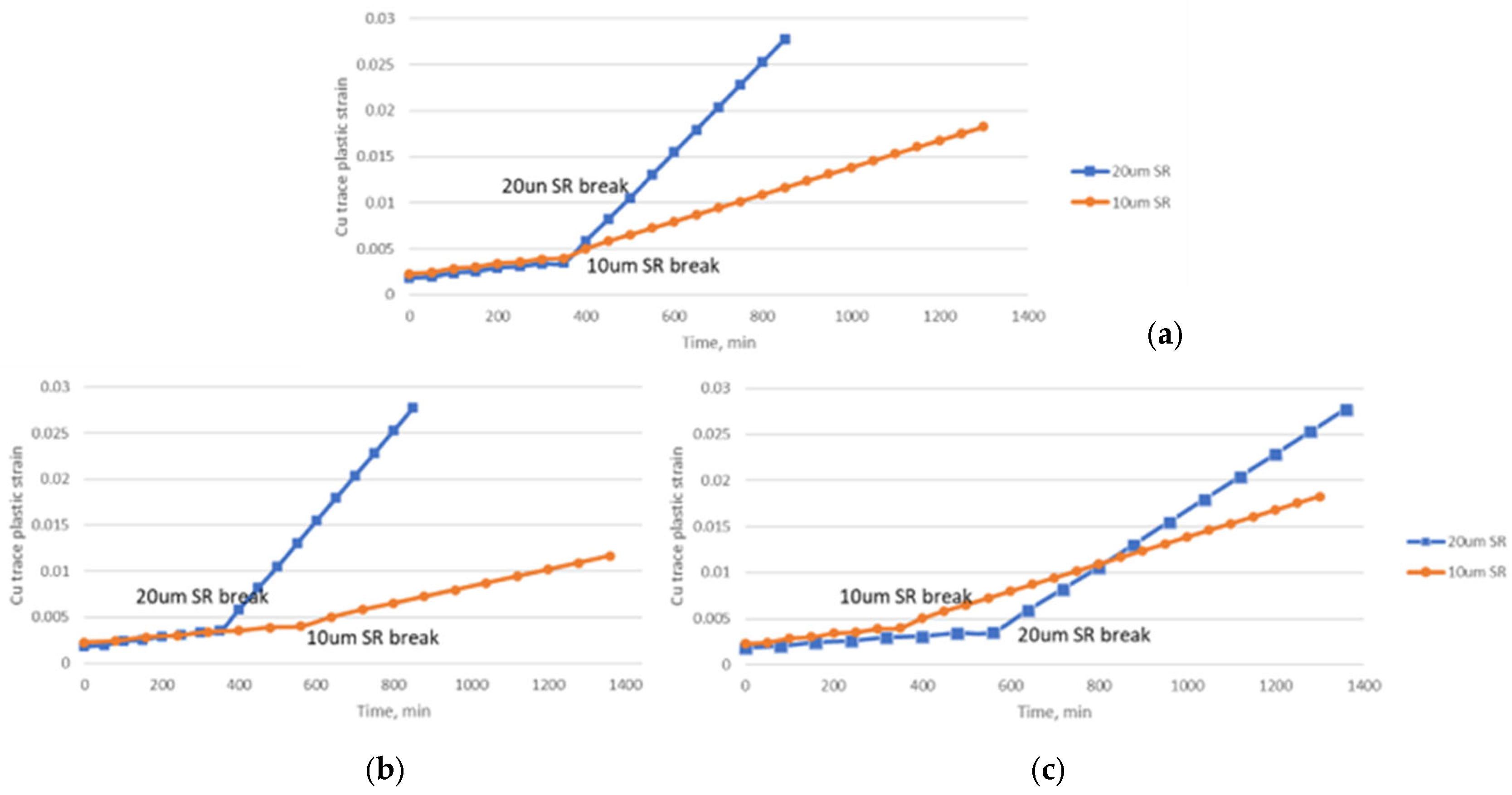
4.5. Effect of SR Breaks
- Model 1: This model represents the scenario when the SR layer is intact, with all elements being properly connected to each other.
- Model 2: This model simulates the damaged SR layer, where the copper trace is exposed and unprotected at the base die edge. This is achieved using the element kill function to deactivate a row of SR elements at the base die edge, on top of and surrounding the Cu traces, like a comb structure in Figure 10.
5. Conclusions
6. Future Work
Author Contributions
Funding
Data Availability Statement
Acknowledgments
Conflicts of Interest
References
- Weiss, B.; Groger, V.; Khatibi, G.; Kotas, A.; Zimprich, P.; Stickler, R.; Zagar, B. Characterization of mechanical and thermal properties of thin Cu foils and wires. Sens. Actuators A 2002, 99, 172–182. [Google Scholar] [CrossRef]
- Li, Y.; Huang, G.; Yin, X.; Chen, X.; Ma, X.; Li, Y.; Yao, E. Effect of Copper Ion Concentration on Microstructure and Mechanical Properties of Electrolytic Copper Foil. IOP Conf. Ser. Mater. Sci. Eng. 2018, 381, 012166. [Google Scholar]
- Wunderle, B.; May, D.; Zschenderlein, U.; Ecke, R.; Springborn, M.; Jöhrmann, N.; Pareek, K.A.; Heilmann, J.; Stiebing, M.; Arnold, J.; et al. Thermo-mechanical Characterisation of Thin Sputtered Copper Films on Silicon: Towards Elasto-Plastic, Fatigue and Subcritical Fracture-Mechanical Data. In Proceedings of the 2018 19th International Conference on Thermal, Mechanical and Multi-Physics Simulation and Experiments in Microelectronics and Microsystems (EuroSimE), Toulouse, France, 15–18 April 2018. [Google Scholar]
- Espinosa, H.D.; Prorok, B.C.; Fischer, M. A methodology for determining mechanical properties of freestanding thin films and MEMS materials. J. Mech. Phys. Solids 2003, 51, 47–67. [Google Scholar]
- Zhang, G.P.; Zhu, X.F.; Li, Y.P. Evaluation of Reliability of Metal Films/Multilayers. In Proceedings of the 10th Electronics Packaging Technology Conference, Singapore, 9–12 December 2008; pp. 890–896. [Google Scholar]
- Beck, D.; Thayer, G.; Sorensen, N.; Susan, D. Fatigue behavior of thin Cu foils and Cu/Kapton flexible circuits. In Proceedings of the Materials Science and Technology Conference and Exhibition, Pittsburgh, PA, USA, 6–9 October 2008. [Google Scholar]
- Zhang, S.; Sakane, M.; Nagasawa, T.; Kobayashi, K. Mechanical properties of copper thin films used in electronic devices. Procedia Eng. 2011, 10, 1497–1502. [Google Scholar] [CrossRef]
- Li, G.; Thomas, B.G.; Stubbins, J.F. Modeling creep and fatigue of copper alloys. Metallurg. Mater. Trans. A 2000, 31, 2491–2502. [Google Scholar]
- Che, F.X.; Putra, W.N.; Heryanto, A.; Trigg, A.; Zhang, X.W.; Gan, C.L. Study on Cu Protrusion of Through-Silicon Via (TSV). IEEE Trans. Compon. Packag. Manuf. Technol. 2013, 3, 732–739. [Google Scholar] [CrossRef]
- Yu, W.; Che, F.X.; Ong, Y.C.; Ng, H.W. Study on Substrate Crack through Experiment and Simulation on SSD BGA under Temperature Cycling. In Proceedings of the 24th Electronics Packaging Technology Conference, Singapore, 7–9 December 2022; pp. 694–698. [Google Scholar]
- Yu, W.; Che, F.X.; Ong, Y.C.; Pan, L.; Cheong, W.G. Study on Substrate Cu Pad Crack through Experiment and Simulation. In Proceedings of the 26th Electronics Packaging Technology Conference, Singapore, 3–6 December 2024; pp. 917–922. [Google Scholar]
- Liu, Y.; Yang, B.; Huang, S.; Ye, N.; Bhagath, S.; Shukla, R. Board level reliability enhancement with considerations of solder ball, substrate and PCB. In Proceedings of the 70th Electronic Components and Technology Conference, Orlando, FL, USA, 3–30 June 2020; pp. 249–256. [Google Scholar]
- Yu, W.; Che, F.X.; Liu, V.; Lin, J.; Rumsey, B.; Ong, Y.C.; Ng, H.W. Substrate Copper Trace Crack Characterization and Simulation. In Proceedings of the 73rd Electronic Components and Technology Conference, Orlando, FL, USA, 30 May–2 June 2023; pp. 699–705. [Google Scholar]
- Abbas, S.M.; Yu, Q.; Pecht, M. Influence of substrate on microvia structures in printed circuit boards during reflow. IEEE Access 2023, 11, 142487–142494. [Google Scholar]
- Yu, W.; Pan, L.; Tan, K.; Che, F.X.; Ong, Y.C.; Ng, H.W. Effect of Underfill on Substrate Trace Crack under PTC. In Proceedings of the 25th Electronics Packaging Technology Conference, Singapore, 5–8 December 2023; pp. 678–682. [Google Scholar]
- Yuan, Y.; Carpenter, B.J. Trace crack in molded thin substrate package, root causes and FEM modeling. In Proceedings of the 5th International Conference on Electronic Packaging Technology, Shanghai, China, 28–30 October 2003; pp. 449–454. [Google Scholar]
- Muniandy, K.V.C.; Jin, C.K.; Peter, J.L. Solder Resist Crack Resistance Process Characterization in BGA Package for Automotive Grade Reliability. In Proceedings of the 20th Electronics Packaging Technology Conference, Singapore, 4–7 December 2018; pp. 120–124. [Google Scholar]
- Jasmine, L.; Tu-Anh, T.; Sandeep, S.; Koh, W. Package Design Characterization Influencing Substrate Metal Crack in BGA Package. In Proceedings of the 25th Electronics Packaging Technology Conference, Singapore, 5–8 December 2023; pp. 169–176. [Google Scholar]
- ASTM E345-16; Standard Test Methods of Tension Testing of Metallic Foil. ASTM International: West Conshohocken, PA, USA, 2016.
- Smith, W.F.; Hashemi, J. Foundations of Material Science and Engineering, 4th ed.; McGraw-Hill: New York, NY, USA, 2006; p. 242. [Google Scholar]
- Trost, C.O.W.; Wurster, S.; Freitag, C.; Steinberger, A.; Cordill, M.J. A new approach to evaluate the elastic modulus of metallic foils. Mater. Des. 2020, 196, 109149. [Google Scholar] [CrossRef]
- Lawn, B.R.; Evans, A.G.; Marshall, D.B. Elastic/Plastic Indentation Damage in Ceramics: The Median/Radial Crack System. J. Am. Ceram. Soc. 1980, 63, 574–581. [Google Scholar] [CrossRef]
- Amiri, S.; Chen, X.; Manes, A.; Giglio, M. An analysis of copper film mechanical properties by means of nanoindentation technique. In Proceedings of the 2014 IEEE 9th Nanotechnology Materials and Devices Conference, Aci Castello, Italy, 12–15 October 2014. [Google Scholar]
- Coffin, L.F. A study of the effects of cyclic thermal stresses on a ductile metal. Trans. ASME 1954, 76, 931–950. [Google Scholar]
- Manson, S.S. Behavior of materials under conditions of thermal stress. In Heat Transfer Symposium; University of Michigan: Ann Arbor, MI, USA, 1953. [Google Scholar]
- Chen, R.; Chow, J.; Sitaraman, S.K. Damage Evolution of Double-Sided Copper Conductor on Multi-layer Flexible Substrate Under Bending. In Proceedings of the 72nd Electronic Components and Technology Conference, San Diego, CA, USA, 31 May–3 June 2022; pp. 729–738. [Google Scholar]
- Darveaux, R. Effect of simulation methodology on solder joint crack growth correlation. In Proceedings of the 50th Electronic Components and Technology Conference, Las Vegas, NV, USA, 21–24 May 2000; pp. 1048–1058. [Google Scholar]


| Failure Modes | A | B1 | B2 | C |
|---|---|---|---|---|
| Schematic |  | 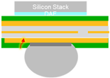 |  |  |
| SEM Images | 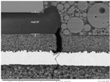 | 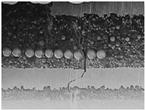 | 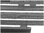 | 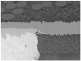 |
| Initiation | Top solder resist (SR) | Bottom SR | Bottom SR | IMC/Cu interface |
| Propagation | SR ⟶ Cu | SR ⟶ Cu | SR ⟶ PPG ⟶ Cu | IMC ⟶ Cu |
| Location (Z) | Primary | Secondary layer | Inner layer or primary layer | Secondary layer |
| Location (XY) | Base die edge | Die edge/shadow | Die edge/shadow | Die shadow |
| Sample A | Sample B | |
|---|---|---|
| Supplier | A | B |
| ED copper foil thickness, µm | 1.5 | 2 |
| Electrolytic-plated copper thickness, µm | 13.5 | 13 |
| Total copper sample thickness, µm | 15 | 15 |
| Annealing temperature | 190 °C | 150 °C |
| Test Method | Sample Dimension | Test Temperature | Test Condition | Sample Size | |
|---|---|---|---|---|---|
| 1 | Tensile Stress–Strain | 3 × 10 mm | −65 °C, 30 °C, 150 °C | 0.02%/s | 3 |
| 2 | Tensile Temperature Sweep | 3 × 10 mm | −65 °C~260 °C | 3 °C/min, 1 Hz | 3 |
| 3 | Tensile Loading–Unloading | 3 × 50 mm | −65 °C, 30 °C, 150 °C | 0.2%/s | 3 |
| 4 | Nanoindentation | - | 30 °C | 300 nm depth | 16 |
| Young’s Modulus, GPa | −65 °C | 30 °C | 150 °C |
|---|---|---|---|
| Sample A | 90.0 | 82.6 | 60.2 |
| Sample B | 106.2 | 93.5 | 90.8 |
| Storage Modulus, GPa | −65 °C | 30 °C | 150 °C |
|---|---|---|---|
| Sample A | 111 | 105 | 89 |
| Sample B | 161 | 152 | 132 |
| Young’s Modulus, GPa | −65 °C | 30 °C | 150 °C |
|---|---|---|---|
| Sample A | 63 | 70 | 66 |
| Sample B | 87 | 104 | 96 |
| Young’s Modulus (E), GPa | Hardness (H), GPa | E/H | |
|---|---|---|---|
| Sample A | 101 ± 3.5 | 1.37 ± 0.09 | 74 |
| Sample B | 106 ± 2.9 | 1.73 ± 0.08 | 61 |
| Failure Mode | A | B | C |
|---|---|---|---|
| Experimental Results | 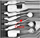 |  |  |
| Simulation Results | 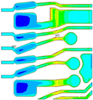 | 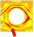 | 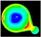 |
| Model | 1 | 2 | 3 | 4 |
|---|---|---|---|---|
| Trace Width, µm | 15 | 20 | 25 | 30 |
| Trace Thickness, µm | 15 | 15 | 15 | 15 |
| Relative Cu Plastic Strain | 127% | 109% | 100% | 87% |
| Model 4 | Model 2a | Model 2b | |
|---|---|---|---|
| Supplier A: actual case | Supplier B: actual case | ||
| Measured trace width, µm | 30 | 20 | 20 |
| Measured trace thickness, µm | 15 | 13 | 13 |
| Cross-sectional area, µm2 | 450 | 260 | 260 |
| Stress–strain input | Supplier A | Supplier A | Supplier B |
| Relative Vol. Ave. plastic strain (simulation) | 100% | 122% | 152% |
| TC-C 1000 cycles results (experiment) | Pass | - | Fail |
| Design A with SR Type 1 | Design B with SR Type 2 | |||
|---|---|---|---|---|
| Simulation Response | Failure mode A | Stress on the top SR | 100% | 66% |
| Strain on the top Cu trace | 100% | 25% | ||
| Failure mode B2 | Stress on the bottom SR | 100% | 67% | |
| Strain on the inner Cu trace | 100% | 97% | ||
| Experiment Failure Rate | Failure mode A | TC-C 2000 cycles | 80/240 | 25/240 |
| Failure mode B2 | TC-C 1000 cycles | 20/79 | 0/79 |
Disclaimer/Publisher’s Note: The statements, opinions and data contained in all publications are solely those of the individual author(s) and contributor(s) and not of MDPI and/or the editor(s). MDPI and/or the editor(s) disclaim responsibility for any injury to people or property resulting from any ideas, methods, instructions or products referred to in the content. |
© 2025 by the authors. Licensee MDPI, Basel, Switzerland. This article is an open access article distributed under the terms and conditions of the Creative Commons Attribution (CC BY) license (https://creativecommons.org/licenses/by/4.0/).
Share and Cite
Yu, W.; Che, F.; Liu, V.; Chen, R.; Ireland, S.; Ong, Y.C.; Ng, H.W.; Kumar, G. An Overview of Substrate Copper Trace Crack Through Experiments, Characterization, and Numerical Simulations. Micromachines 2025, 16, 428. https://doi.org/10.3390/mi16040428
Yu W, Che F, Liu V, Chen R, Ireland S, Ong YC, Ng HW, Kumar G. An Overview of Substrate Copper Trace Crack Through Experiments, Characterization, and Numerical Simulations. Micromachines. 2025; 16(4):428. https://doi.org/10.3390/mi16040428
Chicago/Turabian StyleYu, Wei, Faxing Che, Vance Liu, Raymond Chen, Sam Ireland, Yeow Chon Ong, Hong Wan Ng, and Gokul Kumar. 2025. "An Overview of Substrate Copper Trace Crack Through Experiments, Characterization, and Numerical Simulations" Micromachines 16, no. 4: 428. https://doi.org/10.3390/mi16040428
APA StyleYu, W., Che, F., Liu, V., Chen, R., Ireland, S., Ong, Y. C., Ng, H. W., & Kumar, G. (2025). An Overview of Substrate Copper Trace Crack Through Experiments, Characterization, and Numerical Simulations. Micromachines, 16(4), 428. https://doi.org/10.3390/mi16040428