Abstract
This work systematically investigates the heteroepitaxial growth of β-Ga2O3 thin films under varied substrate and temperature conditions via metalorganic chemical vapor deposition (MOCVD). Comprehensive characterization reveals that both the substrate type and growth temperature significantly influence the crystalline quality, surface morphology, chemical composition, and defect structure. Films grown at higher temperatures generally exhibit superior crystallinity and closer-to-stoichiometry composition, and thus suggest a reduction in oxygen deficiency. Certain substrates are shown to facilitate high-quality epitaxial growth with smooth surfaces and excellent crystallographic alignment. These findings offer key insights into optimizing growth parameters for high-performance β-Ga2O3-based devices.
1. Introduction
Beta-gallium oxide (β-Ga2O3) is an emerging ultra-wide-bandgap (~4.9 eV) semiconductor with a high critical electric field (~8 MV/cm) and excellent thermal and chemical stability [1,2,3,4,5]. These properties make it a promising candidate for high-power electronic devices, solar-blind photodetectors, and extreme-environment applications [6,7,8,9,10]. However, the development of β-Ga2O3-based technology is hampered by the high cost and small wafer size of commercially available native substrates, driving significant interest in heteroepitaxial growth on compatible foreign substrates [11,12,13,14,15].
Heteroepitaxy of β-Ga2O3, however, faces fundamental challenges, primarily due to lattice and thermal expansion mismatch between the film and substrate. These mismatches often lead to high defect densities, residual stress, and degraded electronic performance. In particular, oxygen vacancies—the dominant native point defect in β-Ga2O3—play a decisive role in controlling electrical conductivity, affecting device performance and stability [16,17,18]. Therefore, understanding and controlling the formation of oxygen vacancies during heteroepitaxy is crucial for tailoring the material’s electronic properties.
To address these challenges, this work systematically investigates the heteroepitaxial growth of β-Ga2O3 films on five different substrates—sapphire with 0°, 1.5°, and 6° off-cut angles, p-GaN/sapphire, and AlN/sapphire—at two representative temperatures (400 °C and 800 °C) using MOCVD. The influence of substrate type and growth temperature on the crystal structure, surface morphology, stress state, oxygen non-stoichiometry, and defect content is thoroughly examined using high-resolution X-ray diffraction (XRD), atomic force microscopy (AFM), scanning electron microscopy (SEM), X-ray photoelectron spectroscopy (XPS), energy-dispersive X-ray spectroscopy (EDX), and Raman spectroscopy. The findings provide clear guidelines for selecting optimal heteroepitaxial conditions to achieve high-quality β-Ga2O3 films with controlled oxygen deficiency for future electronic and optoelectronic applications.
2. Experimental Section
This study systematically investigates the heteroepitaxial growth of β-Ga2O3 films by metalorganic chemical vapor deposition (MOCVD) under varied conditions. Two sets of experiments were conducted at growth temperatures of 800 °C and 400 °C, respectively. For each temperature, five different substrates were employed, resulting in a total of ten samples. The substrates used include: c-plane sapphire without off-cut, c-plane sapphire with a 1.5° off-cut, c-plane sapphire with a 6° off-cut, p-GaN on sapphire, and AlN on sapphire. For simplicity, the latter two are referred to as pGaN and AlN substrates throughout this paper. The p-GaN/sapphire and AlN/sapphire templates were commercially sourced. The p-GaN template has a nominal thickness of ~4 µm, a root-mean-square (RMS) surface roughness of <1 nm (over a 5 × 5 µm2 area), and a (0002) XRD rocking curve full width at half maximum (FWHM) of ~250 arcsec. The AlN/sapphire template has a nominal thickness of ~500 nm, an RMS roughness of <0.5 nm, and a (0002) rocking curve FWHM of ~150 arcsec. These characteristics confirm the good crystalline quality and smooth surfaces of the templates, which are critical parameters for the subsequent heteroepitaxial growth of Ga2O3 films.
Prior to growth, each substrate underwent a standard cleaning procedure to remove organic contaminants and minimize unintentional surface oxidation. This involved sequential ultrasonic cleaning in acetone, ethanol, and deionized water. Subsequently, the substrate was loaded into a homemade vertical oxide MOCVD system. To further ensure a clean and well-prepared surface, a thermal annealing step was performed at 900 °C for 5 min under an oxygen atmosphere. Following this pretreatment, the temperature was lowered to the target growth temperature of either 800 °C or 400 °C to deposit β-Ga2O3 films with a thickness of approximately 380 ± 30 nm. It is important to note that the growth rate may vary across different substrates due to effects related to interfacial stress and lattice mismatch. Triethylgallium (TEGa) and high-purity O2 were used as the gallium and oxygen precursors, respectively, with flow rates maintained at 50 sccm for TEGa and 2000 sccm for O2. The chamber pressure was kept constant at 50 Torr during deposition. After film growth, a post-growth annealing treatment was carried out at 950 °C for 5 min in a high-purity oxygen environment to enhance film quality.
The structural properties and crystalline quality of the as-grown β-Ga2O3 films were characterized by high-resolution X-ray diffraction (HRXRD) using a BRUKER D8 ADVANCE diffractometer (Bruker Corporation, Billerica, MA, USA). Surface morphology and roughness were examined by atomic force microscopy (AFM, Bruker Icon 3, Bruker Corporation, Billerica, MA, USA) and scanning electron microscopy (SEM, Helios 650, FEI, Hillsboro, OR, USA). The chemical composition and bonding states were analyzed by X-ray photoelectron spectroscopy (XPS, Thermo Scientific ESCALAB 250Xi, Thermo Fisher Scientific, Waltham, MA, USA). Furthermore, Raman spectroscopy (WITec alpha300 RS, WITec GmbH, Ulm, Germany) with a 532 nm laser excitation source was employed to gain further insight into the crystal structure and phase identification.
3. Results and Discussion
The growth temperature plays a critical role in determining the epitaxial growth mode and the resulting microstructural characteristics of the β-Ga2O3 films.
Figure 1 presents the surface morphology of the epitaxial films grown at 800 °C, investigated using both AFM and SEM measurements. At a higher growth temperature of 800 °C, the adatoms possess high surface migration energy. This elevated temperature ensures the complete decomposition of metalorganic precursors and facilitates the effective incorporation of oxygen species into the growing lattice. Consequently, the adatoms can migrate over long distances to find energetically favorable lattice sites, promoting two-dimensional, layer-by-layer growth.
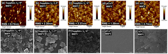
Figure 1.
Surface morphology of β-Ga2O3 films heteroepitaxially grown on various substrates at 800 °C: (a–e) AFM top-view images (5 × 5 μm2 scan areas), and (f–j) corresponding SEM images (scale bar: 500 nm).
This effect is corroborated by AFM (5 × 5 μm2 scan) and SEM images (with a 500 nm scale bar), which reveal the direct impact of substrate-film lattice mismatch on the macroscopic grain structure and surface morphology [19,20]. For instance, the film grown on c-plane sapphire without an off-cut angle exhibits significantly larger surface fluctuations. Its root mean square (RMS) roughness and the peak-to-valley height difference (as indicated in the AFM images) are approximately 4–5 times greater than those of films grown on other substrates under the same conditions. The underlying reason for this pronounced roughness will be discussed in a subsequent section.
The SEM images of films grown on sapphire substrates with different off-cut angles provide further insight. The film on the 6° off-cut sapphire demonstrates a relatively smooth surface with nearly continuous features. In contrast, films on 0° and 1.5° off-cut substrates display prominent, isolated protrusions. These features resemble monoclinic β-Ga2O3 aggregates with similar shapes and orientations, suggesting island-like growth. The superior morphology of the film on the 6° off-cut substrate implies that its surface provides more favorable atomic steps, conducive to the ideal growth of β-Ga2O3 [21].
Similarly, the film grown on the AlN template also exhibits a comparable, smooth morphology. Notably, the AFM and SEM results for the film on the pGaN template reveal the visually smoothest surface among all samples [22,23]. However, a comprehensive assessment of its crystalline quality requires further analysis in the following sections.
When the growth temperature is lowered to 400 °C, the situation changes markedly. Figure 2 presents the corresponding surface morphology of the films grown at 400 °C, as examined by AFM and SEM. The adsorbed molecules have substantially reduced migration energy due to the limited thermal budget. They tend to become immobilized before reaching the lowest-energy lattice sites, favoring a three-dimensional, island-like (Volmer-Weber) growth mode. Furthermore, the insufficient thermal energy may lead to incomplete decomposition of the metalorganic precursors and/or ineffective incorporation of oxygen species into the crystal lattice. As evidenced by both AFM and SEM, all five samples grown at this temperature exhibit a characteristic rough, porous morphology composed of fine, granular clusters [23].
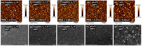
Figure 2.
Surface morphology of β-Ga2O3 films heteroepitaxially grown on various substrates at 400 °C: (a–e) AFM top-view images (5 × 5 μm2 scan areas), and (f–j) corresponding SEM images (scale bar: 500 nm).
Among these low-temperature samples, the film on the AlN template stands out as an exception, displaying a surface roughness approximately twice that of the others. This unique behavior warrants further investigation in subsequent characterizations.
Figure 3 presents the XRD ω-2θ scan patterns of the β-Ga2O3 films grown at 800 °C. The distinct diffraction peaks observed at 18.9°, 38.4°, and 59.1° are assigned to the (−201), (−402), and (−603) planes of β-Ga2O3, respectively. This series of well-defined peaks confirms the successful heteroepitaxial growth of single-crystal β-Ga2O3 films with excellent crystalline quality at this temperature. The peak located at 41.7° originates from the sapphire substrate. Additionally, the characteristic peaks of the underlying templates are detected at 34.6° for the pGaN substrate and at 35.9° for the AlN substrate, corresponding to the GaN (002) and AlN (002) reflections, respectively.
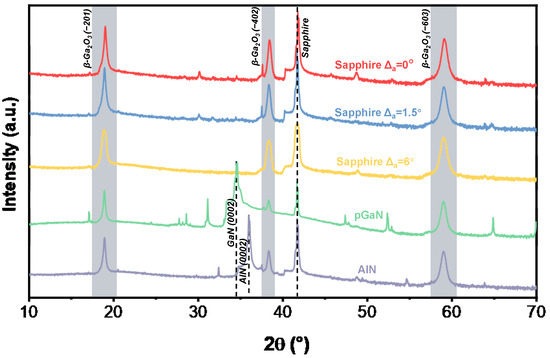
Figure 3.
XRD ω-2θ scans of β-Ga2O3 films grown on different substrates at 800 °C.
A notable finding is the appearance of multiple secondary peaks in the XRD pattern of pGaN substrate. These extraneous peaks are located at 17.0°, 27.7°, 28.6°, 47.4°, 52.3°, and 64.8° [24]. Comparative analysis with standard XRD databases reveals that their presence is primarily attributed to two interrelated factors:
Formation of Polycrystalline β-Ga2O3: The peaks at 27.7°, 47.4°, and 64.8° are identified as reflections from the (111), (020), and (800) planes of polycrystalline β-Ga2O3, respectively. Their emergence signifies the nucleation of randomly oriented β-Ga2O3 grains, which competes with the dominant (−201)-oriented epitaxial growth. This phenomenon is likely driven by the significant lattice mismatch and high interfacial energy between β-Ga2O3 and the p-GaN template.
Interfacial Reaction and Template Degradation: The peaks at 17.0° and 28.6° suggest complex interfacial reactions. The peak at 17.0° may be indexed to the (10−10) plane of GaN, potentially indicating texture evolution or strain relaxation within the underlying template. The peak at 28.6° does not match any common Ga2O3 polymorphs. Instead, it is hypothesized to originate from a gallium oxynitride (GaON) transition layer, formed due to the interdiffusion of oxygen and nitrogen atoms at the high-temperature growth interface.
In summary, the coexistence of the dominant (−201) epitaxial phase with polycrystalline β-Ga2O3 and interfacial reaction products underscores the substantial challenge in achieving phase-pure β-Ga2O3 epitaxy on p-GaN, stemming from inherent chemical and structural incompatibilities.
The crystal quality and stress state of the heteroepitaxial β-Ga2O3 films were systematically analyzed using XRD. Table 1 summarizes the peak positions of the (−201), (−402), and (−603) planes for films grown at 800 °C on different substrates. The deviation of these peaks from the standard β-Ga2O3 PDF card values (−201: 18.94°, −402: 38.38°, −603: 59.08°) is discussed [25], along with the determined type of stress (compressive or tensile) induced by each substrate. Furthermore, the full width at half maximum (FWHM), crystallite size, and dislocation density, which provide additional insights into the crystalline perfection, are presented in Figure 4.

Table 1.
XRD Peak Positions and Stress State Results for Gallium Oxide Heteroepitaxial Films at 800 °C.
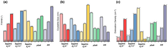
Figure 4.
Histograms of (a) FWHM, (b) crystallite size, and (c) dislocation density for different diffraction peaks of β-Ga2O3 films grown at 800 °C, derived from XRD measurements.
The Full Width at Half Maximum (FWHM) Calculation for each peak was determined by interpolating the XRD data around the peak and calculating the width at half maximum intensity. The FWHM values were used for subsequent crystallite size and dislocation density calculations.
The crystallite size (D) was estimated using the Scherrer equation [26]:
where is the Scherrer constant (shape factor), is the wavelength of Cu Kα radiation, is the FWHM in radians (converted from degrees), and is the Bragg angle in radians (half of the measured 2θ value).
The dislocation density (δ) was calculated using the following formula, which relates to the crystallite size [27]:
where D is the crystallite size in cm. This formula assumes that dislocations are uniformly distributed and that the crystallite size represents the average domain size free of dislocations.
These calculations provide quantitative insights into the film’s microstructure, including stress state, crystallite size, and defect density, which are critical for evaluating the quality of heteroepitaxial growth.
At the growth temperature of 800 °C, the β-Ga2O3 film grown on the sapphire substrate without an off-cut is the only sample that exhibits compressive stress across all measured crystal planes. This distinct stress state, which differs from that observed in other samples, is likely a primary contributor to its significantly larger surface fluctuations.
For the film on the 6° off-cut sapphire substrate, the full width at half maximum (FWHM) of the (−201), (−402), and (−603) diffraction peaks progressively decreases. This trend is opposite to that observed for the 0° and 1.5° off-cut substrates. This indicates that for the film on the 6° off-cut substrate, the (−201) plane possesses the smallest crystallite size, while the (−603) plane exhibits the lowest dislocation density compared to the other planes. This improved crystallinity with higher diffraction order suggests that the well-defined atomic steps provided by the 6° off-cut surface facilitate superior epitaxial growth, which is responsible for the exceptionally smooth morphology.
It is noteworthy that the FWHM from XRD ω-2θ scans shows an increasing trend with larger off-angle substrate, which is primarily attributed to the increased nucleation density and grain refinement on high-step-density surfaces. However, this does not equate to an overall degradation of crystal quality. Literature [28] reports that in similar systems, films grown on large off-angle substrates exhibit significantly reduced XRD rocking curve FWHM, indicating substantially improved orientation uniformity. This comparison reveals the dual role of off-angle substrate in heteroepitaxy: on one hand, it increases nucleation centers through high-density atomic steps, refining grain size; on the other hand, it forces grains to grow along specific orientations through these ordered steps, reducing mosaic spread. Therefore, the selection of off-angle substrate represents a crucial trade-off between controlling grain size and optimizing crystal orientation.
Regarding the film on the pGaN substrate, its remarkably smooth surface observed by both AFM and SEM can be attributed to the formation of polycrystalline phases. It is postulated that the random nucleation of polycrystalline grains effectively relieved the epitaxial strain. Consequently, a superior surface morphology was achieved at the expense of crystalline phase purity.
The crystallinity of the ε-Ga2O3 films was critically dependent on the underlying template. X-ray diffraction (XRD) 2θ-ω scans were employed to assess the phase purity, as shown in Figure 5.
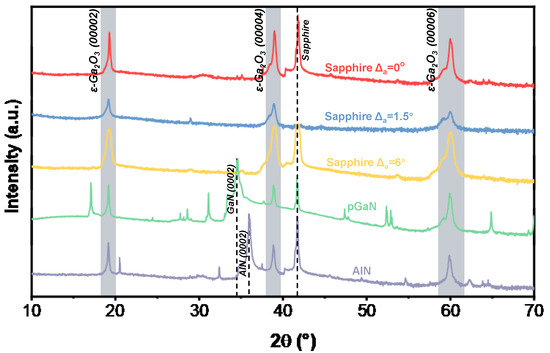
Figure 5.
XRD ω-2θ scans of ε-Ga2O3 films grown on different substrates at 400 °C.
During the growth process at 400 °C, ε-phase gallium oxide was obtained, with its (0002), (0004), and (0006) diffraction peaks located at 19.3°, 39.0°, and 60.0°, respectively. Notably, the (0006) diffraction peak is not symmetric; a shoulder peak approximately at 59.1° is consistently observed on the left side in each sample, indicating the simultaneous presence of β-Ga2O3.
When ε-Ga2O3 was heteroepitaxially grown on a p-GaN/Al2O3 template, the diffraction pattern revealed multiple secondary peaks at 17.07°, 31°, 52.3°, 52.87°, and 64.87°. These peaks are identified as polycrystalline β-Ga2O3, which is the thermodynamically stable phase. The formation of the β-phase is attributed to the significant lattice mismatch and the instability of the GaN surface under oxidizing growth conditions, which promotes random nucleation of the stable polymorph.
In contrast, growth on an AlN/Al2O3 template yielded a significant improvement in phase purity. The dominant peaks correspond to the ε-Ga2O3 phase. However, minor secondary peaks were observed at 20.49° and 32.4°, which are associated with α-Ga2O3. The emergence of these defects is likely due to non-optimal growth kinetics, as the hexagonal AlN template provides a superior structural match for the metastable ε-phase. This result confirms that AlN is a more suitable template for the heteroepitaxy of pure ε-Ga2O3, though further process optimization is required to completely suppress competing phases.
A systematic analysis of the crystal quality and stress state for the films grown at 400 °C was conducted via XRD. The peak positions for the (0002), (0004), and (0006) planes, corresponding to the ε-Ga2O3 phase, are detailed in Table 2 for each substrate. The observed shifts in these peaks from the reference values of the ε-Ga2O3 PDF card (0002: 19.20°, 0004: 38.60°, 0006: 59.40°) are evaluated and attributed to the strain induced by the substrate [29], with the nature of the stress (compressive or tensile) specified. Complementary parameters, including the FWHM, crystallite size, and dislocation density derived from these measurements, are provided in Figure 6.
Table 2.
XRD Peak Positions and Stress State Results for Gallium Oxide Heteroepitaxial Films at 400 °C.
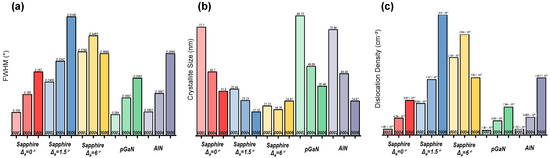
Figure 6.
Histograms of (a) FWHM, (b) crystallite size, and (c) dislocation density for different diffraction peaks of ε-Ga2O3 films grown at 400 °C, derived from XRD measurements.
The XRD peak positions for the 0° and 6° off-cut sapphire substrates consistently shift to higher angles across all measured planes, indicating the presence of compressive stress within the films, which leads to a reduction in interplanar spacing.
In contrast, the films on the 1.5° off-cut sapphire, pGaN, and AlN substrates exhibit a more complex stress state. The (0002) plane shows signs of tensile stress, while the (0004) and (0006) planes indicate compressive stress. This non-uniform stress distribution reveals significant stress anisotropy, likely originating from lattice mismatch or defect formation during heteroepitaxy. For these samples, the crystallite size decreases, and the dislocation density increases with higher-order reflections. This trend suggests that the higher-index planes are more sensitive to microstructural defects. The concomitant increase in FWHM further confirms a gradual degradation of crystalline quality along the c-axis direction. The observed peak shifts from the standard ε-Ga2O3 positions are attributed to substrate-induced strain and specific growth conditions.
Specifically for the 0°, 1.5° sapphire, pGaN, and AlN substrates, the (0002) plane exhibits the smallest FWHM, the largest crystallite size, and the lowest dislocation density, indicating the highest crystalline perfection near this orientation. The degradation in FWHM, crystallite size, and dislocation density for the (0004) and (0006) planes confirms that crystal quality deteriorates progressively along the c-axis. In summary, while the film growth is preferential along the [0002] direction, significant stress inhomogeneity persists, necessitating further optimization of growth parameters to mitigate stress and reduce dislocation densities.
The calculated crystallite sizes at 400 °C do not show a marked difference from those at 800 °C. This implies that the distinct grain morphologies observed by SEM at these two temperatures are primarily due to differences in the macroscopic aggregation of grains, rather than a fundamental change in the primary crystallite size. This aggregation state is governed by the surface migration energy of adatoms, which is substantially lower at 400 °C. The restricted atomic mobility at the lower temperature results in a “lazier” adatom behavior, inhibiting the reorganization into thermodynamically stable configurations. Conversely, at 800 °C, where migration energy is sufficient, heteroepitaxial β-Ga2O3 growth is driven to find low-energy sites, which, due to lattice and thermal mismatch with the substrates, paradoxically results in macroscopically rougher surface morphologies.
Furthermore, the notably larger surface roughness observed for the AlN substrate at 400 °C via AFM and SEM could be attributed to the coexistence of multiple Ga2O3 polymorphs (β, ε, and α phases), introducing additional phase boundaries and mismatch, thereby exacerbating the surface instability.
In general, XRD results indicate that the films on sapphire without an off-cut and on pGaN substrates exhibit relatively narrower FWHM at both 400 °C and 800 °C compared to other substrates. However, the pGaN substrate also presents numerous secondary phases, implying poorer crystalline phase purity. This observation reveals an important discrepancy when correlated with AFM and SEM findings: a smoother surface morphology does not necessarily equate to higher crystalline quality or phase purity. This underscores the necessity for complementary characterization techniques to obtain a comprehensive understanding of the film properties. Further in-depth analysis is required to elucidate the underlying mechanisms.
Figure 7 summarizes the calculated lattice and thermal mismatch for the gallium oxide films grown on various substrates at different temperatures [30].
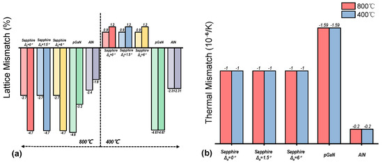
Figure 7.
Histograms illustrating the (a) lattice mismatch and (b) thermal mismatch between the heteroepitaxial gallium oxide films and various substrates.
The lattice mismatch for β-Ga2O3 and ε-Ga2O3 on sapphire substrates was calculated based on common epitaxial relationships, such as β-Ga2O3(−201) || Al2O3(0001). For β-Ga2O3 on pGaN(0002) and AlN(0002), the calculation was based on relationships like β-Ga2O3(−201) || GaN(0001). Since ε-Ga2O3 possesses a hexagonal structure and exhibits in-plane isotropy, only one lattice mismatch value (along the [11,12,13,14,15,16,17,18,19,20] direction) is listed for it.
The thermal mismatch was derived from the difference in the in-plane coefficients of thermal expansion (CTE) between the substrates and the gallium oxide films. The employed CTE values were approximately 5.0 × 10⁻⁶/K for sapphire, 4.0 × 10⁻⁶/K for both β-Ga2O3 and ε-Ga2O3, 5.59 × 10⁻⁶/K for GaN, and 4.2 × 10⁻⁶/K for AlN. It is noted that the actual mismatch may vary slightly depending on specific growth conditions and film thickness.
Notably, the pGaN substrate exhibits the largest lattice and thermal mismatch with gallium oxide among all substrates at both 800 °C and 400 °C. However, its XRD results show the narrowest FWHM alongside the highest number of secondary phases. In contrast, the AlN substrate demonstrates a relatively smaller thermal mismatch at both temperatures.
The survey XPS spectra of the films grown on different substrates at 800 °C and 400 °C are presented in Figure 8. Distinct peaks corresponding to gallium (Ga) and oxygen (O) confirm the formation of gallium oxide films. Subsequent high-resolution analysis of the O 1s peak was performed, with the spectra deconvoluted into at least two components: a low-binding-energy component (~530.0–530.6 eV), attributed to the Ga–O bonds (lattice oxygen) in β-Ga2O3, and a high-binding-energy component (~531.2–532.0 eV), ascribed to surface species such as hydroxyl groups (-OH), adsorbed water (H2O), or carbonates [31]. The percentage of lattice oxygen and the ratio of adsorbed oxygen to lattice oxygen were extracted from this analysis and are displayed in this study.
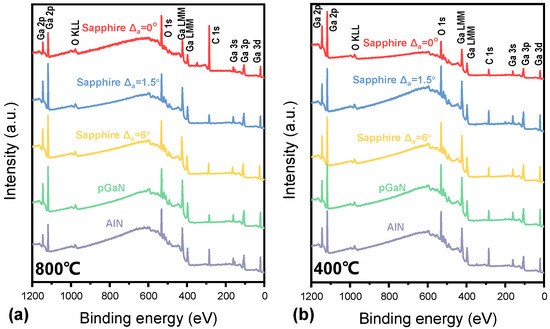
Figure 8.
XPS survey spectra (0–1200 eV) of gallium oxide films grown under ten different conditions (combining two temperatures and five substrates): (a) 800 °C and (b) 400 °C.
Figure 9 summarizes the quantitative results, showing the lattice oxygen percentage and the adsorbed-oxygen-to-lattice-oxygen ratio. For the film grown at 800 °C on the sapphire substrate without an off-cut, the O 1s spectrum exhibits a lower lattice oxygen percentage and a higher adsorbed-oxygen-to-lattice-oxygen ratio. This indicates a higher density of surface defects, which is consistent with its inferior surface morphology observed by AFM/SEM. Meanwhile, samples grown at 400 °C generally show a higher proportion of adsorbed oxygen. The significantly higher proportion of adsorbed oxygen species in the XPS O 1s spectra of the 400 °C samples indicates a higher density of surface sites with high reactivity.
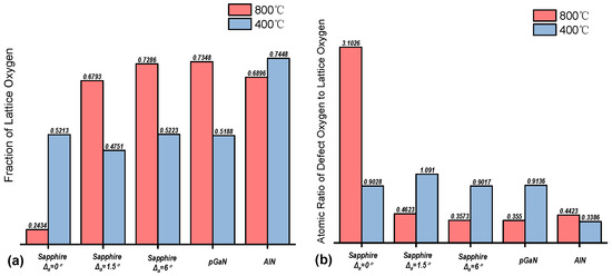
Figure 9.
Histograms of the relative percentages of (a) the fraction of lattice oxygen and (b) the atomic ratio of defective oxygen to lattice oxygen in the O 1s region for films grown under 800 °C and 400 °C, obtained from peak deconvolution of high-resolution XPS spectra.
The energy-dispersive X-ray (EDX) spectroscopy mapping (10 kV accelerating voltage) results are presented in Figure 10, which provides the elemental composition and spatial distribution of Ga and O. A quantitative analysis of the O/Ga atomic ratio was performed, and the results are compared with those from XPS.
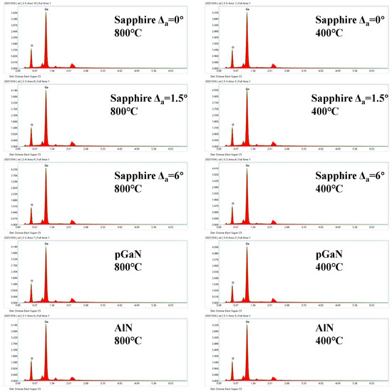
Figure 10.
Elemental mapping results from energy-dispersive X-ray (EDX) spectroscopy for gallium oxide films grown under ten different conditions (combining two temperatures and five substrates).
Figure 11 displays a statistical graph of the O/Ga atomic ratio for all samples, offering an intuitive visualization of the oxygen deficiency and its correlation with both growth temperature and substrate type. The films grown at 800 °C exhibit a higher O/Ga atomic ratio compared to those grown at 400 °C, indicating a composition closer to the ideal stoichiometric value of 3:2 and thus higher quality gallium oxide films [21]. Among the different substrates at 800 °C, the AlN substrate yields the best result (closest to stoichiometry), while the pGaN substrate gives the poorest. This trend aligns with the lattice and thermal mismatch data presented earlier: pGaN has the largest mismatch with Ga2O3, while AlN has a relatively smaller mismatch. For the sapphire substrates, the film on the 6° off-cut substrate shows a superior O/Ga ratio at 800 °C, whereas the 1.5° off-cut substrate is more favorable at 400 °C.
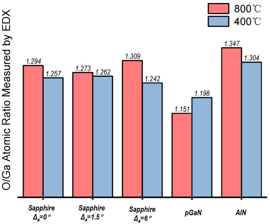
Figure 11.
Histogram of O/Ga atomic ratios derived from EDX analysis for gallium oxide films grown under ten different conditions.
In summary, the samples grown at 800 °C are more stoichiometric than those grown at 400 °C, implying more sufficient incorporation and reaction between Ga and O precursors at the elevated temperature. Furthermore, the oxygen incorporation efficiency varies significantly across different substrates. The superior performance of the AlN substrate can be linked to its high chemical stability. In contrast, the poor result for the pGaN substrate may be attributed to its pronounced lattice/thermal mismatch and the potential thermal decomposition of the underlying GaN template, which could detrimentally affect oxygen incorporation during growth.
Figure 12 presents Raman spectra of β-Ga2O3 heteroepitaxial films grown at 800 °C and 400 °C on various substrates. The characteristic phonon modes for both the epitaxial β-Ga2O3 films and the underlying substrates are identified and labeled in the figure. The observed peak positions and their assignments are summarized in Table 3. The data conclusively confirm the successful heteroepitaxial growth of β-Ga2O3, as evidenced by the presence of its characteristic Ag and Bg modes [32]. The detection of substrate-related peaks (from sapphire, GaN, and AlN) confirms the sufficient penetration depth of the 532 nm laser excitation source.
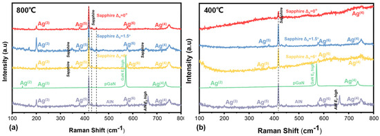
Figure 12.
Raman spectra of gallium oxide films grown under ten different conditions: (a) 800 °C and (b) 400 °C.
Table 3.
Raman Peak Position Results for Gallium Oxide Heteroepitaxial Films.
At the growth temperature of 800 °C, the characteristic Raman peak is consistently observed at 200.57 cm−1 for films on all five substrates. This uniformity in peak position indicates an effective release of intrinsic stress within the epitaxial films. The corresponding full width at half maximum (FWHM) values for the five substrates are 2.5, 2.53, 3.49, 2.3, and 2.33 cm−1, respectively.
In contrast, at the lower temperature of 400 °C, the Ag(3) phonon mode is only detectable in the film grown on the AlN substrate. The absence of this characteristic peak in other samples can be primarily attributed to their poorer overall crystalline quality. Furthermore, the Raman spectrum acquired from the AlN sample exhibits a distinctive hump-shaped background. This feature is likely associated with fluorescence effects occurring at the film surface, which can interfere with the Raman signal.
4. Conclusions
In summary, this study identifies 800 °C as the optimal growth temperature for high-quality β-Ga2O3 heteroepitaxy, yielding superior crystallinity, improved stoichiometry (closer to the ideal O/Ga ratio of 3:2), and a reduced oxygen deficiency. The 6° off-cut sapphire and AlN/sapphire substrates are the most favorable, effectively mitigating non-stoichiometry and defect formation. A key finding is that surface smoothness can be misleading, as it does not guarantee high phase purity or controlled oxygen deficiency, exemplified by the p-GaN substrate. These results provide clear guidelines for optimizing chemical composition and defect control in β-Ga2O3 device fabrication.
Author Contributions
Conceptualization, Y.L.; Methodology, Y.Z., S.X. and J.M.; Software, K.W.; Validation, S.X. and J.M.; Formal analysis, Y.L. and K.W.; Investigation, Y.L., G.P. and Y.Y.; Resources, Y.Z., S.X., Y.H. and J.Z.; Data curation, Y.L. and Y.Y.; Writing—original draft, Y.L.; Writing—review & editing, Y.Z.; Visualization, Y.L. and K.W.; Supervision, Y.Z., Y.H. and J.Z.; Project administration, Q.F. and J.Z.; Funding acquisition, Y.Z., Y.H. and J.Z. All authors have read and agreed to the published version of the manuscript.
Funding
This research was funded by National Natural Science Foundation of China (Grant No. 62174127), National Key Research and Development Program (Grant No. 2021YFB3601102), Key Research and Development Program of Jiangsu Province (Grant No. BE2020004-4), Shanxi Province Key Research and Development Program (Grant No. 202202030201001). We would also like to thank the Hefei Comprehensive National Science Center and Jiangsu Institute of Advanced Semiconductors Co. Ltd. And The APC was funded by Xidian University.
Data Availability Statement
The original contributions presented in this study are included in the article. Further inquiries can be directed to the corresponding author(s).
Conflicts of Interest
The authors declare no conflict of interest.
References
- Higashiwaki, M. β-Ga2O3 material properties, growth technologies, and devices: A review. AAPPS Bull. 2022, 32, 3. [Google Scholar] [CrossRef]
- Green, A.J.; Speck, J.; Xing, G.; Moens, P.; Allerstam, F.; Gumaelius, K.; Neyer, T.; Arias-Purdue, A.; Mehrotra, V.; Kuramata, A.; et al. β-Gallium oxide power electronics. APL Mater. 2022, 10, 029201. [Google Scholar] [CrossRef]
- Alema, F.; Zhang, Y.; Osinsky, A.; Valente, N.; Mauze, A.; Itoh, T.; Speck, J.S. Low temperature electron mobility exceeding 104 cm2/V s in MOCVD grown β-Ga2O3. APL Mater. 2019, 7, 121110. [Google Scholar] [CrossRef]
- Waseem, A.; Ren, Z.; Huang, H.-C.; Nguyen, K.; Wu, X.; Li, X. A Review of Recent Progress in β-Ga2O3 Epitaxial Growth: Effect of Substrate Orientation and Precursors in Metal–Organic Chemical Vapor Deposition. Phys. Status Solidi A 2022, 220, 2200616. [Google Scholar] [CrossRef]
- Feng, Z.; Bhuiyan, A.F.M.A.U.; Karim, M.R.; Zhao, H. MOCVD homoepitaxy of Si-doped (010) β-Ga2O3 thin films with superior transport properties. Appl. Phys. Lett. 2019, 114, 250601. [Google Scholar] [CrossRef]
- Xie, L.; Zhang, T.; Xu, S.; Su, H.; Tao, H.; Gao, Y.; Liu, X.; Zhang, J.; Hao, Y. The Barrier Inhomogeneity and the Electrical Characteristics of W/Au β-Ga2O3 Schottky Barrier Diodes. Micromachines 2025, 16, 369. [Google Scholar] [CrossRef] [PubMed]
- Yoon, S.; Oh, S.; Lee, G.; Kim, Y.; Kim, S.; Park, J.-H.; Shin, M.; Jeon, D.-W.; Yoo, G. Enhanced UVC Responsivity of Heteroepitaxial α-Ga2O3 Photodetector with Ultra-Thin HfO2 Interlayer. Micromachines 2025, 16, 836. [Google Scholar] [CrossRef] [PubMed]
- Pratiyush, A.S.; Krishnamoorthy, S.; Solanke, S.V.; Xia, Z.; Muralidharan, R.; Rajan, S.; Nath, D.N. High responsivity in molecular beam epitaxy grown β-Ga2O3 metal semiconductor metal solar blind deep-UV photodetector. Appl. Phys. Lett. 2017, 110, 221107. [Google Scholar] [CrossRef]
- Yao, Y.; Gangireddy, R.; Kim, J. Electrical behavior of β-Ga2O3 Schottky diodes with different Schottky metals. J. Vac. Sci. Technol. B 2017, 35, 03D113. [Google Scholar] [CrossRef]
- Farzana, E.; Alema, F.; Ho, W.Y.; Mauze, A.; Itoh, T.; Osinsky, A.; Speck, J.S. Vertical β-Ga2O3 field plate Schottky barrier diode from metal-organic chemical vapor deposition. Appl. Phys. Lett. 2021, 118, 162109. [Google Scholar] [CrossRef]
- Mochalov, L.A.; Telegin, S.V.; Almaev, A.V.; Slapovskaya, E.A.; Yunin, P.A. Structural and Electrically Conductive Properties of Plasma Enhanced Chemical-Vapor-Deposited High-Resistivity Zn-Doped β-Ga2O3 Thin Films. Micromachines 2025, 16, 954. [Google Scholar] [CrossRef]
- Zhang, C.; Liu, K.; Ai, Q.; Sun, X.; Chen, X.; Yang, J.; Zhu, Y.; Cheng, Z.; Li, B.; Liu, L.; et al. High-performance fully transparent Ga2O3 solar-blind UV photodetector with the embedded indium–tin–oxide electrodes. Mater. Today Phys. 2023, 33, 101034. [Google Scholar] [CrossRef]
- Lu, C.-H.; Tarntair, F.-G.; Kao, Y.-C.; Tumilty, N.; Shieh, J.-M.; Hsu, S.-H.; Hsiao, C.-L.; Horng, R.-H. β-Ga2O3 MOSFETs electrical characteristic study of various etching depths grown on sapphire substrate by MOCVD. Discov. Nano 2023, 18, 92. [Google Scholar] [CrossRef]
- Dimitrocenko, L.; Strikis, G.; Polyakov, B.; Bikse, L.; Oras, S.; Butanovs, E. The Effect of a Nucleation Layer on Morphology and Grain Size in MOCVD-Grown β-Ga2O3 Thin Films on C-Plane Sapphire. Materials 2022, 15, 8362. [Google Scholar] [CrossRef]
- Hsu, Y.-H.; Wu, W.-Y.; Lin, K.-L.; Chen, Y.-H.; Lin, Y.-H.; Liu, P.-L.; Hsiao, C.-L.; Horng, R.-H. ε-Ga2O3 Grown on c-Plane Sapphire by MOCVD with a Multistep Growth Process. Cryst. Growth Des. 2022, 22, 1837–1845. [Google Scholar] [CrossRef]
- Hajnal, Z.; Miró, J.; Kiss, G.; Réti, F.; Deák, P.; Herndon, R.C.; Kuperberg, J.M. Role of oxygen vacancy defect states in the n-type conduction of β-Ga2O3. J. Appl. Phys. 1999, 86, 3792. [Google Scholar] [CrossRef]
- McCluskey, M.D. Point defects in Ga2O3. J. Appl. Phys. 2020, 127, 101101. [Google Scholar] [CrossRef]
- Ghadi, H.; McGlone, J.F.; Feng, Z.; Bhuiyan, A.F.M.A.U.; Zhao, H.; Arehart, A.R.; Ringel, S.A. Influence of growth temperature on defect states throughout the bandgap of MOCVD grown β-Ga2O3. Appl. Phys. Lett. 2020, 117, 172106. [Google Scholar] [CrossRef]
- Joshi, G.; Chauhan, Y.S.; Verma, A. Temperature dependence of β-Ga2O3 heteroepitaxy on c-plane sapphire using low pressure chemical vapor deposition. J. Alloys Compd. 2021, 883, 160799. [Google Scholar] [CrossRef]
- Fan, M.-M.; Lu, Y.-J.; Xu, K.-L.; Cui, Y.-X.; Cao, L.; Li, X.-Y. Growth and characterization of Sn-doped β-Ga2O3 thin films by chemical vapor deposition using solid powder precursors toward solar-blind ultraviolet photodetection. Appl. Surf. Sci. 2020, 509, 144867. [Google Scholar] [CrossRef]
- Rafique, S.; Han, L.; Zhao, H. Synthesis of wide bandgap Ga2O3 (Eg∼4.6–4.7 eV) thin films on sapphire by low pressure chemical vapor deposition. Phys. Status Solidi A 2016, 213, 1002–1009. [Google Scholar] [CrossRef]
- Zhang, Y.; Li, Y.; Wang, Z.; Guo, R.; Xu, S.; Liu, C.; Zhao, S.; Zhang, J.; Hao, Y. Investigation of β-Ga2O3 films and β-Ga2O3/GaN heterostructures grown by metal organic chemical vapor deposition. Sci. China Phys. Mech. Astron. 2020, 63, 117311. [Google Scholar] [CrossRef]
- Li, Y.; Zhang, Y.; Zhang, J.; Zhang, T.; Xu, S.; Feng, L.; Feng, Q.; Zhang, C.; Hao, Y. Investigation on high quality ultra-wide band gap β-Ga2O3/AlN heterostructure grown by metal organic chemical vapor deposition. Semicond. Sci. Technol. 2022, 37, 095004. [Google Scholar] [CrossRef]
- Nakagomi, S.; Kokubun, Y. Crystal orientations of β-Ga2O3 thin films formed on c-plane GaN substrate. Phys. Status Solidi B 2016, 253, 1217–1221. [Google Scholar] [CrossRef]
- Leedy, K.D.; Chabak, K.D.; Vasilyev, V.; Look, D.C.; Boeckl, J.J.; Brown, J.L.; Tetlak, S.E.; Green, A.J.; Moser, N.A.; Crespo, A.; et al. Highly conductive homoepitaxial Si-doped Ga2O3 films on (010) β−Ga2O3 by pulsed laser deposition. Appl. Phys. Lett. 2017, 111, 012103. [Google Scholar] [CrossRef]
- Scherrer, P. Bestimmung der Größe und der inneren Struktur von Kolloidteilchen mittels Röntgenstrahlen. Nachrichten Ges. Wiss. Göttingen Math.-Phys. Kl. 1918, 26, 98–100. [Google Scholar]
- Williamson, G.K.; Smallman, R.E. III. Dislocation densities in some annealed and cold-worked metals from measurements on the X-ray debye-scherrer spectrum. Philos. Mag. 1956, 1, 34–46. [Google Scholar] [CrossRef]
- Rafique, S.; Han, L.; Neal, A.T.; Mou, S.; Boeckl, J.; Zhao, H. Towards High-Mobility Heteroepitaxial β-Ga2O3 on Sapphire: Dependence on the Substrate Off-Axis Angle. Phys. Status Solidi A 2018, 215, 1700467. [Google Scholar] [CrossRef]
- Zhang, T.; Li, Y.; Cheng, Q.; Hu, Z.; Ma, J.; Yao, Y.; Cui, C.; Zuo, Y.; Feng, Q.; Zhang, Y.; et al. Research on the crystal phase and orientation of Ga2O3 Hetero-epitaxial film. Superlattices Microstruct. 2021, 159, 107053. [Google Scholar] [CrossRef]
- Pearton, S.J.; Yang, J.; Cary, P.H., IV; Ren, F.; Kim, J.; Tadjer, M.J.; Mastro, M.A. A review of Ga2O3 materials, processing, and devices. Appl. Phys. Rev. 2018, 5, 011301. [Google Scholar] [CrossRef]
- Ma, Y.J.; Zhang, X.D.; Feng, B.Y.; Tang, W.B.; Chen, T.W.; Qian, H.; Zhang, L.; Zhou, X.; Wei, X.; Xu, K.; et al. Mis-cut direction of substrate effect on the photoresponse characteristic of β-Ga2O3 film. Vacuum 2022, 198, 110886. [Google Scholar] [CrossRef]
- Xie, L.; Xu, S.; Zhang, T.; Tao, H.; Su, H.; Gao, Y.; Liu, X.; Zhang, Y.; Zhang, J.; Hao, Y. Improved crystal quality of β-Ga2O3 films and performance enhancement of W/Au Schottky barrier diodes via in-situ two-step annealing. J. Alloys Compd. 2025, 1016, 178924. [Google Scholar] [CrossRef]
Disclaimer/Publisher’s Note: The statements, opinions and data contained in all publications are solely those of the individual author(s) and contributor(s) and not of MDPI and/or the editor(s). MDPI and/or the editor(s) disclaim responsibility for any injury to people or property resulting from any ideas, methods, instructions or products referred to in the content. |
© 2025 by the authors. Licensee MDPI, Basel, Switzerland. This article is an open access article distributed under the terms and conditions of the Creative Commons Attribution (CC BY) license (https://creativecommons.org/licenses/by/4.0/).