Article

Design of Dual Continuous-Mode Class-J Power Amplifiers with Harmonic Matching Networks for X and Ku Bands

by
Yang Yuan
1,
Xuesong Zhao
1,
Jingxin Fan
1,2 and
Zhongjun Yu
1,2,*
1
Aerospace Information Research Institute, Chinese Academy of Sciences, Beijing 100190, China
2
School of Electronic, Electrical and Communication Engineering, University of Chinese Academy of Sciences, Beijing 101408, China
*
Author to whom correspondence should be addressed.
Micromachines 2025, 16(12), 1362; https://doi.org/10.3390/mi16121362
Submission received: 8 November 2025 / Revised: 24 November 2025 / Accepted: 27 November 2025 / Published: 29 November 2025

Abstract

In this article, two wideband high-efficiency Class-J power amplifiers operating in X and Ku bands, respectively, are designed based on continuous mode. The optimal impedance regions of the transistors are determined using harmonic load-pull techniques. An on-chip output matching network with second harmonic control functionality is designed to achieve Class-J operation. To verify the feasibility of designed circuits, both power amplifiers are designed and fabricated using a 0.25 mm GaAs pseudomorphic high electron mobility transistor (pHEMT) process. The power amplifiers are both biased at 6 V/−1 V. The measured results show the X-band and Ku-band power amplifiers achieve peak saturated output powers of 31.2 dBm and 30.8 dBm, respectively. The power-added efficiencies (PAEs) of the two amplifiers within their operating bands reach up to 48% and 45.3%, respectively. Compact size and high efficiency make them suitable for integration into phased array transmit/receiver (T/R) modules.

1. Introduction

Modern active phased arrays demand multifunctionality and lightweight design [1]. Accordingly, the widebanding and miniaturization of transmit/receiver (T/R) modules become imperative. Among these requirements, thermal design is a core factor restricting the miniaturization of T/R modules, while the efficiency of T/R modules is primarily determined by their internal power amplifiers [2]. However, the widebanding of power amplifiers leads to efficiency degradation. Therefore, designing wideband high-efficiency power amplifiers is key to realizing the multifunctionality and lightweight design of phased arrays.
Based on waveform engineering analysis, continuous-mode power amplifiers maintain high efficiency over a wide bandwidth, making them ideal for designing saturated power amplifiers in T/R modules [3]. A waveform-engineered sequential load-modulated balanced amplifier, which employs continuous Class-F−1 and Class-J operations, achieves a saturated drain efficiency of 60.2–68.3% across 1.80–2.75 GHz [4]. An ultrawideband power amplifier utilizing a novel multi-branch matching network and extended continuous Class-B/J modes delivers a drain efficiency of 56–70% over 0.4–3.8 GHz, with a relative bandwidth of 162% [5]. The power amplifiers reported in [4,5] employ off-chip high-Q output matching networks (OMNs), achieving high efficiency over a wide bandwidth. However, their large overall footprint renders them incompatible with the integration into transmit/receive (T/R) modules. In [6], an X-band Class-J power amplifier based on active load modulation is implemented in a 0.25 mm GaAs pseudomorphic high electron mobility transistor (pHEMT) process, achieving a peak power-added efficiency (PAE) of 50% over 9.1~10.8 GHz with a die area of 1.89 × 1.69 mm2. Ref. [7] demonstrates a broadband power amplifier fabricated in a 0.25 μm GaN HEMT process, realizing a PAE of 36.3–47% across 2–6 GHz.
In this article, two wideband high-efficiency Class-J power amplifiers operating in the X band and Ku band, respectively, are designed and fabricated using a 0.25 mm GaAs pHEMT process. On-chip second harmonic control network is integrated into the OMN to realize the Class-J operation. The measured results show that both power amplifiers exhibit high PAE within their respective bandwidths. Furthermore, their compact footprint renders them suitable for integration with miniaturized T/R modules.

2. Continuous-Mode Class-J Power Amplifier

Continuous-mode power amplifiers expand the solution space for the optimal load impedance, thereby enhancing the design flexibility of the output matching network and allowing the power amplifier to maintain high drain efficiency over a broad frequency band [8].
Taking the continuous Class-J power amplifier as an example, the drain-source current id_J and voltage vd_J of the transistor can be given by Equations (1) and (2), respectively [9].
i d _ J = I m π + I m 2 cos θ + 2 I m 3 π cos 2 θ 2 I m 15 π cos 4 θ +
v d _ J = V D 1 cos θ 1 α sin θ             = V D 1 α 2 + 1 sin θ + arctan 1 α + α 2 sin 2 θ
Here, α [ 1 ,   1 ] , Im and VD are the peak current and the bias voltage, respectively. The power amplifier operates in Class-J mode for all values of a, with the exception of a = 0 (Class-B). Based on Equations (1) and (2), the impedance conditions for continuous Class-J power amplifiers are
Z n _ J = 2 V D I m 1 + j α ,   n = 1 j 3 π V D 4 I m α ,   n = 2 0 ,   n > 2
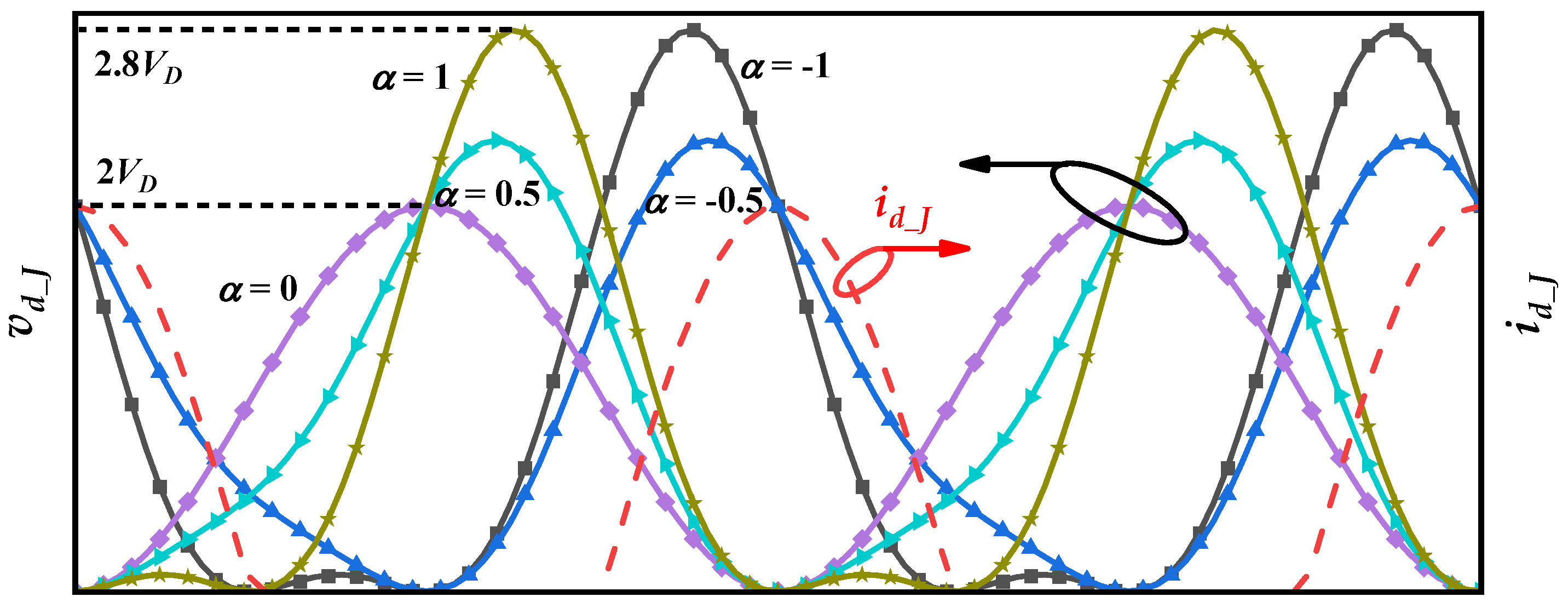
where n is the harmonic order. Equation (3) demonstrates that different values of a produce distinct impedance traces on the Smith chart, as shown in Figure 1, which facilitates broadband matching of the amplifier. Furthermore, as the additional impedance introduced at the second-harmonic frequency is purely reactive, it theoretically imposes no degradation on the amplifier efficiency. Figure 2 shows the waveforms of vd_J and id_J for different values of a. For the Class-J amplifiers, it can be observed that affected by the second harmonic, the waveform of vd_J shifts left or right under different values of a (relative to a = 0) [10].

3. Harmonic Load Pull

To achieve the design of a continuous-mode broadband high-efficiency power amplifier, in addition to performing fundamental load pull, it is also necessary to determine the range of the second harmonic impedance. The selected transistor based on a 0.25 mm GaAs pHEMT process features a maximum drain-source voltage of 18 V. As can be seen from Figure 2, in continuous-mode operation, the peak voltage of vds exceeds the drain bias voltage VD by approximately 2.8 times. To avoid transistor breakdown caused by excessive peak voltage, VD is ultimately set to 6 V.
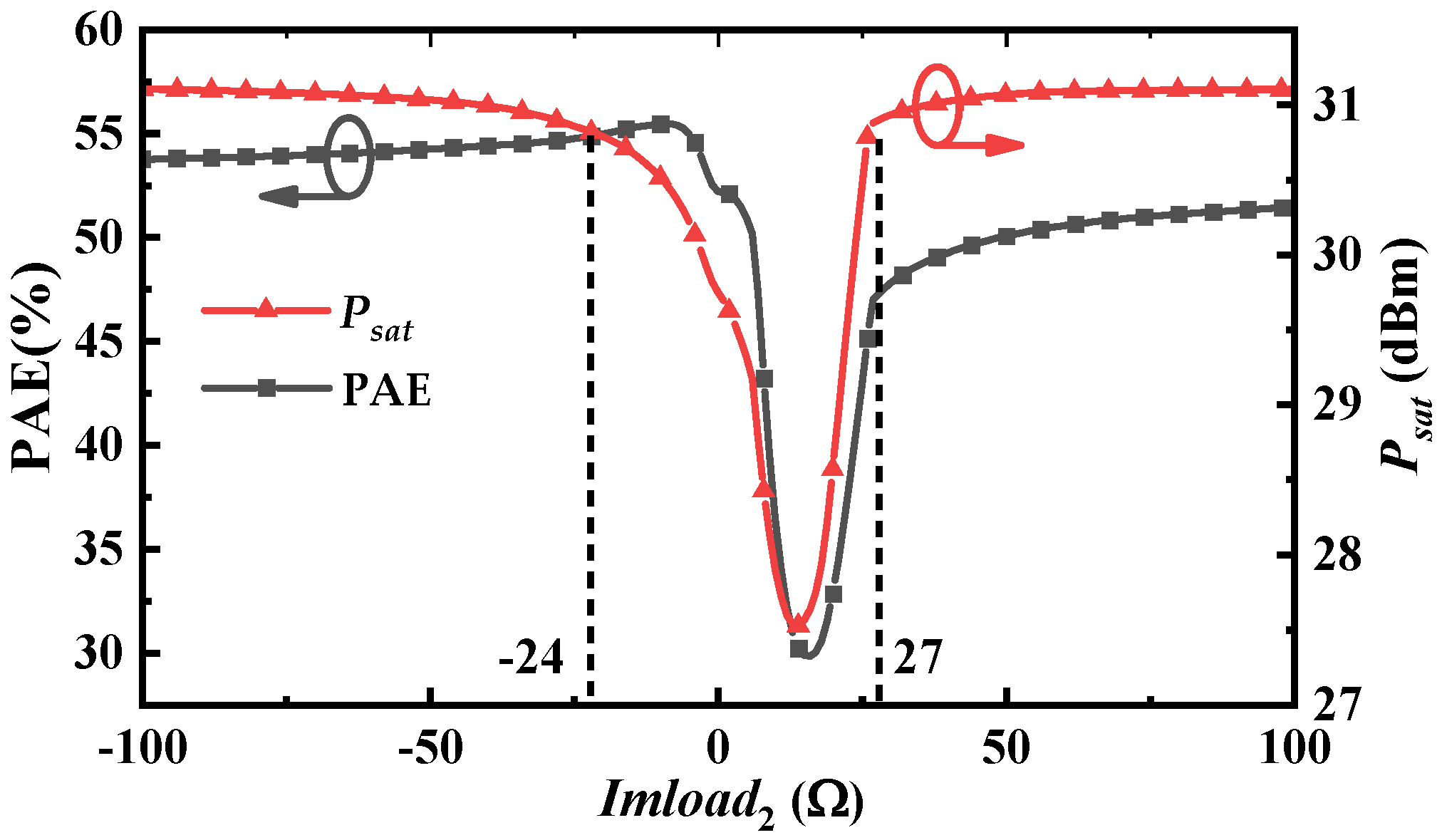
Under a 6 V/−1 V bias condition, fundamental load pull is conducted on the output-stage transistors of the X-band and Ku-band power amplifiers. The resulting optimum impedances serve as the initial values for subsequent iterations. To simulate practical losses, the real part of the second harmonic impedance is fixed at 5 W, while a parameter sweep is performed over its imaginary part (Imload2). Figure 3 plots the saturated output power (Psat) and PAE of the X-band transistor versus Imload2. The results reveal a sharp degradation in both Psat and PAE within the Imload2 range of −j24 W to j27 W.
Based on the second harmonic parameter sweep, appropriate harmonic load values are selected. After multiple iterations of fundamental load-pull and harmonic impedance sweeps, the final fundamental and harmonic impedance values are obtained. Table 1 presents the results of source pull and harmonic load pull for the output-stage transistors of the X-band and Ku-band power amplifiers.

4. Design of the Harmonic Matching Network

As shown in Figure 1 and Table 1, the second harmonic load is purely reactive. Consequently, the output matching network must achieve a dual function: transforming the 50 Ω source impedance to the fundamental impedance Zf0, while concurrently providing the required harmonic impedance Z2f0. Although the off-chip branch-line structure can readily implement such harmonic matching, its large circuit area makes it unsuitable for integration in phased array T/R modules [11]. Fortunately, advances in semiconductor technology now permit the on-chip integration of harmonic control networks. While this approach may incur a slight efficiency penalty compared to off-chip, high-Q matching circuits, the significantly reduced amplifier area facilitates integration within T/R modules. Figure 4 shows the schematic diagram of the designed impedance matching network with a second harmonic control function.
In Figure 4, Lp and Cp resonate at 2f0 to realize second harmonic short-circuiting, whereas at the fundamental frequency, they are equivalent to a shunt grounded capacitor Ceq. Equation (4) presents the relationship between Cp and Ceq. Ls is employed to tune Imload2 to meet the requirements of Z2f0 specified in Table 1. L1, C1, C2, Ceq, and Ls form a fifth-order matching network, achieving fundamental impedance matching for both the X and Ku bands. The drain bias inductor Ld1 is placed before the series resonant network; to avoid affecting the second harmonic, it has a large inductance value and does not participate in impedance matching.
C p = 3 4 C e q
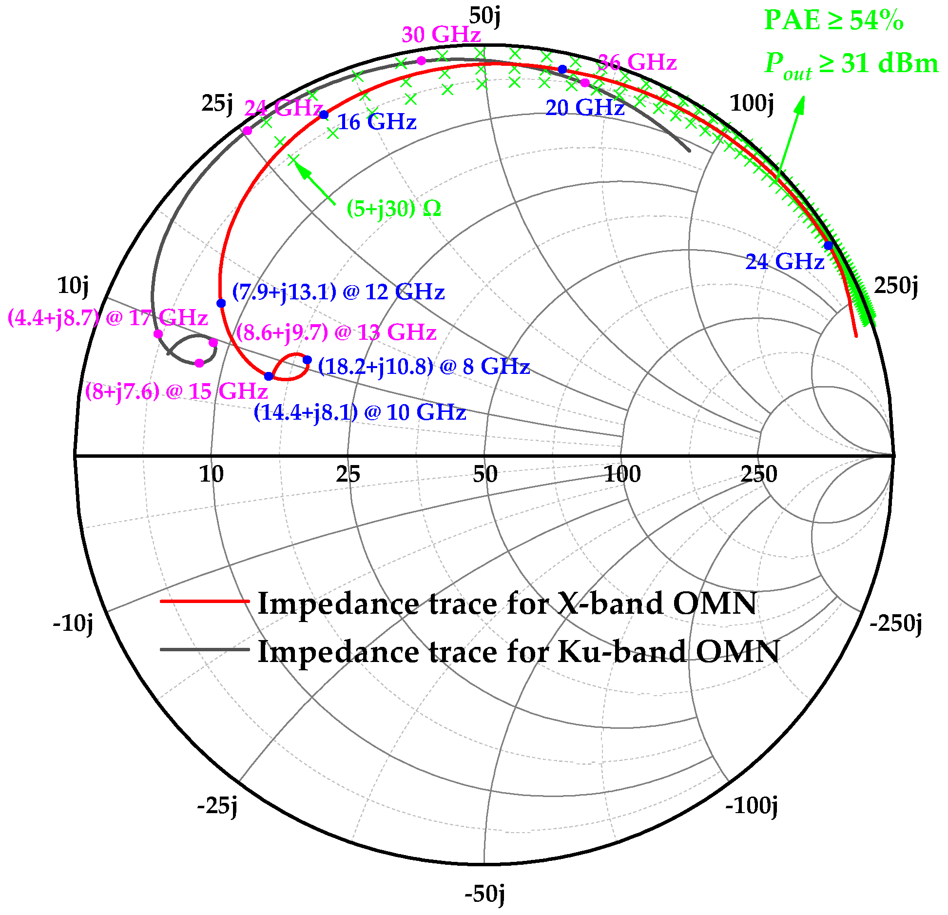
Figure 5 presents the simulated impedance traces of the output matching networks (OMNs) for the X band and Ku band. The highest efficiency and output power of the output-stage transistor are achieved when its second harmonic impedance is tuned to lie within the green region. Combined with Table 1, it can be seen that at both the frequency bands, the designed harmonic matching network can not only meet the second harmonic impedance control requirements but also satisfy the fundamental load matching requirements.

5. Design of the X and Ku Bands Class-J Power Amplifiers

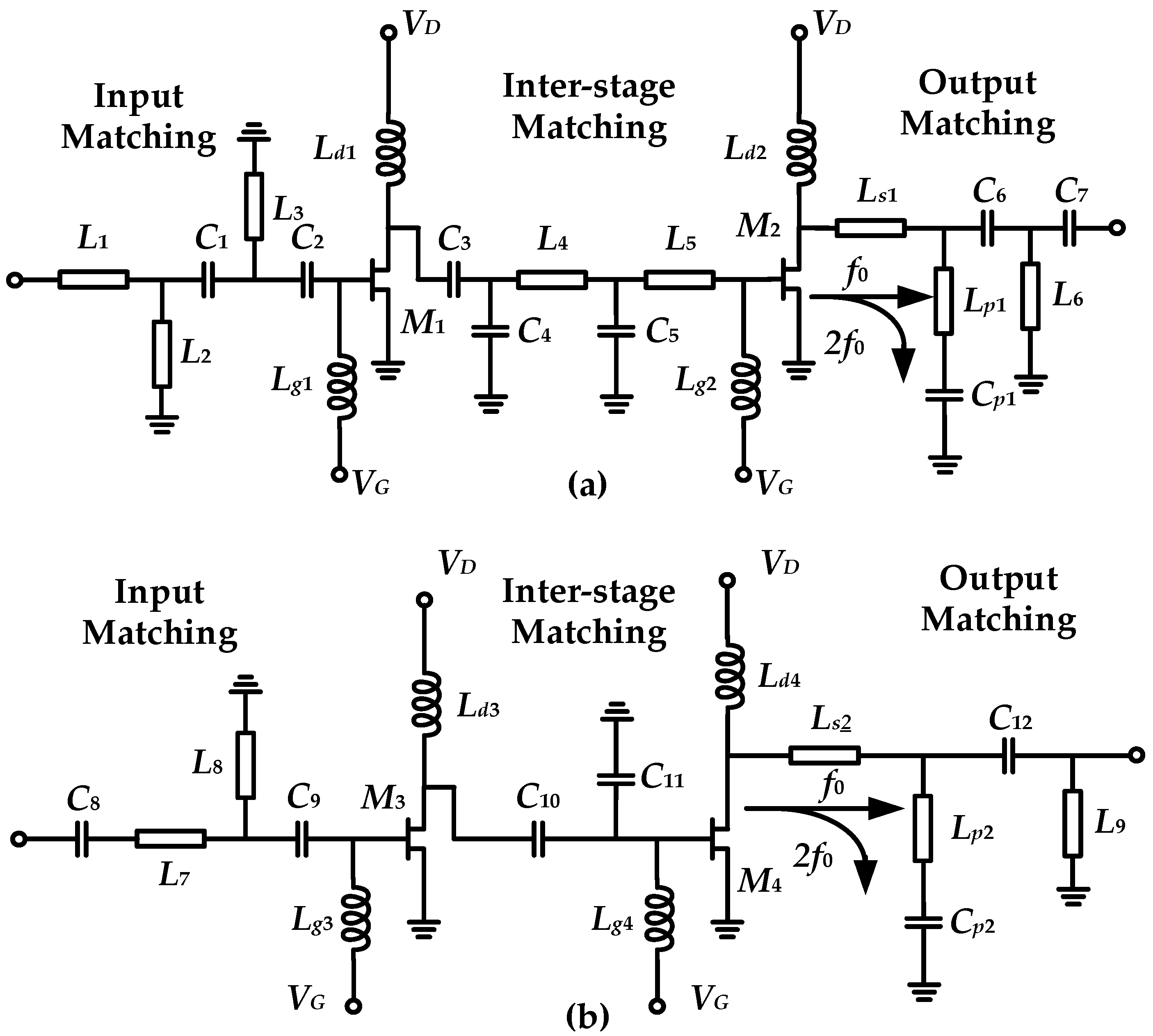
After completing the output impedance matching, the driver stages of the X-band and Ku-band amplifiers are designed. Figure 6 presents the schematic diagrams of the interstage and input matching networks, where Ld and Lg serve as the drain and gate bias lines, respectively. Table 2 shows the source-pull and load-pull results of the driver transistor. Combined with Zs of the output transistors in Table 1, the component values are optimized.
Figure 7 shows the optimized schematic diagrams of the proposed X-band and Ku-band power amplifiers. The optimized component values are provided in Table 3. Among them, some components are omitted as their minimal contribution to matching. All inductors are implemented using microstrip lines. Figure 8 presents the output-stage drain-source voltage and current waveforms of the amplifiers operating in the X and Ku bands. It can be observed that affected by the second harmonic, the peaks of the drain voltage all shift to the left, which is consistent with the characteristics of Class-J power amplifiers.

6. Simulated and Measured Results

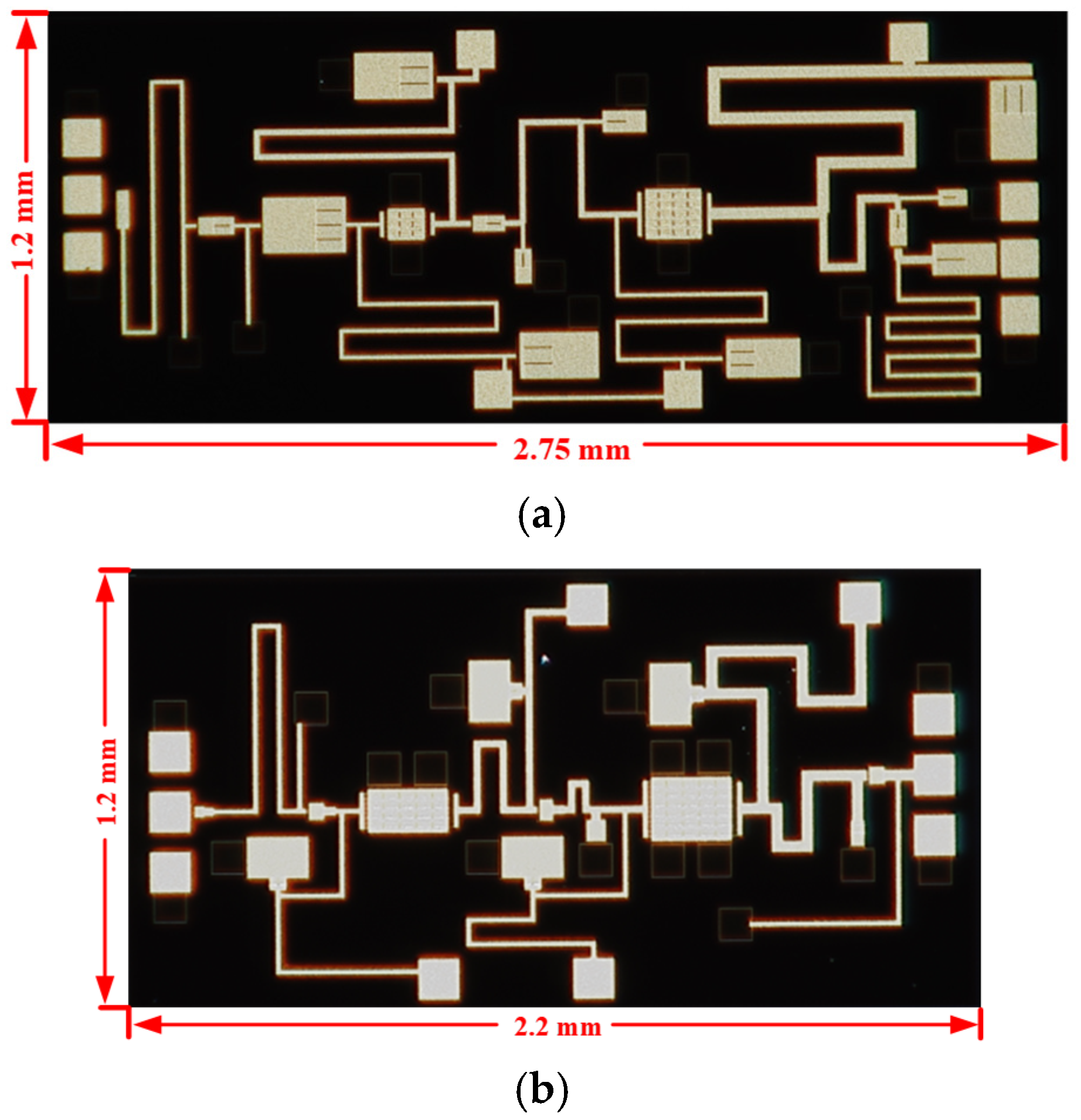
The two proposed continuous-mode power amplifiers are fabricated using a 0.25 mm GaAs pHEMT process. Figure 9 shows the microscope photographs of the two power amplifiers, with die areas of 2.75 mm × 1.2 mm and 2.2 mm × 1.2 mm, respectively. The S-parameters of the chips are measured using a Cascade Summit 1200 M probe station and a Keysight N5245A microwave network analyzer. Both chips undergo large-signal measurement after being eutectically bonded to a package with molybdenum-copper carriers, as shown in Figure 10. During the measurement, a heat sink is placed at the bottom to ensure efficient heat dissipation of the power amplifier chips.
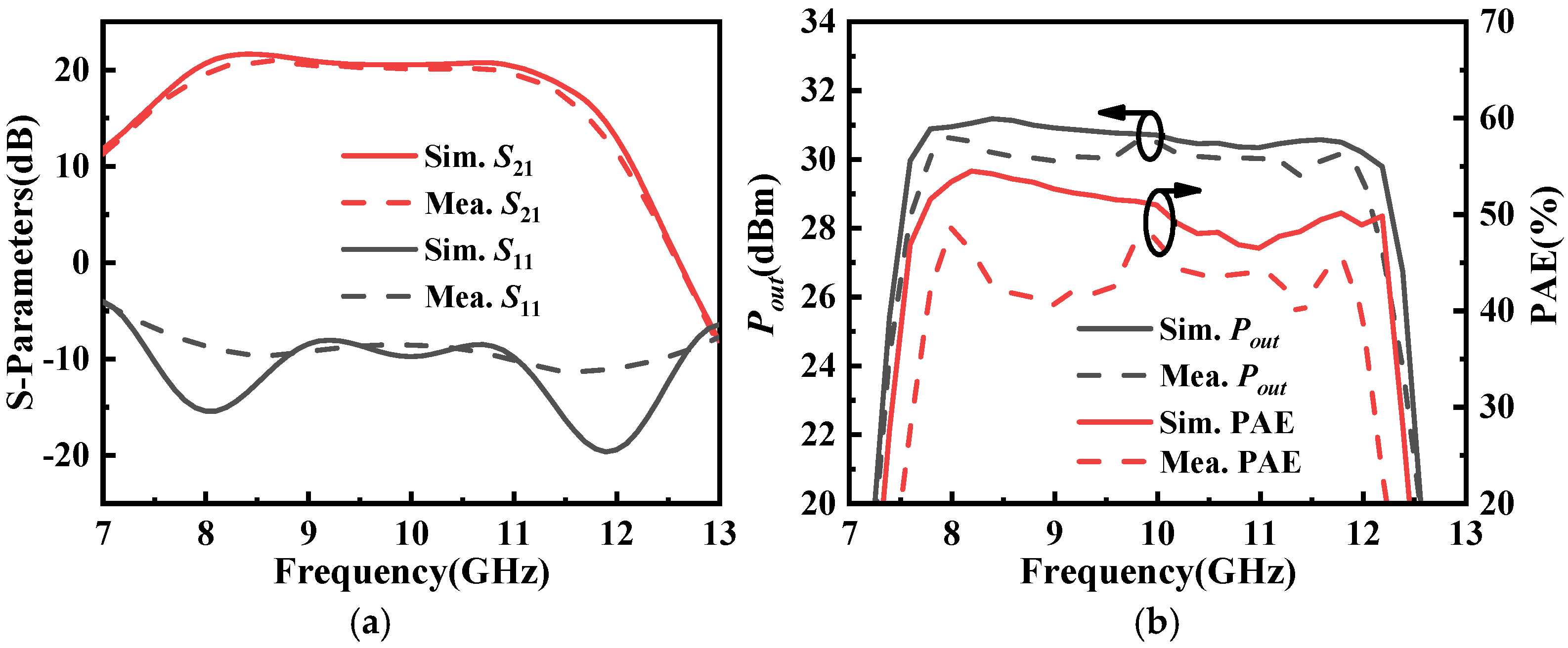
Figure 11a presents the S-parameter simulated and measured results of proposed X-band power amplifier. It can be observed that the simulated results are in good agreement with the measured results. Within the frequency range of 8 GHz to 12 GHz, the power amplifier achieves an average small-signal gain of approximately 20 dB, and the measured input reflection coefficient is better than −8 dB. Figure 11b shows the large-signal characteristic simulated and measured results. Within the operating frequency band, the power amplifier delivers a saturated output power exceeding 30 dBm, with a PAE higher than 39% across the band and a maximum of 48.5%.
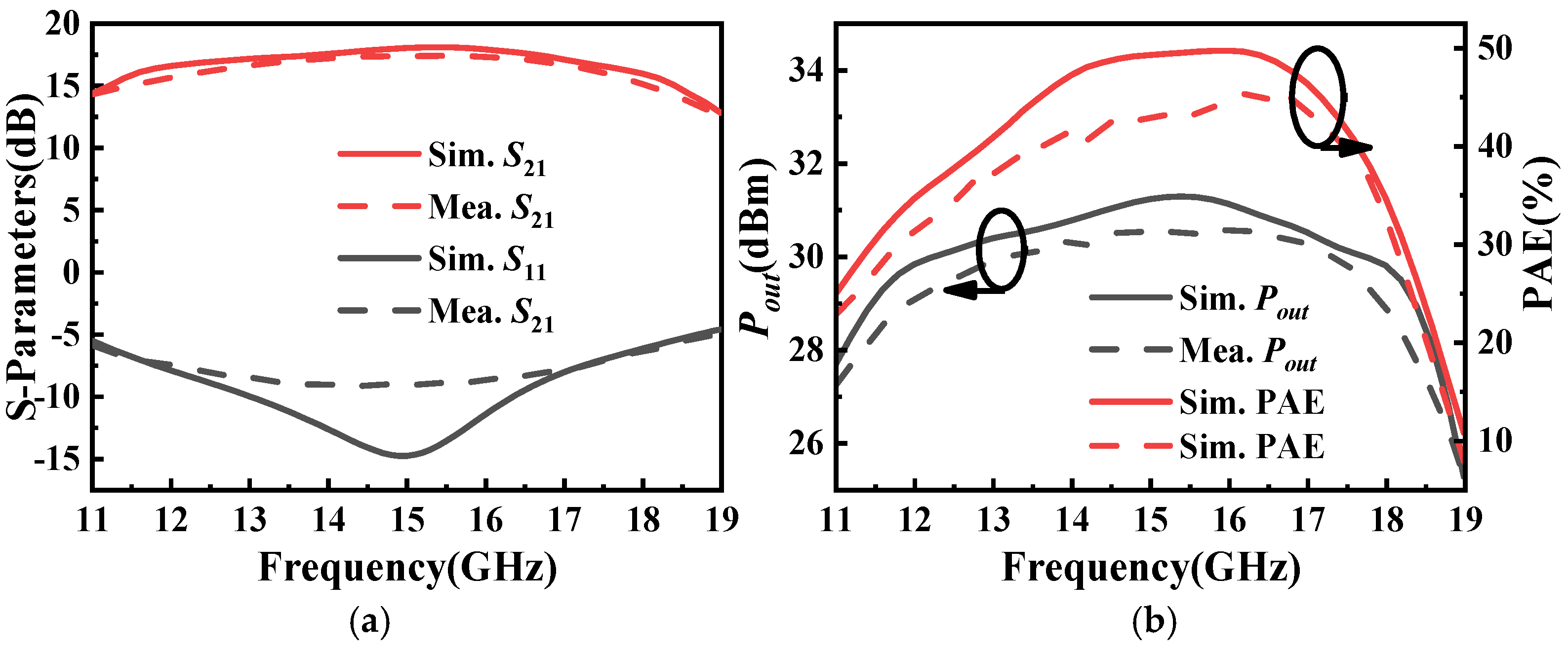
The simulated and measured results of the designed Ku-band power amplifier are shown in Figure 12. Over the frequency range of 12 GHz to 18 GHz, the power amplifier achieves an average small-signal gain of approximately 16.5 dB, and the measured input reflection coefficient is better than −6.3 dB. The measured saturated output power achieves an average of 30.8 dBm across the band and 29 dBm at the band edges. Meanwhile, the measured PAE within the band reaches a maximum of 45.3% and an average of 40.32%.
The detailed performance metrics of two fabricated power amplifiers are listed in Table 4 and compared with several similar GaAs-process-based power amplifier studies in the literature [12,13,14,15,16,17]. Compared with the power amplifiers in [12,13,16], the proposed design demonstrates a higher PAE under a comparable bandwidth. Although [14,15] achieve high efficiency by employing only fundamental load-pull techniques, they are narrowband. The well-engineered matching network in [17] enables excellent bandwidth but sacrifices PAE.
Table 4. Comparison with other similar research on power amplifiers in GaAs process.
Ref.TechnologyFrequency (GHz)BW
(%)
Psat *
(dBm)
PAE *
(%)
Area
(mm2)
[12]0.15-μm GaAs7~11.548.733.8433.6 × 1.8
[13]0.25-μm GaAs8~1347.631351 × 3.5
[14]0.25-μm GaAs8.5~11.53035493 × 1.8
[15]0.25-μm GaAs8.5~9.511.129.644.42 × 2
15.5~16.56.330.138.4
[16]0.25-μm GaAs11.7~17.640.33138.83.8 × 3.3
[17]0.25-μm GaAs6~1810040.5295 × 3.6
This work0.25-μm GaAs8~124031.2482.75 × 1.2
12~184030.845.32.2 × 1.2
* maximum values.

7. Conclusions

In this article, two wideband high-efficiency power amplifiers operating in the X and Ku bands, respectively, are designed and fabricated using a 0.25 µm-GaAs pHEMT process. A harmonic matching network is introduced in both power amplifiers, which extends the operating bandwidth without sacrificing efficiency. The proposed X-band power amplifier achieves a peak saturated output power of 31.2 dBm and a maximum PAE of 48%. The proposed Ku-band amplifier delivers a peak saturated output power of 30.8 dBm and a maximum PAE of 45.3%. Both chips feature a compact footprint, rendering them suitable for integration into miniaturized phased array T/R modules.

Author Contributions

Conceptualization, Y.Y. and Z.Y.; data curation, Y.Y., X.Z. and J.F.; funding acquisition, Z.Y.; methodology, Y.Y.; validation, Z.Y.; visualization, Z.Y.; writing—original draft, Y.Y. and X.Z.; writing—review and editing, Y.Y. All authors have read and agreed to the published version of the manuscript.

Funding

This work was supported by the Science and Disruptive Technology Research Fund Project of Aerospace Information Research Institute, Chinese Academy of Sciences (2024-AIRCAS-SDTP-02).

Data Availability Statement

The data presented in this study are available on request from the corresponding author due to (specify the reason for the restriction).

Conflicts of Interest

The authors declare no conflicts of interest.

References

  1. Maini, A.K. Handbook of Defence Electronics and Optronics: Fundamentals, Technologies and System; John Wiley & Sons: Hoboken, NJ, USA, 2018. [Google Scholar]
  2. Batra, J.; Balakrishnan, G.; Aiello, R.; Foerster, J.R.; Dabak, A. Design of a multiband OFDM system for realistic UWB channel environments. IEEE Trans. Microw. Theory Techn. 2004, 52, 2123–2138. [Google Scholar] [CrossRef]
  3. Cripps, S.C.; Tasker, P.J.; Clarke, A.L.; Lees, J.; Benedikt, J. On the continuity of high efficiency modes in linear RF power amplifiers. IEEE Microw. Wirel. Compon. Lett. 2009, 19, 665–667. [Google Scholar] [CrossRef]
  4. Chu, C.; Sharma, T.; Dhar, S.K.; Darraji, R.; Wang, X.; Pang, J.; Zhu, A. Waveform engineered sequential load modulated balanced amplifier with continuous class-F 1 and class-J operation. IEEE Trans. Microw. Theory Tech. 2021, 70, 1269–1283. [Google Scholar] [CrossRef]
  5. Xuan, X.; Cheng, Z.; Zhang, Z.; Le, C. Highly efficient ultrawideband power amplifier based on a novel multi-branch matching network. IEEE Microw. Wirel. Technol. Lett. 2023, 33, 1325–1328. [Google Scholar] [CrossRef]
  6. Alizadeh, A.; Hassanzadehyamchi, S.; Medi, A.; Kiaei, S. An X-band class-J power amplifier with active load modulation to boost drain efficiency. IEEE Trans. Circuits Syst. I Regul. Pap. 2020, 67, 3364–3377. [Google Scholar] [CrossRef]
  7. Gong, T.; Cheng, Z.; Zheng, B.; Xuan, X.; Le, C.; Fan, W.; Zhang, Z. SC band wideband GaN power amplifier MMIC for radar application. IEICE Electron. Express 2024, 21, 20240596. [Google Scholar] [CrossRef]
  8. Wright, P.; Lees, J.; Tasker, P.J.; Benedikt, J.; Cripps, S.C. An Efficient, Linear, Broadband Class-J-Mode PA Realised Using RF Waveform Engineering. In Proceedings of the 2009 IEEE MTT-S International Microwave Symposium Digest, Boston, MA, USA, 7–12 June 2009; IEEE: New York, NY, USA, 2009; pp. 653–656. [Google Scholar]
  9. Alizadeh, A.; Hassanzadehyamchi, S.; Medi, A. Integrated output matching networks for class–J/J− 1 power amplifiers. IEEE Trans. Circuits Syst. I Regul. Pap. 2019, 66, 2921–2934. [Google Scholar] [CrossRef]
  10. Kazimierczuk, M.K. RF Power Amplifiers; John Wiley & Sons: Hoboken, NJ, USA, 2014. [Google Scholar]
  11. Sheikhi, A.; Hemesi, H. Analysis and design of the novel class-F/E power amplifier with series output filter. IEEE Trans. Circuits Syst. II Express Briefs 2021, 69, 779–783. [Google Scholar] [CrossRef]
  12. Li, J.; Yuan, Y.; Yuan, B.; Tan, C.; Yu, Z. Analysis and design of broadband 2-W power amplifier based on cascode transistors. Microw. Opt. Technol. Lett. 2024, 66, e34205. [Google Scholar] [CrossRef]
  13. Babakrpur, E.; Medi, A.; Namgoong, W. Wideband GaAs MMIC driver power amplifiers for X and Ku bands. In Proceedings of the 2017 Texas Symposium on Wireless and Microwave Circuits and Systems (WMCS), Waco, TX, USA, 30–31 March 2017; IEEE: New York, NY, USA, 2017; pp. 1–4. [Google Scholar]
  14. Hua, Y.; Wu, H.; Liao, X.; Liao, C.; Hu, L.; Lv, J. A High-Efficiency 3-Watt GaAs pHEMT X-Band MMIC Power Amplifier. In Proceedings of the 2018 International Conference on Microwave and Millimeter Wave Technology, Chengdu, China, 7–11 May 2018; IEEE: New York, NY, USA, 2018; pp. 1–2. [Google Scholar]
  15. Xie, C.; Wu, P.; Tan, C.; Yuan, Y.; Zeng, J.; Yu, Z. An X/Ku dual-band switchless frequency reconfigurable GaAs power amplifier. IEEE Microw. Wirel. Compon. Lett. 2022, 32, 539–542. [Google Scholar] [CrossRef]
  16. Yao, G.; Jia, H.; Zhao, Z.; Lu, Y.; Yi, C.; Liu, X.; Feng, T.; Yang, L.A.; Ma, X. A Ku-Band Broadband High-Efficiency GaAs MMIC Power Amplifier. In Proceedings of the 2024 International Conference on Microwave and Millimeter Wave Technology (ICMMT), Beijing, China, 16–19 May 2024; IEEE: New York, NY, USA, 2024; Volume 1, pp. 1–3. [Google Scholar]
  17. Meghdadi, M.; Medi, A. Design of 6–18-GHz high-power amplifier in GaAs pHEMT technology. IEEE Trans. Microw. Theory Tech. 2017, 65, 2353–2360. [Google Scholar] [CrossRef]
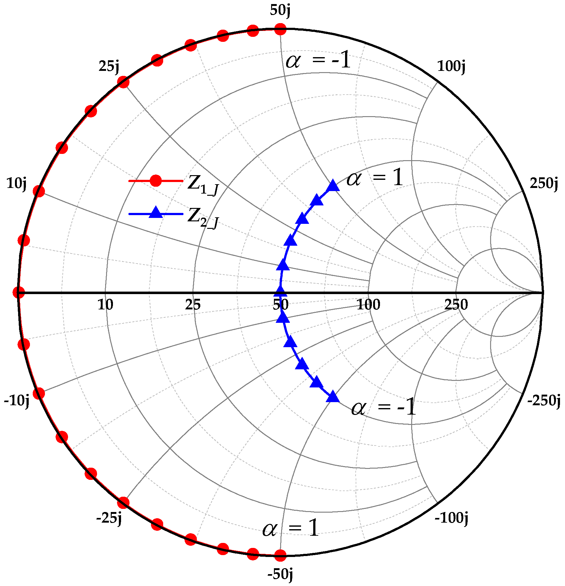
Figure 1. The normalized impedance traces of Zn_J with different values of a.
Micromachines 16 01362 g001
Figure 2. The waveforms of vd_J and id_J for different values of a.
Micromachines 16 01362 g002
Figure 3. The simulated results of Psat and PAE at different values of Imload2.
Micromachines 16 01362 g003
Figure 4. The schematic diagram of the (a) designed harmonic matching network and (b) its fundamental equivalent circuit.
Micromachines 16 01362 g004
Figure 5. The simulated impedance traces of the OMNs for the X band and Ku band.
Micromachines 16 01362 g005
Figure 6. The schematic diagrams of the (a) inter-stage and (b) input matching networks.
Micromachines 16 01362 g006
Figure 7. The schematic diagrams of the designed power amplifiers at (a) X band and (b) Ku band.
Micromachines 16 01362 g007
Figure 8. The output-stage voltage and current waveforms of the amplifiers operating at (a) 10 GHz and (b) 14 GHz.
Micromachines 16 01362 g008
Figure 9. The microscope photograph of the designed continuous-mode power amplifiers for (a) the X band and (b) the Ku band.
Micromachines 16 01362 g009
Figure 10. The mearsured carrier for the amplifier chips.
Micromachines 16 01362 g010
Figure 11. The simulated and measured results of the designed X-band power amplifier: (a) S-parameters and (b) large-signal characteristics.
Micromachines 16 01362 g011
Figure 12. The simulated and measured results of the designed Ku-band power amplifier: (a) S-parameters and (b) large-signal characteristics.
Micromachines 16 01362 g012
Table 1. The results of source pull and harmonic load pull for the output-stage transistors of the X-band and Ku-band power amplifiers.
Frequency8 GHz10 GHz12 GHz
Zs(11.9 + j21.5) Ω(5.2 + j15) Ω(5.8 + j14.3) Ω
Zf0(18.5 + j11.6) Ω(14.6 + j9.1) Ω(10.1 + j10.4) Ω
Z2f0>j30 W>j30 W>j30 W
Frequency13 GHz15 GHz17 GHz
Zs(7.3 + j10.8) Ω(6.3 + j2.4) Ω(3.1 + j1.7) Ω
Zf0(8.9 + j9.5) Ω(7.8 + j8.1) Ω(6.1 + j8.5) Ω
Z2f0>j30 W>j30 W>j30 W
Table 2. The results of source pull and load pull for the driver transistors of the X band and Ku band.
Frequency8 GHz10 GHz12 GHz
Zs(17.4 + j16) Ω(15.2 + j14.5) Ω(13.9 + j12.1) Ω
ZL(31.3 + j28.5) Ω(29.5 + j26) Ω(28.6 + j23) Ω
Frequency13 GHz17 GHz15 GHz
Zs(2.4 + j4.6) Ω(2 + j5.2) Ω(2 + j4.3) Ω
ZL(9.3 + j14.6) Ω(7.1 + j12) Ω(3.9 + j13) Ω
Table 3. The optimized component values shown in Figure 6.
ComponentsValuesComponentsValues
L110 mm × 1500 μmC120.52 pF
L210 mm × 340 μmLg110 mm × 1550 μm
L310 mm × 300 μmLg210 mm × 1400 μm
L415 mm × 400 μmLg310 mm × 900 μm
L515 mm × 300 μmLg410 mm × 1000 μm
L610 mm × 1800 μmLd115 mm × 1350 μm
L710 mm × 1050 μmLd230 mm × 1600 μm
L810 mm × 250 μmLd315 mm × 650 μm
L910 mm × 800 μmLd430 mm × 1100 μm
C10.67 pFLs120 mm × 450 μm
C26.10 pFLs230 mm × 400 μm
C30.52 pFLp110 mm × 160 μm
C40.62 pFLp230 mm × 120 μm
C51.01 pFCp10.39 pF
C60.68 pFCp20.35 pF
C72.30 pFM16 × 100 μm
C80.19 pFM210 × 150 μm
C90.52 pFM38 × 200 μm
C100.56 pFM412 × 200 μm
C110.83 pF
Disclaimer/Publisher’s Note: The statements, opinions and data contained in all publications are solely those of the individual author(s) and contributor(s) and not of MDPI and/or the editor(s). MDPI and/or the editor(s) disclaim responsibility for any injury to people or property resulting from any ideas, methods, instructions or products referred to in the content.