Highlights
- Monolithic inverters of CMOS-HEMTs consisting of D- and E-mode GaN-based devices were fabricated.
- Characteristics of GaN-based MOS-HEMTs were influenced by the source field plate length.
- Double-2DEG channels and fin-gated multiple nanochannels enhanced the device’s characteristics.
Abstract
In this study, enhancement- and depletion-mode (E- and D-mode) GaN-based 120 nm-wide fin-gated multiple nanochannel metal–oxide–semiconductor high-electron-mobility transistors (MOS-HEMTs) were manufactured on the epitaxial Al0.83In0.17N/GaN/Al0.18Ga0.82N/GaN two-dimensional electron gas (2DEG) channel layers grown on Si substrates using a metal-organic chemical vapor deposition system. The oxide layer grown directly by the photoelectrochemical oxidation method was used as the gate oxide layer in D-mode MOS-HEMTs. Furthermore, E-mode MOS-HEMTs used ferroelectric stacked LiNbO3/HfO2/Al2O3 layers as the gate oxide layers. The 120 nm-wide multiple nanochannels and various-length source field plates (SFPs) were fabricated and incorporated into monolithic complementary MOS-HEMTs (CMOS-HEMTs) consisting of D- and E-mode MOS-HEMTs. The resulting monolithic unskewed inverter was achieved by modulating the drain-source current of the D-mode MOS-HEMTs. The noise low margin of 2.03 V and noise high margin of 2.10 V of the unskewed monolithic inverter were obtained. From the dynamic experimental results, the rising time and falling time of the unskewed monolithic inverter were 4.9 μs and 3.2 μs, respectively. The breakdown voltage could be improved by incorporating an SFP. When the SFP edge was located at the center between the gate electrode and the drain electrode, the maximum breakdown voltage of 855 V was obtained.
1. Introduction
Recently, owing to significant advances in epitaxial growth, manufacturing, and design techniques, gallium nitride (GaN)-based semiconductors have been successfully employed to fabricate various GaN-based high-electron-mobility transistors (HEMTs) and to apply them in practical systems [1,2,3,4]. To increase the drain-source current (IDS) and thus boost device power, one effective method is to simultaneously improve both the sheet electron density and the electron mobility in the two-dimensional electron gas (2DEG) channel induced at the interface between the hetero-structured AlGaN and GaN layers. Among them, one method is to use complex epitaxial growth techniques to grow an AlGaN barrier layer with a higher Al content on the GaN channel layer. While this method can increase the sheet electron density in the 2DEG channel, it also reduces its electron mobility [5]. In recent years, multiple 2DEG channels have been epitaxially grown and used to fabricate depletion-mode (D-mode) and enhancement-mode (E-mode) GaN-based planar HEMTs, thereby overcoming the challenges [6,7,8]. Because the lattice-matched hetero-structured 2DEG channel structures can mitigate the failure induced by the inverse piezoelectric effect of the strain, the lattice-matched AlInGaN/GaN hetero-structured layers were grown and utilized for fabricating GaN-based HEMTs [9,10]. The epitaxial layers of the double-2DEG channels of the Al0.83In0.17N/GaN/Al0.18Ga0.82N/GaN were grown on silicon (Si) substrates using a metal-organic chemical vapor deposition system (AIXTRON Group, Herzogenrath, Germany) and were used to fabricate D-mode GaN-based metal-oxide-semiconductor HEMTs (MOS-HEMTs) previously [11,12]. Due to the superior gate control capability of the fin-gate structure, GaN-based MOS-HEMTs with fin-gated multiple nanochannels exhibited higher performance than that of the planar devices [12,13,14]. Moreover, field plate engineering has been employed to improve breakdown characteristics, alleviate current collapse, and mitigate dynamic degradation by tailoring the electric field profiles and potential lines [15,16,17]. The literature already contained a considerable number of planar GaN-based D- and E-mode HEMTs that utilized various structures and manufacturing processes. Even fin-gated multiple nanochannel ones were recently developed and investigated. However, those devices were almost manufactured using a single-2DEG channel epitaxial structures. In this study, double-2DEG channels of the epitaxial Al0.83In0.17N/GaN/Al0.18Ga0.82N/GaN layers were grown. The D- and E-mode GaN-based fin-gated multiple nano MOS-HEMTs were fabricated using the epitaxial layers. Furthermore, various source field plates were introduced in the D- and E-mode devices. In this study, by integrating SFP-incorporated D- and E-mode MOS-HEMTs with double-2DEG channels and fin-gated multiple nanochannels to form complementary MOS-HEMTs (CMOS-HEMTs), the resulting monolithic inverters were also fabricated, measured, and analyzed. Furthermore, to explore the affected functions and characteristics, various-length SFPs were designed and manufactured.
2. Monolithic Inverters Fabrication Process
The schematic configuration of the cross-sectional and the associated equivalent circuit of the monolithic inverters were respectively illustrated in Figure 1a,b. The E-mode device and the D-mode device worked in driver and load roles, respectively, for the monolithic inverter. The epitaxial layers were grown on a Si substrate using a metal-organic chemical deposition system. The used Si substrates were 6-inch and 1000 μm-thick Boron-doped p-type Si wafers with [111]-orientation and resistivity of 3 Ω-cm. The wafers were manufactured by Wafer Works Company. The epitaxial growth processes, high-resolution transmission electron microscopy, and simulated band diagram and electron concentration distribution of the epitaxial layers were reported previously [11]. The double-2DEG channels were formed by the band-discontinued lattice-matched Al0.83In0.17N (8 nm)/GaN (10 nm) layers and the polarized Al0.18Ga0.82N (25 nm)/GaN (100 nm) layers, respectively. The double-2DEG channels are marked in Figure 1a. Using a Hall measurement at room temperature, the total sheet electron density and the equivalent electron mobility were measured to be 1.1 × 1013 cm−2 and 1770 cm2/Vs, respectively.
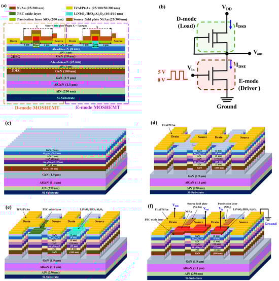
Figure 1.
(a) Cross-sectional configuration and (b) equivalent circuit of source field plate incorporated monolithic inverters, and three-dimensional configuration of (c) multiple nanochannel structure, (d) source and drain electrode’s structure, (e) gate oxide layers, and (f) source field plate incorporated monolithic inverters.
After spring positive photoresist CSAR62 onto the epitaxial wafer, an electron-beam lithography system (ELS-BODEN 50, ELIONIX Inc., Tokyo, Japan) was used to pattern parallel straight multiple nanochannels. The channel width and channel spacing were 120 nm and 880 nm, respectively. When a 50 nm-thick Ni mask was deposited using an electron beam evaporator, the multiple nanochannels were then fabricated using an inductively coupled plasma system with a mixed boron trichloride and chlorine etchant gas. By removing the Ni metal mask using a hydrochloric acid (HCl) chemical solution, the resulting multiple nanochannels were illustrated in Figure 1c. An electron beam evaporator was used to deposit a 50 nm-thick Ni metal on the window of mesa isolation regions patterned by a standard photolithography method. After a lift-off process of the undesired metal, the mesa isolation regions were formed by using the mixed etchant gases under the protection of the patterned Ni metal mask. After the patterned Ni metal mask was removed using a HCl chemical solution, the windows of the source region and drain region were opened using a standard photolithography method. Ti/Al/Pt/Au (25/100/50/300 nm) metals for the source and drain electrodes of D- and E-mode MOS-HEMTs were deposited using an electron-beam evaporator and then annealed in a nitrogen ambient at 900 °C for 30 s. The source and drain electrodes were separated by 10 μm. Figure 1d shows the resulting figuration. Using a standard photolithography system to open 2 μm-wide straight gate windows of the D-mode device. The gate oxide layer and the gate-recessed structure were simultaneously obtained using the previously reported photoelectrochemical (PEC) oxidation method [18,19]. This directly grown gate oxide layer surrounded the top and two sidewalls of the nanochannels, forming fin-gated channels for the D-mode MOS-HEMTs. By controlling the PEC process time, the recessed gate depth of the D-mode MOS-HEMT could be adjusted, thereby adjusting the drain-source current to the required value. In this study, the depths were 6 nm, 7 nm, and 8 nm, respectively. To stabilize the gate oxide layers, they were converted into mixed crystalline α-Al2O3 and β-Ga2O3 materials by annealing them in an oxygen ambient at 700 °C for 2 h [20]. The distance between the gate electrode and the source electrode, and the distance between the gate electrode and the drain electrode were 4 μm, respectively. To fabricate the gate of E-mode MOS-HEMTs, the 2 μm-wide straight windows were opened using a standard photolithography system. After the gate-recessed regions with a depth of 6 nm were created using the previously reported PEC etching method [21], an atomic layer deposition system was utilized to first deposit Al2O3 tunneling layer (10 nm) and HfO2 charge storage layer (4 nm), and then Krypton fluoride pulsed laser system was used to deposit LiNbO3 ferroelectric blocking layer (40 nm) sequentially. The ferroelectric stacked LiNbO3/HfO2/Al2O3 gate oxide layers surrounded the top and two sidewalls of the nanochannels, forming fin-gated channels for the E-mode MOS-HEMTs. To partially compensate for the electrons in the 2DEG channels, the strong (006) crystalline ferroelectric phase of the LiNbO3 film, which has the upward C+ domain polarization and opposite to the polarization direction of the 2DEG channels, was obtained by annealing in an oxygen ambient at 600 °C for 30 min. The X-ray diffraction pattern and the vertical piezoelectric force microscopy images of the LiNbO3 films were reported previously [22]. The resulting configuration was illustrated in Figure 1e. Using a standard photolithography method to open the windows for the gate regions of D- and E-mode MOS-HEMTs and the connection electrodes among the gate and source of the D-mode MOS-HEMTs and the drain of the E-mode MOS-HEMT, Ni/Au (25/200 nm) metals were deposited using an electron-beam evaporator. To incorporate various SFPs onto both the D-mode device and E-mode device, a SiO2 passivation layer (200 nm) was deposited on the photolithographic pattern windows between the source and drain electrodes using a plasma-enhanced chemical deposition system. After patterning the SFP region, Ni/Au (25/300) metals were deposited, and the unnecessary Ni/Au metals were lifted off. The SFPs were incorporated into the D-mode device and E-mode device of the monolithic inverters. The resulting configuration was shown in Figure 1f. To explore the dependence of the drain-source breakdown voltage on the edge location of SFP, 7, 8, and 9 μm-length SFPs were designed and fabricated. In this study, the distance between the source and drain electrodes was 10 μm, and the 2 μm-wide gate electrode was located in the center between them. Therefore, the edges of 7, 8, and 9 μm-length SFPs were located near the gate electrode, in the center between the gate electrode and drain electrode, and near the drain electrode. In Figure 1f, in addition to showing that the Ni/Au electrode connected the gate and source of the D-mode device to the drain of the E-mode device, the input voltage (Vin), output voltage (Vout), and ground of the monolithic inverter were also indicated.
3. Experimental Results and Discussion
The direct-current (DC) characteristics of the D- and E-mode MOS-HEMTs in the monolithic inverter were respectively measured using an Agilent 4156C semiconductor parameter analyzer. Figure 2 shows the drain-source current (IDSD)—gate-source voltage (VGSD) characteristics and the transconductance (gmD)—VGSD characteristics of the D-mode MOS-HEMT with a recessed-gate depth of 6 nm. The drain-source current was the measured drain-source current normalized with the effective channel width. When the threshold voltage was defined as the VGSD corresponding to the IDSD of 0.1 mA/mm, the threshold voltage (VthD) of the D-mode MOS-HEMTs was approximately −1.9 V. The maximum transconductance (gmD,max) was approximately 125 mS/mm. When the VGSD was 5 V, the IDSD of the D-mode MOS-HEMTs operating at VDSD of 5 V was 801.3 mA/mm. The inset of Figure 2 shows the associated IDSD—drain-source voltage (VDSD) characteristics of the D-mode MOS-HEMTs with recessed-gate depths of 6, 7, and 8 nm. Under the VDSD = 5 V and VGSD = 0 V, the D-mode MOS-HEMTs with recessed-gate depths of 6 nm, 7 nm, and 8 nm exhibited IDSD of 27.3 mA/mm, 19.6 mA/mm, and 13.6 mA/mm, respectively. After the E-mode MOS-HEMT was initialized at a gate-source voltage (VGSE) of 12 V for 10 ms, Figure 3 shows the drain-source current (IDSE)—VGSE characteristics and the transconductance (gmE)—VGSE characteristics, and the inset shows the IDSE—VDSE characteristics. The threshold voltage (VthE) and maximum transconductance (gmE,max) of the E-mode MOS-HEMTs were approximately 2.3 V and 125.9 mS/mm, respectively. Under the operation of VDSE = 5 V and VGSE = 5 V, the IDSE was approximately 492.1 mA/mm.
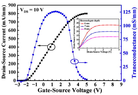
Figure 2.
Drain-source current and transconductance as a function of gate-source voltage of the D-mode MOS-HEMTs. Under VGS of 0 V, the inset figure was associated with IDSD—VDSD characteristics with recessed-gate depths of 6, 7, and 8 nm.
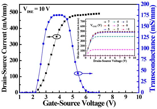
Figure 3.
Drain-source current and transconductance as a function of gate-source voltage of E-mode MOS-HEMTs. The inset figure was associated with IDSE—VDSE characteristics.
As the equivalent circuit of the monolithic inverter shown in Figure 1b, when the input voltage (Vin) with a 5-V-amplitude pulsed-rectangular waveform is biased to the gate of the E-mode MOS-HEMT, the output voltage (Vout) is obtained from the drain of the E-mode MOS-HEMT. To investigate the performance of the monolithic inverters, D-mode MOS-HEMTs with gate-recessed depths of 6 nm, 7 nm, and 8 nm were fabricated. When the monolithic inverter operated at VDD of 5 V and Vin of 5 V, because the gate and source of the D-mode MOS-HEMT were shorted (i.e, VGSD = 0 V), Figure 4 shows the load line curves of the monolithic inverters with the above-mentioned three D-mode MOS-HEMTs. The IDSE curve of the E-mode MOS-HEMT operated at VGSE = 5 V was also shown in Figure 4. To distinguish the D-mode MOS-HEMTs from the monolithic inverters, the drain-source current ratio (IDSE/IDSD) of the E- and D-mode MOS-HEMTs was defined as β. For the D-mode MOS-HEMTs fabricated with recessed-gate depths of 6 nm, 7 nm, and 8 nm, the associated β value was approximately 18.0, 25.1, and 36.2, respectively. As shown in Figure 4, the IDSE curve intersected the load line curves and created the intersection points that are the low output voltages (VOL) of the monolithic inverters. The VOL was 0.13 V, 0.08 V, and 0.07 V as β = 18.0, 25.1, and 36.2, respectively. The high output voltage (VOH) of the monolithic inverters was defined as Vout = VDD = 5 V. It was observed that the VOL decreased with increasing β value. By changing the amplitude of Vin from 0 to 5 V, the associated output voltage swing (VOS = VDD − VOL) was swept to 4.87 V, 4.91 V, and 4.93 V, respectively. The VOS increased with increasing the β value.
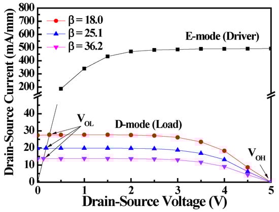
Figure 4.
Load lines of monolithic inverters with various β values.
The static voltage transfer characteristics (SVTC) of the monolithic inverters with different β values are shown in Figure 5. The low input voltage (VIL) and high input voltage (VIH) were defined as the Vin and Vout, corresponding to a tangent slope of −1 of the SVTC. Table 1 lists the calculated data. Except for the VOH that remained at 5.0 V, the values of the other VIL, VIH, and VOL decreased as the β value increased. In addition, to investigate the tolerable noise variation range within which the monolithic inverters with different values would not produce logic errors, the noise low margin (NML = VIL − VOL) and noise high margin (NMH = VOH − VIH) were evaluated and are listed in Table 1. The NML and NMH values were increased with an increase in β. When Vout = VDD/2 = 2.5 V, the Vin was 2.61 V, 2.51 V, and 2.45 V as β = 18.0, 25.1, and 36.2, respectively. In general, when Vout was VDD/2, the monolithic inverter exhibited optimal unskewed behaviors when Vin was also VDD/2. It could be deduced that the optimal unskewed inverter could be achieved as β of 25.1. Comparing the NMH and NML of the monolithic inverters with β of 18.0, 25.1, and 36.2, the monolithic inverter with β of 18.0 has greater symmetry between the NMH and NML. Although there is an imbalance in symmetry between the NMH (2.10 V) and NML (2.03 V), the characteristic of exceeding 2 V can still effectively overcome the noise variations in the unskewed monolithic inverter with β of 25.1. Figure 6 shows the Vout—Vin dynamic characteristics of the monolithic inverter with β of 25.1. The rising time of 4.9 μs and the falling time of 3.2 μs indicated that the monolithic inverters could operate at a higher switch speed.
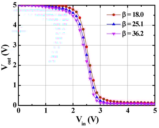
Figure 5.
Static voltage transfer characteristics of monolithic inverters with various β values.

Table 1.
Characteristics of monolithic inverters with various β values.
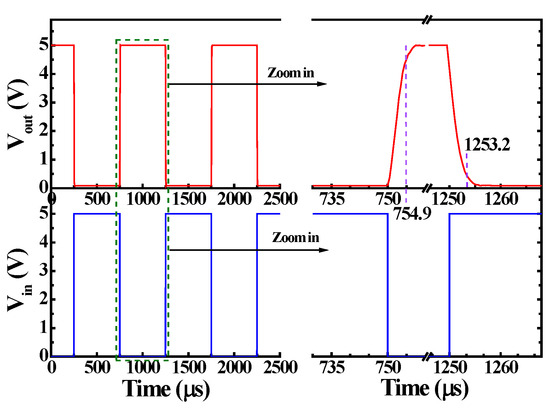
Figure 6.
Vout—Vin dynamic characteristics of unskewed monolithic inverter.
To explore the dependence of the breakdown voltage on the SFP length, the breakdown voltages of the various monolithic inverters were measured. Compared with the breakdown voltage of 746 V without an SFP, breakdown voltages of 780 V, 855 V, and 821 V were obtained by incorporating 7, 8, and 9 μm-length SFPs, respectively. It is worth noting that the breakdown voltage was improved by incorporating the SFP. However, the improved breakdown voltage was still affected by the SFP length. To explore the simulated electric field distribution along the 2DEG channels using various-length SFPs, simulations were carried out using the NTU DDCC TCAD platform, where the Poisson and drift–diffusion equations were solved self-consistently with a two-dimensional finite element method (2D FEM). Figure 7 shows the simulated electric field distributions without and with 7, 8, and 9 μm-length SFPs operating at a VDS of 600 V. The simulated electric field profiles show that MOS-HEMTs without an SFP exhibit a pronounced peak near the gate electrode, which makes them more prone to premature breakdown. Introducing an SFP redistributes the electric field and reduces the peak electric field intensity, thereby enhancing breakdown voltage. The impact of SFP length is equally critical in determining the electric field distribution and breakdown voltage. The simulations show that a 7 µm SFP, although capable of reducing the gate-side peak compared to the case without the SFP, still produces significantly high residual peaks. This is because the SFP is too short to sufficiently spread the potential toward the drain, leaving the electric field concentrated near the gate region. In contrast, the 8 µm field plate achieves the most balanced redistribution. The first peak near the gate is effectively suppressed, and the second peak toward the drain side remains moderate. As a result, the 8 µm design consistently yields the highest breakdown voltage. When the SFP length is further increased to 9 µm, the redistribution becomes excessive, pushing the depletion region too close to the drain contact. This leads to a re-enhanced local peak at the SFP edge, which can even exceed the values observed in the 7 µm case, thereby reducing the effectiveness of breakdown improvement.
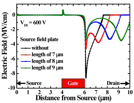
Figure 7.
Simulated electric field distributions without and with various lengths of source field plates.
4. Conclusions
In this study, D- and E-mode GaN-based 120 nm-wide fin-gated multiple nanochannel MOS-HEMTs were fabricated on the epitaxial double-2DEG channel layers. To explore the affected functions and characteristics, various-length SFPs were introduced into the D- and E-mode MOS-HEMTs. By integrating D- and E-mode MOS-HEMTs, the monolithic inverters with CMOS-HEMT architecture were obtained. To control the drain-source current of the D-mode MOS-HEMT to obtain a β value of 25.1 in monolithic inverters, the performance of unskewed inverters was achieved. In the unskewed inverters, the NML and NMH were 2.03 V and 2.10 V, respectively. It indicated that the unskewed monolithic inverters could tolerate noise variations of more than 2 V. Furthermore, the dynamic experimental results, based on a rising time of 4.9 μs and a falling time of 3.2 μs, verified that the unskewed monolithic inverter could operate at high switch speed. Using the TCAD simulation, the highest breakdown voltage was achieved when the SFP edge was located at the center between the gate and the drain. It was found that the unskewed monolithic also could work at a high breakdown voltage of 855 V. Table 2 lists the comparison results of inverters [23,24,25,26,27,28,29]. The studied monolithic inverters have promising superior characteristics. Although the impact of the SFP on the monolithic inverters was simulated and demonstrated, the structure and dimension of the optimal SFPs based on the thickness and properties of the passivation layer and the structure and geometry of the D- and E-mode MOS-HEMTs are still being simulated and designed in detail. In this study, the performance of the SFP incorporated monolithic inverters was demonstrated. To achieve optimal unique performance for various monolithic inverters, different SFP structures are expected. In this study, the functions and improved characteristics of source field plates are incorporated into the monolithic inverters. Because specific characteristics of the source field plate, gate field plate, drain field plate, and multiple field plates can improve the different characteristics. Therefore, by standing the different geometries and various field plates in the monolithic inverters, the characteristics of the resulting monolithic inverters can be enhanced.
Table 2.
Comparison data of inverters.
Author Contributions
Conceptualization, H.-Y.C. and C.-T.L.; data curation, H.-Y.C. and H.-Y.L.; software, H.L. and Y.-R.W.; funding acquisition, C.-T.L. and H.-Y.L.; investigation, H.-Y.C., H.-Y.L., and C.-T.L.; writing—original draft, C.-T.L.; writing—review and editing, H.-Y.L. and C.-T.L. All authors have read and agreed to the published version of the manuscript.
Funding
This work was supported by the National Science and Technology Council (NSTC), Republic of China, under Grants NSTC 113-2221-E-006-106-MY3, NSTC 113-2923-E-006-012, NSTC 114-2221-E-006-200-MY3, NSTC 114-2221-E-006-043, and NSTC 114-2218-E-006-006.
Data Availability Statement
The original contributions presented in this study are included in the article. Further inquiries can be directed to the corresponding author.
Acknowledgments
The authors gratefully acknowledge Taiwan Semiconductor Research Institute (TSRI) and the use of the instruments belonging to the Core Facility Center of National Cheng Kung University.
Conflicts of Interest
The authors declare no conflicts of interest.
References
- Greco, G.; Iucolano, F.; Roccaforte, F. Review of technology for normally-off HEMTs with p-GaN gate. Mater. Sci. Semicond. Process. 2018, 78, 96–106. [Google Scholar] [CrossRef]
- Lee, C.T.; Chen, W.S.; Lee, H.Y. Quadruple gate-embedded T structured GaN-based metal–oxide–semiconductor high-electron mobility transistors. IEEE J. Electron Devices Soc. 2018, 6, 63–67. [Google Scholar] [CrossRef]
- Haziq, M.; Falina, S.; Manaf, A.A.; Kawarada, H.; Syamsul, M. Challenges and opportunities for high-power and high-frequency AlGaN/GaN high-electron-mobility transistor (HEMT) applications: A Review. Micromachines 2022, 13, 2133. [Google Scholar] [CrossRef]
- Zhang, Y.; Zubair, A.; Liu, Z.; Xiao, M.; Perozek, J.; Ma, Y.; Palacios, T. GaN FinFETs and trigate devices for power and RF applications: Review and perspective. Semicond. Sci. Technol. 2021, 36, 054001. [Google Scholar] [CrossRef]
- Ma, J.; Lu, X.; Zhu, X.; Huang, T.; Jiang, H.; Xu, P.; Lau, K.M. MOVPE growth of in situ SiNx/AlN/GaN MISHEMTs with low leakage current and high on/off current ratio. J. Cryst. Growth 2015, 414, 237–242. [Google Scholar] [CrossRef]
- Wei, J.; Liu, S.; Li, B.; Tang, X.; Lu, Y.; Liu, C.; Hua, M.; Zhang, Z.; Tang, G.; Chen, K.J. Low on-resistance normally-off GaN double-channel metal–oxide–semiconductor high-electron-mobility transistor. IEEE Electron Device Lett. 2015, 36, 1287–1290. [Google Scholar] [CrossRef]
- Erine, C.; Ma, J.; Santoruvo, G.; Matioli, E. Multi-Channel AlGaN/GaN In-plane-gate field-effect transistors. IEEE Electron Device Lett. 2020, 41, 321–324. [Google Scholar] [CrossRef]
- Chen, X.; Lv, D.; Zhang, J.; Zhou, H.; Ren, Z.; Wang, C.; Wu, Y.; Wang, D.; Zhang, H.; Lei, Y.; et al. Model of electron population and energy band diagram of multiple-channel GaN heterostructures. IEEE Trans. Electron Devices 2021, 68, 1557–1562. [Google Scholar] [CrossRef]
- Shrestha, N.M.; Li, Y.; Chen, C.H.; Sanyal, I.; Tarng, J.H.; Chyi, J.I.; Samukawa, S. Design and simulation of high performance lattice matched double barrier normally off AlInGaN/GaN HEMTs. IEEE J. Electron Devices Soc. 2020, 8, 873–878. [Google Scholar] [CrossRef]
- Mojaver, H.R.; Gosselin, J.L.; Valizadeha, P. Use of a bilayer lattice-matched AlInGaN barrier for improving the channel carrier confinement of enhancementmode AlInGaN/GaN hetero-structure field-effect transistors. J. Appl. Phys. 2017, 121, 244502. [Google Scholar] [CrossRef]
- Lee, H.Y.; Liu, D.S.; Chyi, J.I.; Chang, E.Y.; Lee, C.T. Lattice-matched AlInN/GaN/AlGaN/GaN heterostructured-double-channel metal-oxide-semiconductor high-electron mobility transistors with multiple-mesa-fin-channel array. Materials 2021, 14, 5474. [Google Scholar] [CrossRef]
- Lee, H.Y.; Ju, Y.H.; Chyi, J.I.; Lee, C.T. Performance comparison of lattice-matched AlInN/GaN/AlGaN/GaN double-channel metal–oxide–semiconductor high-electron mobility transistors with planar channel and multiple-mesa-fin-channel array. Materials 2022, 15, 42. [Google Scholar] [CrossRef]
- Lee, C.T.; Juo, H.Y. Multiple-submicron channel array gate-recessed AlGaN/GaN fin-MOSHEMTs. IEEE J. Electron Devices Soc. 2018, 6, 183–188. [Google Scholar] [CrossRef]
- Jia, J.J.; Lin, C.C.; Lee, C.T. Scaling effect in gate-recessed AlGaN/GaN fin-nanochannel array MOSHEMTs. IEEE Access 2020, 8, 158941–158946. [Google Scholar] [CrossRef]
- Liao, B.; Zhou, Q.; Qin, J.; Wang, H. Simulation of AlGaN/GaN HEMTs’ breakdown voltage enhancement using gate field-plate, source field-plate and drain field plate. Electronics 2019, 8, 406. [Google Scholar] [CrossRef]
- Wu, J.S.; Lee, C.C.; Wu, C.H.; Kao, M.L.; Weng, Y.C.; Yang, C.Y.; Luc, Q.H.; Lee, C.T.; Ueda, D.; Chang, E.Y. E-mode GaN MIS-HEMT using ferroelectric charge trap gate stack with low dynamic on-resistance and high Vth stability by field plate engineering. IEEE Electron Device Lett. 2021, 42, 1268–1271. [Google Scholar] [CrossRef]
- Shi, N.; Wang, K.; Zhou, B.; Weng, J.; Cheng, Z. Optimization AlGaN/GaN HEMT with field plate structures. Micromachines 2022, 13, 702. [Google Scholar] [CrossRef] [PubMed]
- Lee, C.T.; Chen, H.W.; Hwang, F.T.; Lee, H.Y. Investigation of Ga oxide films grown on n-type GaN by photoelectrochemical oxidation using He-Cd laser. J. Electron. Mater. 2005, 34, 282–286. [Google Scholar] [CrossRef]
- Lee, C.T.; Lee, H.Y. Photoelectrochemical oxidation and etching methods used in fabrication of GaN-Based metal-oxide-semiconductor high-electron mobility transistors and integrated circuits: A Review. Micromachines 2025, 16, 1077. [Google Scholar] [CrossRef]
- Huang, L.H.; Lee, C.T. Investigation and analysis of AlGaN MOS devices with an oxidized layer grown using the photoelectrochemical oxidation method. J. Electrochem. Soc. 2007, 154, H862–H866. [Google Scholar] [CrossRef]
- Chiou, Y.L.; Huang, L.H.; Lee, C.T. Photoelectrochemical function in gate-recessed AlGaN/GaN metal–oxide–semiconductor high-electron-mobility transistors. IEEE Electron Device Lett. 2010, 31, 183–185. [Google Scholar] [CrossRef]
- Lee, C.T.; Yang, C.L.; Tseng, C.Y.; Chang, J.H.; Horng, R.H. GaN-based enhancement-mode metal-oxide-semiconductor high-electron mobility transistors using LiNbO3 ferroelectric insulator on gate-recessed structure. IEEE Trans. Electron Devices 2015, 62, 2481–2487. [Google Scholar] [CrossRef]
- Wang, Y.; Pan, Z.; Zhou, T.; Li, X.; Luo, C.; Zheng, T.; Gao, W.; Zhang, Y.; Yang, Y.; Li, J.; et al. Self-aligned vertical short-channel 2D transistors for CMOS inverter and digital logic circuit. Mater. Sci. Eng. R-Rep. 2025, 165, 101020. [Google Scholar] [CrossRef]
- Lee, C.; Kim, S.; Kim, G.; Choi, C. Heterogeneous monolithic 3D integration for hybrid vertical CMOS inverter using n-type IGTO TFT on p-type Si FET. Mater. Sci. Semicond. Process 2025, 185, 108871. [Google Scholar] [CrossRef]
- Zhang, Y.; Hu, S.; Zhou, Y.; Xu, T.; Peng, Y.; Deng, H.; Bao, X.; Zeng, X. A two-dimensional MoS2 device and CMOS inverter based on the plasma immersion doping technique. J. Electron. Mater. 2023, 52, 5218–5226. [Google Scholar] [CrossRef]
- Sun, Y.; Xu, Y.; Zheng, Z.; Wang, Y.; Kang, Y.; Han, K.; Shi, W.; Wang, J.; Gong, X. BEOL three-dimensional stackable oxide semiconductor CMOS inverter with a high voltage gain of 233 at cryogenic temperatures. Nano Lett. 2025, 25, 11757–11761. [Google Scholar] [CrossRef]
- Xie, T.; Ke, M.; Ueno, K.; Watanabe, K.; Taniguchi, T.; Aoki, N. Realization of MoTe2 CMOS inverter by contact doping and channel encapsulation. Jpn. J. Appl. Phys. 2024, 63, 02SP49. [Google Scholar] [CrossRef]
- Hsu, C.H.; Hou, F.R.; Hsu, T.W.; Lin, Y.T.; Chou, S.A.; Chang, M.H.; Chiu, L.Y.; Huang, Z.D.; Ni, I.C.; Chou, A.S.; et al. Low-power CMOS inverter using homogeneous monolayer WSe2 channel with polarity control. IEEE Electron Device Lett. 2025, 46, 1231–1234. [Google Scholar] [CrossRef]
- Yeh, C.H.; Liang, Z.Y.; Lin, Y.C.; Chen, H.C.; Fan, T.; Ma, C.H.; Chu, Y.H.; Suenaga, K.; Chiu, P.W. Graphene-transition metal dichalcogenide heterojunctions for scalable and low-power complementary integrated circuits. ACS Nano 2020, 14, 985–992. [Google Scholar] [CrossRef] [PubMed]


Disclaimer/Publisher’s Note: The statements, opinions and data contained in all publications are solely those of the individual author(s) and contributor(s) and not of MDPI and/or the editor(s). MDPI and/or the editor(s) disclaim responsibility for any injury to people or property resulting from any ideas, methods, instructions or products referred to in the content. |
© 2026 by the authors. Licensee MDPI, Basel, Switzerland. This article is an open access article distributed under the terms and conditions of the Creative Commons Attribution (CC BY) license.