


Abstract
The distance between the showerhead and the sample surface (GAP) is one of the main growth parameters of the commonly used research reactor, Close Coupled Showerhead. We examine its influence on the growth rate of GaN layers deposited under various conditions (growth temperature, carrier gas, V/III ratio and growth pressure). Regardless of other growth parameters, increasing the GAP value leads to a reduction in the growth rate.
1. Introduction
Metalorganic Vapour Phase Epitaxy (MOVPE) is the most common technique applied for growing epitaxial structures used in electronics and optoelectronics. However, MOVPE growth models are still far from satisfactory, because in this technique we deal with a large number of growth parameters (such as: temperature, pressure, carrier gas) which are not independent to each other. Additionally, growth is strongly influenced by the construction of the reactor.The most popular research MOVPE reactor, Close Coupled Showerhead (CCS) is manufactured by AIXTRON [1]. In this reactor, the reactant gases are introduced through a large number of small holes. The showerhead is watercooled, and its temperature is around 50 C. The resistance-heated susceptor, with the sample on it, is installed very close to the showerhead; typical distance is 11 mm. At such short distance (GAP), there is a huge temperature gradient (around 1000 deg). Moreover, small GAP creates a problem of deposits on the showerhead and the “memory” of the reactor. This issue was discussed in [2,3,4,5]. The easiest way to overcome these disadvantages is to increase GAP, however, as mentioned, this new growth parameter is not independent to the others.
In this paper, we report on the experimental results of the GaN growth rate as a function of GAP for different temperature, pressure and flows of N, H, NH. Such results should be helpful in optimizing the growth conditions in the CCS reactors.
2. Experimental
The GaN epi layers were deposited in Aixtron CCS MOVPE reactor with a 3 × 2 inch wafer configuration. This reactor is additionally equipped with a distance regulation system between the sample surface and the showerhead (GAP adjustment) from 5 to 25 mm (default GAP value is 11 mm). As substrates, we used 3 m thick GaN templates grown on sapphire with standard off-cut angle beetween 0.3–0.35 deg. along m-plane. Trimethylgallium (TMGa) and ammonia (NH) were used as gallium and nitrogen precursors, respectively. Hydrogen (H) or nitrogen (N) were used as carrier gas during the layer growth. We used total flow = 8 standard liter per minute (slm). Substrate temperature was controlled by a thermocouple placed below the graphite susceptor. The growth rate of the GaN layer was determined using a laser reflectometer with a laser wavelength of 635 nm.
3. Results
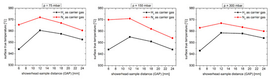
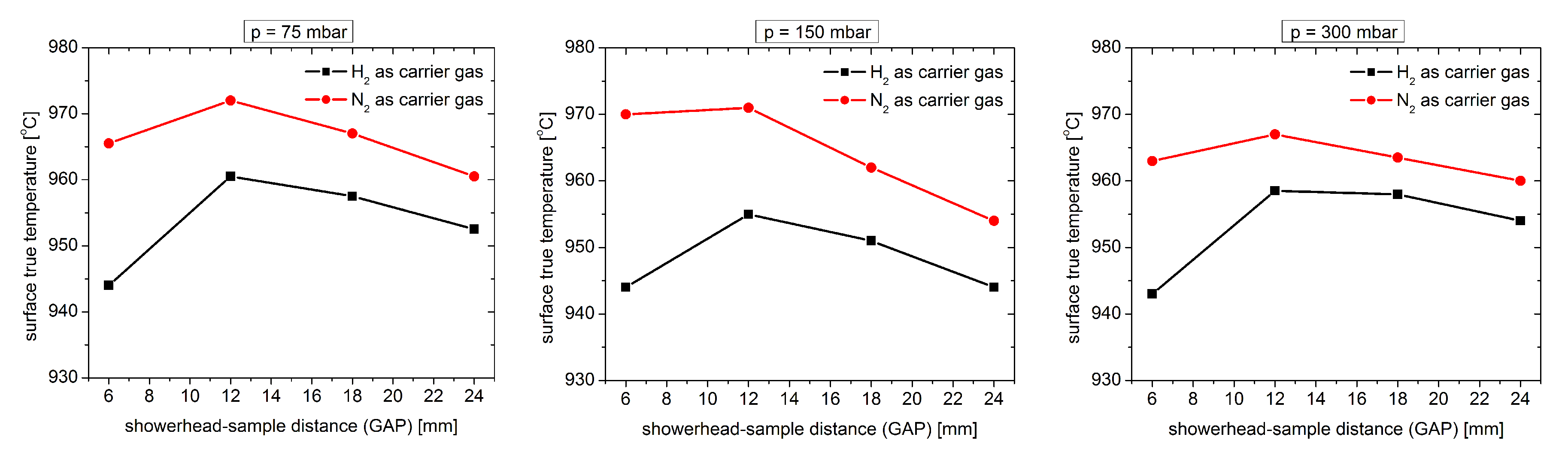
One of the main effects of changing the GAP distance is the modification of the real surface temperature of the substrate. Figure 1 shows how this value changes for different carrier gases (H and N) for a fixed thermocouple value (1140 C).
Figure 1.
Surface temperature as a showerhead-sample distance (GAP) function for a fixed thermocouple value (1140 C) for different pressures inside the reactor.
Real surface temperature was determined using the Laytec EPI TT system [6]. As can be seen, the real surface temperature of the substrate in the H atmosphere is always lower than for the case than for N used as carrier gas and changes slightly throughout the whole GAP range regardless of the pressure inside the reactor. This is due to the difference in thermal conductivity between H and N.
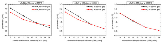
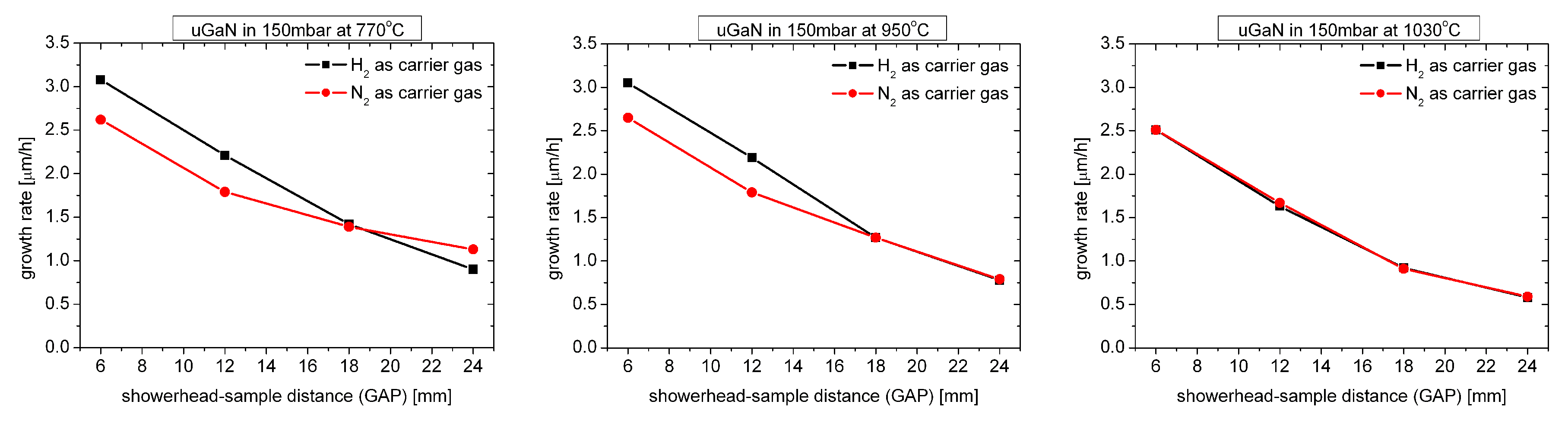
Figure 2 shows how the growth rate of undoped GaN layers (uGaN) grown at 150 mbar changes for three different growth temperatures.
Figure 2.
Growth rate of uGaN layers as a function of GAP distance for three different growth temperatures.
As can be seen, for high growth temperature (1030 C) the growth rate does not depend on the carrier gas used. For a typical growth temperature (950 C), it can be seen that for small GAP values (below 18 mm) the growth rate in H atmosphere is about 20% higher, what in the literature [7] is explained by the more effective decomposition of TMGa. For a low growth temperature (770 C) and the highest GAP value (24 mm), the growth rate in the N atmosphere is higher than in H, what is very unusual.
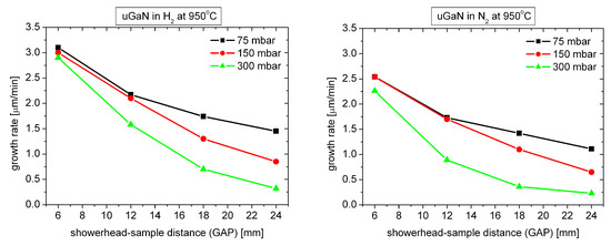
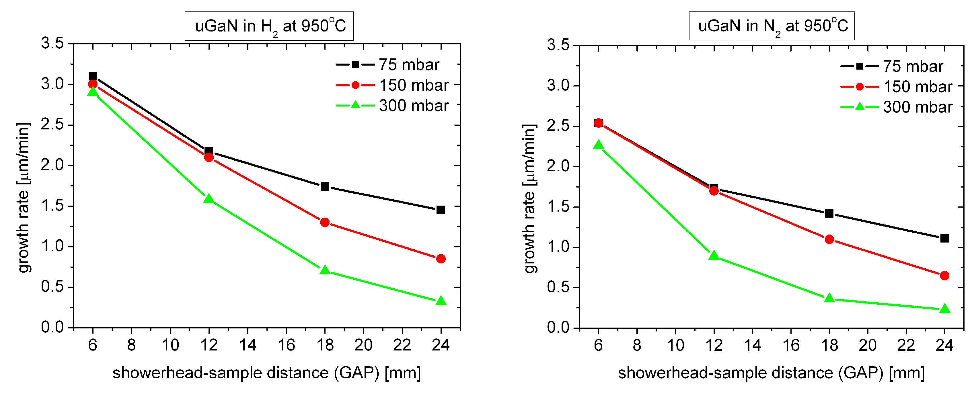
Figure 3 shows how the growth rate of undoped GaN layers (uGaN) grown at 950 C changes for three different growth pressures.
Figure 3.
Growth rate of uGaN layers as a function of GAP distance for three different growth pressures.
As you can see, regardless of the carrier gas used, the growth rate decreases significantly as the pressure in the reactor increases. The largest decrease is observed for the maximum GAP value. It should be assumed that increasing the pressure increases the thickness of the “boundary layer” between the gas phase and the solid state through which the reagents diffuse into the surface of the substrate [8].
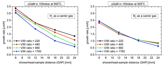
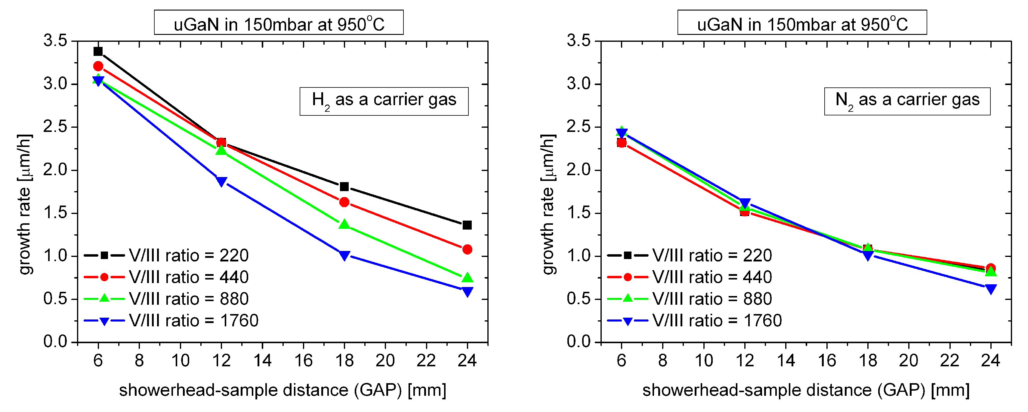
Another possible explanation of decreasing growth rate for high GAP value may be gas-phase parasitic reactions. Figure 4 shows how the growth rate changes in the GAP function for different V/III ratios changed by NH flow (at constant total flow).
Figure 4.
Growth rate of uGaN layers as a function of GAP distance for different V/III ratios (obtained for different NH flows).
As can be seen, when N is used as the carrier gas, the influence of NH flow is practically negligible. In case when H is used as a carrier gas, decreasing NH flow (lower V/III ratio) leads to an increase in growth rate, which can prove a smaller amount of parasitic reactions in the gas phase between NH and TMGa. Greater profit from reducing the amount of NH in the gas phase can be seen for higher GAP values.
4. Conclusions
We presented experimental results regarding GaN growth rate as a function of GAP for various temperatures, pressure, type of carrier gas and V/III ratio. In all cases, the increase of GAP resulted in a decrease of growth rate. The strongest effect of GAP value was at high pressure, what indicates gas phase parasitic reactions and, probably, because of the thicker/denser “boundary layer” above the substrate.
Author Contributions
Conceptualization, R.C. and M.L.; Methodology, R.C.; Validation, E.G. and M.L.; Formal Analysis, M.L.; Investigation, R.C.; Data Curation, R.C. and K.M. and W.O.; Writing—Original Draft Preparation, R.C.; Writing—Review & Editing, E.G. and M.L.; Visualization, R.C.; Supervision, M.L.; Project Administration, M.L.; Funding Acquisition, M.L.
Funding
This research was funded by National Centre for Research and Development grant in the frame of Polish-Chinese Cooperation number WPC/20/DefeGaN/2018.
Acknowledgments
The authors thank the Grant WPC/20/ DefeGaN/2018 of the National Centre for Research and Development.
Conflicts of Interest
The authors declare no conflict of interest.
References
- Aixtron. Available online: https://www.aixtron.com/en/products (accessed on 30 September 2019).
- Mrad, M.; Charles, M.; Mazel, Y.; Nolot, E.; Kanyandekwe, J.; Veillerot, M.; Ferret, P.; Feuillet, G. Understanding and controlling Ga contamination in InAlN barrier layers. J. Cryst. Growth 2019, 507, 139–142. [Google Scholar] [CrossRef] [Scilit]
- Zhou, K.; Ikeda, M.; Liu, J.; Zhang, S.; Li, Z.; Feng, M.; Tian, A.; Wen, P.; Li, D.; Zhang, L.; et al. Abnormal InGaN growth behavior in indium-desorption regime in metalorganic chemical vapor deposition. J. Cryst. Growth 2015, 409, 51–55. [Google Scholar] [CrossRef] [Scilit]
- Hiroki, M.; Oda, Y.; Watanabe, N.; Maeda, N.; Yokoyama, H.; Kumakura, K.; Yamamoto, H. Unintentional Ga incorporation in metalorganic vapor phase epitaxy of In-containing III-nitride semiconductors. J. Cryst. Growth 2013, 382, 36–40. [Google Scholar] [CrossRef] [Scilit]
- Zhu, J.; Fan, Y.; Zhang, H.; Lu, G.; Wang, H.; Zhao, D.; Jiang, D.; Liu, Z.; Zhang, S.; Chen, G.; et al. Contribution of GaN template to the unexpected Ga atoms incorporated into AlInN epilayers grown under an indium-very-rich condition by metalorganic chemical vapor deposition (MOCVD). J. Cryst. Growth 2012, 348, 25–30. [Google Scholar] [CrossRef] [Scilit]
- Laytec. Available online: https://www.laytec.de/epitt/ (accessed on 30 September 2019).
- Hardtdegen, H.; Hollfelder, M.; Meyer, R.; Carius, R.; Munder, H.; Frohnhoff, S.; Szynka, D.; Luth, H. MOVPE growth of GaAs using a N2 carrier. J. Cryst. Growth 1992, 124, 420–426. [Google Scholar] [CrossRef] [Scilit]
- Stringfellow, G.B. Organometallic Vapor-Phase Epitaxy: Theory and Practice; Elsevier Science: Amsterdam, The Netherlands, 2012. [Google Scholar]
© 2019 by the authors. Licensee MDPI, Basel, Switzerland. This article is an open access article distributed under the terms and conditions of the Creative Commons Attribution (CC BY) license (http://creativecommons.org/licenses/by/4.0/).