Abstract
Nuclear fusion experiments are becoming one of the most interesting focuses of research, given the hope of generating programmable, safe, and green energy. Among them, ASDEX (axially symmetric divertor experiment) upgrade has been operating at the Max Planck Institute for Plasma Physics (IPP) research center since 1991. To ignite and confine the plasma, several coils must be supplied through controllable high-current pulsed power supplies. The toroidal field magnets are here considered and a modular multilevel converter (MMC)-like system was designed and tested thanks to a small-scale prototype in previous works. The MMC-like topology, consisting of full-bridge submodules (SMs) with IGBTs and supercapacitor and exploitable also for other industrial applications, was chosen because of its modularity, redundancy, fault tolerance, and large amount of stored energy. The prototype, made of four SMs, was necessary to highlight critical key points in the design process. However, its scalability must be further tested before building a full-scale power supply, meant to reach almost 2400 SMs to guarantee the energy required by the load. This paper aims at validating hardware-in-the-loop (a powerful, safe, and relatively inexpensive real-time simulation environment that enables testing with real control boards) as a useful technology for power supply scalability studies and not only for control strategy tests. The results obtained previously from the prototype will allow us to finally increase the number of SMs and test the MMC-like scalability.
1. Introduction
The modular multilevel converter (MMC) has received considerable attention since the beginning of this century, and it has recently become one of the most attractive converter topologies for high-power and high-voltage applications [1,2,3]. MMCs have significant advantages compared with two-level converters, such as a scalable output voltage, distributed stored energy, and the option to easily replace failed submodules (SMs) in cases of fault [4]. On the other hand, the simultaneous control of a huge number of semiconductor switches remains one of the main challenges. The most common MMC topology for three-phase systems consists of six arms, each of which contains a series connection of n SMs and an arm inductor (Larm). Figure 1 shows a schematic of a three-phase MMC with one of the conventional SM configurations: full-bridge (FB) SM [5], composed of four insulated-gate bipolar transistors (IGBTs) and an SM capacitor, mainly acting as an energy storage system. The SM capacitor voltage vc(t) is influenced by the phase current flowing through the three-phase load (U, V, W phases), and each SM output voltage (vSM) can be toggled between four states depending on the IGBTs ones: vC, −vC or 0 (vSM is 0 in two different states). Consequently, the series connection of n SMs per arm can be used as a discrete-leveled voltage source: when r cells out of n are in the ON state (with 0 ≤ r ≤ n), the U phase load voltage equals the sum of the r capacitor voltages, and the same applies to phases V and W.
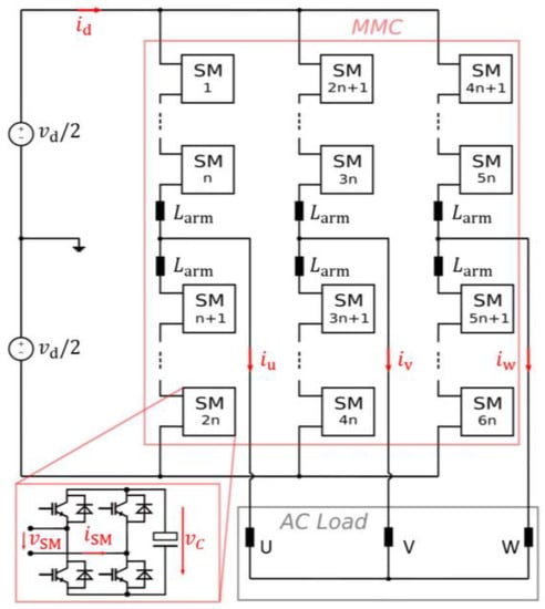
Figure 1.
Conventional MMC with SMs in full-bridge configuration [8].
The modularity, flexibility, fault tolerance, and redundancy of the MMC [6] have not gone unnoticed in the fusion world, where efficient high-power converters are becoming increasingly important to reduce the amount of power losses and to hopefully inject fusion-generated energy into the electrical grid in the future. A small-scale prototype of a revised version of the MMC has been built at the Max Planck Institute for Plasma Physics (IPP) in Garching (Germany), where ASDEX Upgrade (AUG)—the largest German tokamak—is operated. Due to its pulsed power requirement (tens of MW for each coil, reaching a total amount of GW power peaks in a few seconds for the whole system), the entire power supply (PS) system of AUG must be decoupled from the grid to avoid voltage and frequency-stability problems and is currently provided by three flywheel generators (FGs) [7]. The main concern about AUG’s present PS system is that, in the case of a permanent fault, there would be no available replacement for one or more of the three FGs. For this reason, a feasibility study of an MMC-like topology was designed to substitute the PS of the toroidal field (TF) coils and tested thanks to a small-scale prototype at IPP [8,9,10,11]. Being that the load of interest was a DC one (54 kA DC current and 2.6 kV peak voltage), the proposed converter, shown in Figure 2, is a one-phase MMC. In order to increase the energy that can be supplied to the load while decoupling it from the grid as desired, m SMs were connected in parallel (not only at the terminals of the load but also at each SM level) and the available stored energy of each SM was increased by replacing the capacitors with supercapacitors (SCs). This is not the first SC-based PS developed for fusion applications [12,13,14], but it is the first MMC-based one that has been studied to be scalable, fault-tolerant and suitable also for energy storages apart from fusion applications, such as 50 Hz grid stabilization purposes. Moreover, differently from conventional MMC, arm inductors, which are commonly used to control the currents of the MMC arms, are removed from the proposed topology to avoid very high voltage drops (proportional to the 54 kA DC current) and further bulkiness of these high-current PSs. Effective current sharing can be reached by designing the busbars with a specific impedance whose time constant matches the load one, as demonstrated in [11].
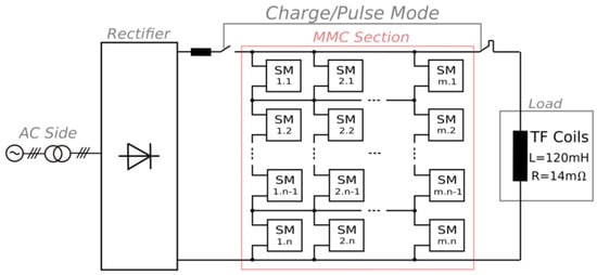
Figure 2.
Proposed MMC-based power supply for ASDEX Upgrade’s TF coils [8].
However, connecting several SMs both in series and in parallel is not a task that can be underestimated. In fact, a parallel operation that presents mismatches between the SMs state or voltage drops that differ among the m SMs can cause a wrong current sharing, which can consequently accelerate the aging of some components of the PS or possibly damage electronic devices [15,16,17,18]. On the other hand, the series operation can decrease the PS efficiency if proper voltage balancing is not performed [19,20,21,22]. The IPP small-scale prototype, made of four SMs, was strictly necessary to highlight critical key points in the series and parallel operations that must be considered during the design process in order to avoid the problems just mentioned [11]. However, its scalability must be further tested before building the full-scale PS meant to reach almost 2400 SMs to guarantee the energy required by the load. Due to the costs of prototypes, in terms of broken hardware and increased development times, quite significant and expensive high-power systems, this paper aims at validating the hardware-in-the-loop (HIL) methodology, a powerful, safe, flexible and relatively inexpensive real-time simulation environment that enables testing with real control boards. If the results obtained with the HIL test facility can match the measurements of a small-scale prototype comparing different test benches (Prototype, Simulation, and HIL) that all implement the same control strategy, the PS scalability tests could be performed through HIL before designing the PS with increased size. Hence, the goal is to validate the HIL as useful future technology to reduce time and costs by anticipating the issues related to the design, control and realization of a large-scale modular converter with increased size. In particular, modular converters can suffer significant synchronization issues amongst the submodules, which is a critical point not commonly discussed in the literature.
In order to present the results needed to validate the HIL technology for scalability tests, this paper illustrates an overview of the proposed converter and of the developed control strategy in the next two sections, while the fourth section describes the exploited hardware. Finally, the obtained results are discussed and conclusions are drawn.
2. MMC-like Converter: Main Design Choices
The converter can be described as an n × m matrix of SMs, where n and m are the number of modules in series and in parallel, respectively. In particular, the converter can be subdivided in m “arms” and n “rows”. SMs were initially intended to be half-bridge type—which would be theoretically sufficient for DC loads—but in order to increase the flexibility of the topology and make it suitable for AC loads, the FB SM configuration has been chosen. This choice is optimal also in terms of reliability: in the case of any SM internal fault (e.g., fault of one IGBT), it can still be bypassed thanks to the other available half-bridge without affecting the operation of the whole converter, which would not be possible with the half-bridge configuration. In this way, the converter can safely operate and the failed SM can be replaced directly after the operation.
The main objective of the converter is to generate a constant output current of 54 kA for about 10 s every 15–20 min. The SC modules are charged at their nominal voltage with a low charging current within this time interval, after which the matrix is ready for the next pulse. During a pulse, the duration of ramp-up and ramp-down phases is limited to reduce losses by applying all the available voltage (about 3 kV when SCs are charged) and the resultant dynamic is mainly affected by the inductive behavior of the load (Ll = 120 mH, Rl = 14 mΩ, 5·τl = 5 Ll/Rl = 42.86 s). During the 10 s of the flat-top phase, the current ripple must not exceed the 0.1% of its nominal value [8]. This value directly depends on the voltage difference (Δv) among the converter’s output voltage (vout) and load-resistive voltage drop vcu, on the load inductance Ll (whose voltage drop is defined as vL), and on the switching frequency fsw of the converter. SMs belonging to the same rows are synchronized in order to simplify the control strategy (see next sections) and they have the same output voltage, and thus vout can be expressed as:
where vSMj are n SMs voltages, Sj are the SMs states (which can be 1, 0 or –1 with the FB configuration) and vSCj are the n SC voltages. The current ripple can be therefore estimated as:
Since Ll is constant and Δv depends on the SC modules’ voltage, the current ripple can be reduced by increasing the switching frequency of the converter. Considering the maximum Δv as a worst case during the first milliseconds of the flat top (during the operation it decreases due to the discharge of the supercapacitors), an output switching frequency of 50 Hz would ensure the current ripple did not exceed 50 A. The inductive energy stored into the TF coils during the pulse can be recovered by the SC modules thanks to the four-quadrant operation of the FB SM.
A preliminary estimation of the total amount of SMs required to fulfill the TF coil requirements in terms of energy, voltage and current leads to about 1500 SMs needed. However, for this calculation, circuit losses have been neglected and it cannot be considered realistic. Only after having designed roughly the main components (SM SC module, power stage filter, etc.) could a second estimation be made including all relevant losses, leading to about 2400 total modules required (n = 25, m = 96).
3. Control Strategy
In order to simplify the control strategy and to decrease its implementation complexity, which is strictly necessary when considering the 2400 SMs of the full-scale power supply, it was chosen to control synchronously and equally the m SMs of each row. In fact, if SM synchronization were really reached, each row would behave coherently, reducing the risk of IGBT states and voltage mismatches, and consequently of faster component aging due to the existence of unbalanced SM currents and SC voltages. To achieve this goal, a specific communication protocol was chosen—EtherCAT [23,24]. This protocol computes the delay between the received signals of the first and last SM of each row and imposes a waiting time on each SM equal to the calculated delay in order to obtain a synchronized control implementation, except for small random delays in the order of tens of nanoseconds. Its accuracy is assured by the use of the distributed clocks method [24]. The physical circuit used to implement the EtherCAT communication protocol for the small-scale prototype is presented in [9,11] and in the next sections.
The choice of controlling synchronously and equally the m parallel-connected SMs of each row means that only one control signal must be generated by the control strategy per row. Its management and its implementation will be handled by the EtherCAT communication protocol and by the software and hardware configuration. Consequently, the n × m matrix can be modeled as a variable voltage source with 2n + 1 possible levels, as in Figure 3, where the minimum voltage step equals the voltage of one SC (vSC). These 2n + 1 voltage levels can be reached thanks to the four different states that each FB SM can assume:
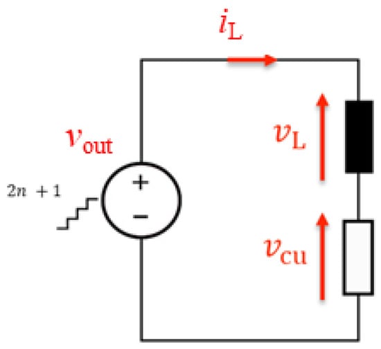
Figure 3.
Equivalent model of n × m matrix MMC-like converter if each row of m SMs is synchronized.
- SM enabled in direct mode (vSM = vSC);
- SM enabled in reverse mode (vSM = −vSC);
- SM by-passed (vSM = 0);
- Freewheeling mode.
Hence, the analyzed control strategy consists of two sections (one load current closed control loop and one voltage-balancing procedure) as shown in Figure 4 in order to fulfil the two main goals:
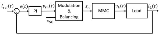
Figure 4.
Simplified block schema of the control strategy [11].
- Obtaining a load current ripple lower than 0.1% of nominal current value, which means lower than 54 A for TF AUG application.
- Discharge the SCs evenly to better exploit their available stored energy.
Load Current Tracking and SC Voltage Balancing
The two control sections are deeply explained in [10] and are here summarized for clarity. The first control loop is based on a closed loop current control: the load current iL(t) is measured and compared with a reference current iref(t), generating an error e(t). The error is then used as input for the main proportional integral (PI) controller, which provides to the inner control loop a normalized reference voltage vrn(t). It can be expressed as , where vr(t) is the reference output voltage of the converter and vsc(t) is the SC modules voltage measured in real time. The PI parameters were firstly tuned neglecting the inner balancing procedure and in continuous-time domain using Laplace transfer functions. It was considered an n × 1 MMC-like matrix system, exploiting the synchronization of the m parallel-connected SMs, together with the electrical parameters of the load (Rl, Ll) and of the cables (Rc, Lc) that connect the SMs. Hence, the proportional (kp) and integral (ki) parameters of the PI regulator have been defined by imposing the phase margin () and the cutoff frequency () in the open (Lm) and closed loop (Km) transfer functions:
resulting in:
All positive values of kp and ki were acceptable after applying the Routh–Hurwitz criterion to ensure the system’s asymptotical stability. Afterwards, the PI regulator was discretized by the Tustin transform in order for its implementation on a digital controller (also in simulations and not only in prototype and HIL experimental setup). Taking into account the filter design sized in [9] for the final AUG application, this paper keeps the same switching frequency (fsw = 50 Hz). For the full-scale power supply, such a low fsw allows EtherCAT to manage the total calculated row delay, dependent on the high number of parallel-connected SMs (m = 96) and consequent command latency [25], without exceeding the switching period, and while keeping the load current ripple below the desired limit as previously explained (iref − iL < 54 A). In fact, EtherCAT computes the latency of each of the n logical lines/rows constituted by m nodes and imposes a waiting time on each SM equal to the SM delay to guarantee row synchronization. However, the limitation to a maximum of n = 4 in the prototype or n = 8 in the HIL test bench means analyzing the SMs’ behavior to the detriment of the final load current ripple.
Focusing on the second control section, the signal vrn(t) is then used as input by the modulation and balancing control block of Figure 4. This subsystem firstly rounds the signal vrn(t) to the closest integer value in order to define the number of voltage levels required (modulation), and then it enables the needed number of SMs, which are chosen considering their respective SC module voltages (balancing). According to the real-time measurements of iL(t) and vsc(t), a sorting algorithm arranges the SMs in ascending/descending order depending on the iL(t) sign and on the rounded vrn(t): in this way, the first r SMs of the sorted list are selected to be enabled. On top of this, power stage error signals are also checked to detect potential short circuits in the test bench (also overheating in the case of the prototype). Therefore, the modulation and balancing control procedure generates n output signals forwarded to each row (composed by m parallel and synchronized SMs) depending on the desired SM state (bypassed, freewheeling, direct or reverse mode).
4. Control Strategy Implementation and Test Bench
In order to validate the HIL technology, the described control strategy has been tested by implementing the same EtherCAT communication system on the same control boards and by then interfacing this system with both HIL and prototype test benches. The main components are shown in the schema of Figure 5. They can be briefly described as follows (further details to understand their benefits and limitation in next sections).
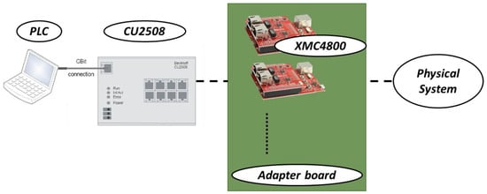
Figure 5.
Connection schema of PLC, EtherCAT communication system and HIL interface.
- PLC (Programmable Logic Controller): the host PC is converted into a PLC thanks to the software TwinCAT, which manages the control computations/execution, the EtherCAT protocol and the input/output (I/O) management. The I/O are, respectively, measurements from the control boards and control signals to the IGBTs [26].
- CU2508 Port Multiplier: it connects up to eight Ethernet networks and interfaces the PLC with the control boards by implementing the EtherCAT communication protocol and consequently the distributed clock method [27].
- Infineon XMC4800 Relax EtherCAT Kit with XMC EtherCAT PHY Board: relatively low-cost control board with EtherCAT communication protocol kit ready to use.
- Adapter board: hardware interface between control boards and physical system. It adapts the signal levels, both in voltage and in current, and connects the I/Os.
- Physical system: system to be tested, such as the proposed MMC-like topology, that can be real-time simulated in the case of HIL or real in the case of a prototype.
4.1. TwinCAT Implementation
The operations for the real-time control of the prototype have been performed by a PC, acting as a PLC though the TwinCAT software. The software handles communications with the microcontrollers, reading their inputs and controlling their output. The program implemented is organized as multiple nested loops, which are executed every certain number of cycles depending on the frequency required by different operations. A simplified scheme of the program is presented in Figure 6.
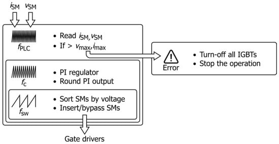
Figure 6.
Simplified scheme of the program implemented in TwinCAT.
The operations executed in every control cycle, thus at a frequency , are:
- reading all the values measured by the current, voltage and temperature sensors and read by the microcontrollers;
- checking if the read values are within the set limit, in case all the IGBTs will be commanded to be turned off and the operation will be stopped.
The calculations for the PI regulation are carried out at a frequency , lower than , and thus the inner loop is executed once every cycles.
The last inner loop is performed every cycles, and its operations are:
- sorting all SMs by their SC voltage;
- sending the commands to insert or bypass each SM depending on the balancing.
4.2. Control Board
The Infineon XMC4800 Relax EtherCAT kit with XMC EtherCAT PHY board, shown in Figure 7, is among the simplest and cheapest products supported by EtherCAT [28]: the top layer manages the EtherCAT protocol, while the bottom layer constitutes the main control board thanks to the microprocessor and ADCs. Each control board can read up to 6 measurements and can send up to 6 PWM signals. However, the vendor itself suggests not using 2 of the 6 available ADCs for this purpose, if possible. The ADC input voltage range (0 ÷ 3.3 V) is the most limiting factor when using this control board for high-power application. In fact, it means that the measurement range, from its minimum to its maximum value, must be scaled in 3.3 V, negatively affecting the signal-to-noise ratio. If we think to the final AUG’s application, for example, each SM should supply Iref/m = 54 kA/96 = 562.5 A, and taking some margins both in the maximum current that should be read (580 A) and in the maximum ADC voltage that should be reached (3 V), 1 A is read as ≈5 mV, which can be easily mistaken for noise, thus reducing the control performances. Considering that the prototype is based on FB SM and that the control strategy inputs are SC voltage vsc(t) and the load current computed as sum of the output current iSM(t) of m parallel-connected SMs, each SM requires 2 ADC and 4 PWM for control purposes. Hence, each control board is dedicated to one SM, and the other ADC signals can be used to monitor such data as IGBT temperature and SC current. Moreover, the additional PWM signals can be used as digital I/O to open/close relay or switches.
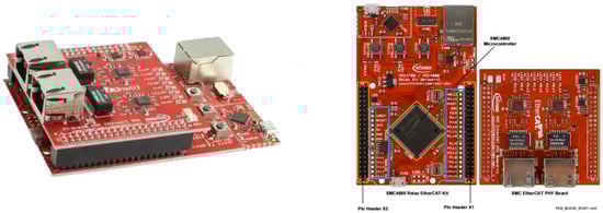
Figure 7.
Infineon XMC4800 Relax EtherCAT kit with XMC EtherCAT PHY board.
4.3. Prototype
A small-scale prototype (see Figure 8) has been developed to test the components of a single SM and test 4 SMs in series, parallel and mixed operation. Each SM is composed of a SC module, a power stage filter and two IGBT half-bridge modules. The SMs are controlled by their local microcontrollers, mounted on a custom board which—apart from adapting the microcontroller output signals—is also used as a diagnostics interface. This means that all the measurements signals (current, voltage, temperature and error signals) are adapted for the Infineon board ADCs. Details about the specific components of the prototype are provided in [9,11]. As already mentioned, the 4 SMs can be connected in series, parallel or combined series–parallel connections depending on the purpose of the experiment. Hence, the different configurations, which highlighted critical key points that must be considered during the design process, should be realized by connecting the busbars in a proper way to the respective output terminals of the SM. The busbars have been designed with a specific impedance whose time constant matches that of the load used for the parallel configuration experiments to avoid wrong current sharing [11]. The series configuration is realized by connecting the SMs via cables, since in this case the impedance between the SMs does not play any relevant role as long as it is negligible in comparison to the load impedance. The small-scale load impedance is characterized by Ll = 5 mH, Rl = 25 mΩ so as to achieve a load time constant tens of times lower than that of AUG (5·τl = 1 s instead of 5·τl = 42.86 s).
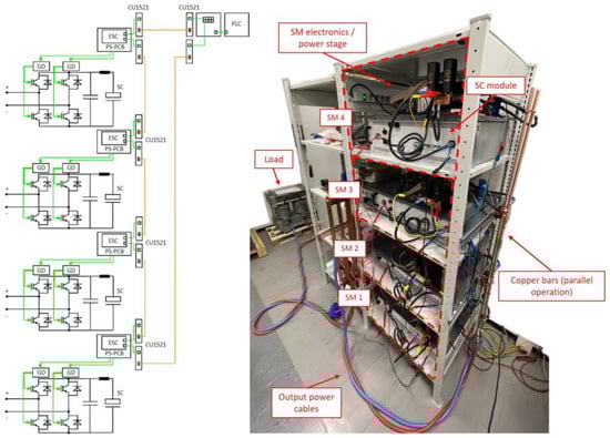
Figure 8.
Prototype schema (left) and experimental setup (right).
4.4. Hardware-in-the-Loop
The HIL platform available in our laboratory is a National Instruments (NI) HIL structure constituted by a PXIe-1071 chassis with PXIe-8840 CPU and PXIe-7868R FPGA module. The software implementation is performed through the LabVIEW FPGA environment and the Opal-RT eHS-64 solver, which is able to solve system equations in up to 72 states (switches + capacitors + inductors) in 1 µs. Hence, it can theoretically replace the prototype for testing control strategies and implementation without dealing with the prototype issues, such as safety, limited flexibility or costs. The presented hardware is constituted by 18 analogue output (AO) and 48 digital input output (DIO) channels. The AOs are characterized by a voltage range of ±10 V. Moreover, the NI hardware is flexible: additional modules can be connected to the chassis (e.g., to further investigate PS scalability), or it can work as a data acquisition system if different modules are connected to the same chassis.
As done for the prototype in [9], once the requirements of the Infineon control board, the NI HIL, and the application under analysis are clarified, the project of a board able to interface the two subsystems is executed. To take full advantage of the HIL possibilities and to test the MMC-like topology scaling, the maximum number of Infineon boards that can be interfaced to the HIL has been chosen. Hence, the adapter board has been realized in order to: connect 8 Infineon boards; read at least 2 AOs from the HIL per board; send at least 4 PWMs per board to the HIL; and adapt each signal between Infineon board and HIL. Moreover, the HIL Opal-RT eHS-64 solver limits are also taken into consideration: analyzing a maximum of 8 FB SMs means including 67 states (total number of switches, capacitances and inductances) in the constant admittance matrix used to solve the electrical circuit exploiting the Pejović method [29]. The resulting computation time step with 67 states is lower than 1 µs as declared by Opal-RT, which is fully compatible with the proposed control strategy implementation (chosen discretization time Ts = 2 ms). If the cable inductances Lc were also added, the solver would slow down without significant problems for this application.
Figure 9 shows from left to right the NI HIL, custom adapter board, eight Infineon control boards (four at the top and four at the bottom of the adapter board—only four of them are used for the 2 × 2 configuration) and one port multiplier that manages the synchronization of the parallel-connected SMs.
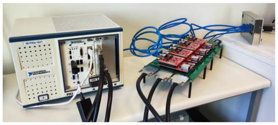
Figure 9.
HIL test facility.
5. Results
This section illustrates the results obtained with different test benches (Prototype, Simulation and HIL) that all implement the same control strategy. A specific MMC-like configuration (2 × 2 operation) is selected for the comparison, whose goal is to understand if the results obtained with the HIL test facility can easily match the measurements of a small-scale prototype. If true, future PS scalability tests could be performed through HIL before designing a PS of increased size. The peculiarities of the HIL methodology with respect to classical computer simulations are here highlighted.
5.1. 2 × 2 MMC-like: Comparison of Test Benches (Prototype vs. Simulation vs. HIL)
The four SMs that compose the Prototype test bench of Figure 8 allow us to test all the possible configurations of the proposed MMC-like topology (e.g., two series-connected and two parallel-connected SMs or four series-connected/parallel-connected SMs). However, only the 2 × 2 configuration, shown in Figure 10, has been investigated in this paper, as it was considered the option that best fits the scope of coil power supply. In fact, such a configuration, in comparison to the n × 1 case, has the following benefits. It doubles the available energy, allowing higher load currents for longer time intervals and halves the maximum available load voltage with respect to the 4 × 1 configuration, but it still validates the SC voltage balancing control.
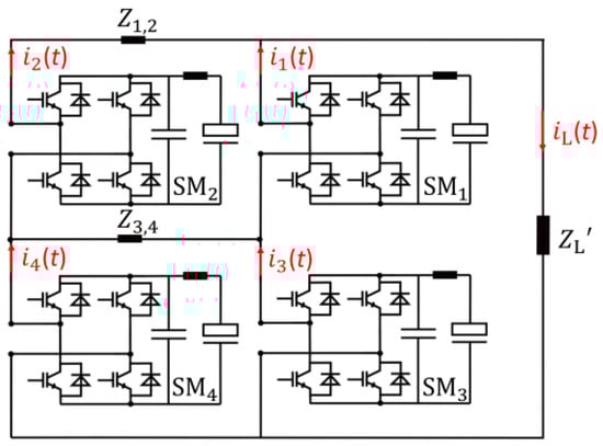
Figure 10.
Combined 2 × 2 series/parallel configuration schema [11].
Considering the control goals, a load current tracking a step reference of 600 A that lasts for 1 s is evaluated together with the SC voltage balancing in Figure 11. The load current is able to follow the reference profile (respectively, red and blue lines in Figure 11a), but having just n = 2 worsens the current ripple, as expected. In fact, it is limited (≈45 A) but higher than 0.1% of Iref (0.6 A). The current ramp-up and ramp-down phases are strictly related to the load time constant (5·τl = 1 s, if both SMs were included in the circuit until the end of the transient Il,ss = 2vsc/Rl = 1600 A). Figure 11b confirms both the control balancing effectiveness (the SC voltages of the two rows decrease coherently) and the disconnection of one of the two SMs at 2.1 s being iL > iref. These results are used as reference for the test benches’ comparison.
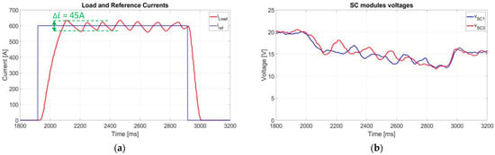
Figure 11.
2 × 2 Prototype setup results: (a) load (red) vs. reference (blue) current; (b) voltage on the SC (vsc1 = vsc2, vsc3 = vsc4) [11].
Starting with the Simulation environment, it is important to remember that even if it is one of the key tools for the power converter design (because of its inherent safety, flexibility and relatively low cost), each simulation increases its reliability and truthfulness only if the model complexity of the system increases too. Simulations that showed results compatible with the prototype ones were performed:
- Using a discretized solver with resolution time step (Tr = 1 µs) much lower than the control discretization time step (Ts = 2 ms) to correctly study the measurements’ waveform;
- Implementing a discretized control working at computational frequency fC = 1/Ts = 500 Hz and switching frequency fsw = 50 Hz;
- Including the measurement filtering action, implemented for the variables used to compute the control signals through moving average blocks;
- Choosing a suitable SM-equivalent model.
Different SM-equivalent models have been tested in the Plexim PLECS environment. Starting from the most detailed one of Figure 12 with the data of Table 1, thus including the parasitic elements of all circuit components, the most realistic case is evaluated. The strong similarities (ramp-up/down phase, load current ripple, SC voltage discharge and recovery) between the simulation results, shown in Figure 13, and of the prototype, in Figure 11, validate that a detailed simulation model can be a good method to approximate a real prototype. However, these results can be reached only after specific measurements on the prototype test bench, such as the ADC + sensors filtering action and the circuit parasitic elements.
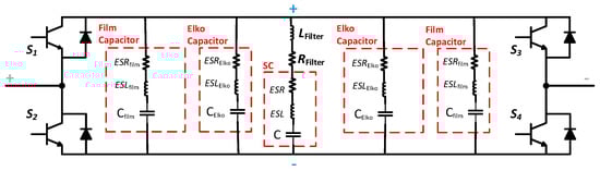
Figure 12.
FB SM composed of four IGBTs, SC and R-L-C filter with their parasitic equivalent series resistance and inductance (ESR and ESL, respectively).

Table 1.
SM main electrical parameters.
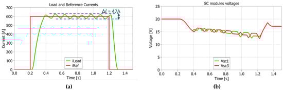
Figure 13.
2 × 2 Simulation results with detailed SM model: (a) load (green) vs. reference (red) current; (b) voltage of series-connected SCs (vsc1 = vsc2, vsc3 = vsc4).
The second test consisted in implementing the same control strategy (measurement filtering action included), but removing the parasitic terms of the filter from the SM, whose model is shown in Figure 14. Consequently, as it can be noticed in Figure 15, the load current ripple increases slightly (57 A instead of 47 A peak to peak) and the SC voltage recovery time constant changes in a negligible way, but the overall SC voltage and load current behavior is still close to Figure 11.
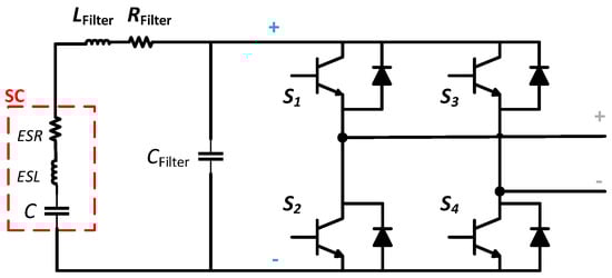
Figure 14.
FB SM composed of: four IGBTs, SC (C + ESR + ESL) and R-L-C filter without ESR and ESL.
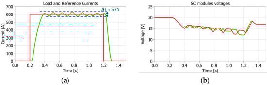
Figure 15.
2 × 2 Simulation results with SM model of Figure 14: (a) load (green) vs. reference (red) current; (b) voltage of series-connected SCs (vsc1 = vsc2, vsc3 = vsc4).
Completely different results are obtained if the SC ESR and ESL are removed from the SM model (see Figure 16) or if the measurement filtering action is excluded (see Figure 17). In the former, the load current ripple is almost twice the prototype one (110 A instead of 45 A peak to peak), and the load current tracking and the SC discharge are not coherent with Figure 11 in shape or absolute values. In the latter, the shape and the absolute values of both load current tracking and the SC discharge are again not relatable to those in Figure 11, but in a different way: the switching occurs more often, decreasing the load current ripple, and the balancing control effectiveness decreases because of voltage overshoots on the SC that are misinterpreted by the control system. However, while the SC ESR approximate value can be found on datasheets (ESL is lower than ESR and affects the results less), the control chain filtering action can hardly be evaluated without an existing prototype. This and other control implementation challenges, such as the resolution/limited input voltage of ADCs or the hardware/software management, are instead inherently addressed with an HIL test facility. In fact, the control board is really interfaced with a test bench through hardware components and not only modeled in a simulation environment.
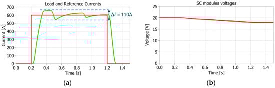
Figure 16.
2 × 2 Simulation results with SM model without parasitic terms: (a) load (green) vs. reference (red) current; (b) voltage of series-connected SCs (vsc1 = vsc2, vsc3 = vsc4).
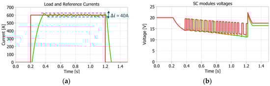
Figure 17.
2 × 2 Simulation results with SM model with SC parasitic terms without ADC filtering: (a) load (green) vs. reference (red) current; (b) voltage of series-connected SCs (vsc1 = vsc2, vsc3 = vsc4).
In the next step, the HIL results of Figure 18 are compared with the prototype ones of Figure 11. It can be noticed that the load current tracking conforms to expectations: ramp-up/down phase of 0.2 s and load current ripple of 42 A instead of 45 A peak to peak. The SC voltage discharge is also close to the prototype one (≈14 V instead of ≈13 V). What really changes is the SC voltage shape: the prototype one results in being more filtered because of sensor filtering in the control chain. Hence, part of the measurement filtering action is lost in these tests, but it could be included by implementing an average block that is proportional to sensor maximum frequency. This result is important to remember in that what is measured on a prototype with the sensors’ filtering action could differ from what really occurs in the circuit and what should be really measured, including strong and fast current/voltage peaks that could damage the physical system if they were not detected. On the other hand, problems such as signal-to-noise ratio of ADCs and the hardware/software management (including real-time data communication and PWM synchronization mismatch) are inherently addressed with the HIL test facility, whereas the latter cannot be even partially evaluated in a simulation environment. It follows that the HIL can be reasonably taken into consideration to allow the designers of power converters, in particular for the complex topologies needed for high-power PS, to develop, test and debug control algorithms and to scale modular converters, avoiding risks of breaking physical systems, which are particularly significant in terms of broken hardware and increased development times.
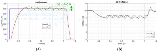
Figure 18.
2 × 2 HIL setup results: (a) load (red) vs. reference (blue) current; (b) voltage of series-connected SCs (vsc1 = vsc2, vsc3 = vsc4).
5.2. MMC-like Scalability: HIL vs. Detailed Simulation Model Results
Since the goal is to find a relatively cheap, but reliable, method to scale up the prototype in the future, the following points should be considered based on the results obtained in the previous paragraph:
- Directly increasing the size of the prototype would be expensive and not completely flexible to the testing needs;
- Only the results obtained with the detailed simulation model and the HIL test facility are comparable with the prototype ones;
- The detailed simulation model can only achieve good results after specific measurements on the prototype test bench. Therefore, it is not effective if different components are to be tested.
Hence, the detailed simulation model is used to validate the HIL as a useful methodology for scaling up modular converter topologies and to show the results that the full-scale converter is expected to reach if designed with the aforementioned hardware.
In particular, considering the demanding requirements on load current ripple and on flat-top phase duration (10 s for AUG, but hundreds of seconds for future fusion experiments as Divertor Tokamak Test facility [14,30]), two cases have been analyzed: a 4 × 2 and a 2 × 4 configuration. The former aims at validating the benefits and limitations of configurations where the series-connected SMs are the majority (n > m), while the latter, on the contrary, studies the configurations where n < m.
As seen from the results analyzed in the previous section, the detailed simulation model performed in PLECS fits the prototype results better because the same filtering action of the sensors is included in the control chain, whereas the HIL results lose part of the measurement filtering action, but are more compliant with what should be currently measured in the circuit. Hence, HIL current and voltage measurements are expected to have similar dynamics for the former, which is strongly limited by the inductive load behavior (5·τl = 1 s), and faster dynamics for the latter, respectively, in comparison to PLECS results.
Firstly, the number of series-connected SMs (n) is increased considering the 4 × 2 configuration. Figure 19 and Figure 20 show the PLECS and HIL results, respectively. From the configuration point of view, increasing n while slightly decreasing the SMs’ initial voltage (17 V instead of 20 V) allows us to obtain a higher-performance load current tracking (error equal to 37 ÷ 38 A instead of 45 A) with the same step reference of 600 A that lasts for 1 s, as in Figure 11. The most critical point for the case n > m is the limited amount of stored energy and consequently of flat-top phase duration. Furthermore, although the number of SMs to be managed has increased, the correct functioning of the voltage balancing control is again demonstrated. Instead, from a comparison point of view, the expectations on the dynamics of the HIL measurements when compared to the PLECS results are proven here by obtaining similar load current transients (same ramp-up/down phase and similar ripples of 38 A instead of 37 A peak-to-peak), but different SC voltage discharge characteristics: same final value ≈12 V, but different time constant and final recovery overshoot (≈14 V in PLECS but ≈17 V in HIL).
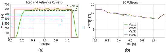
Figure 19.
4 × 2 Simulation results with detailed SM model: (a) load (green) vs. reference (red) current; (b) SC voltages: 1st number = row, 2nd number = arm.
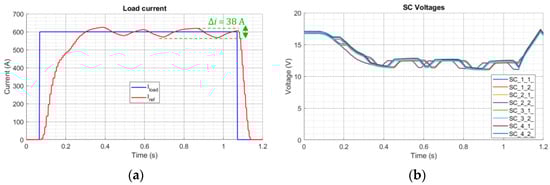
Figure 20.
4 × 2 HIL setup results: (a) load (red) vs. reference (blue) current; (b) SC voltages: 1st number = row, 2nd number = arm.
On the other hand, Figure 21 and Figure 22 (respectively, PLECS and HIL results) show the validity of the proposed MMC-like topology when increasing m. In fact, just doubling the number of parallel-connected SMs allows the duration of the current reference to be at least tripled. As the final voltage is close to 14 V, the experiment could be further extended without losing the effectiveness of the load current tracking or of the voltage balancing control, which are again verified by obtaining a load current ripple equal to 41 ÷ 44 A and a consistent balanced reduction of SC voltages. Again, from a comparison point of view, previous statements about HIL dynamics are here confirmed through similar load current transients and different SC voltage discharge characteristics: same final value ≈ 14 V, but different time constant and final recovery overshoot (≈15 V in PLECS, but ≈17 V in HIL).
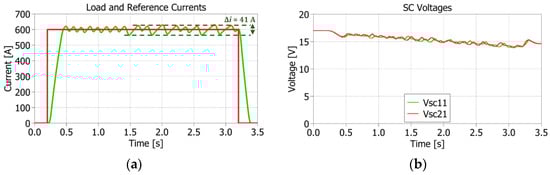
Figure 21.
2 × 4 Simulation results with detailed SM model: (a) load (green) vs. reference (red) current; (b) SC voltages: 1st number = row, 2nd number = arm.
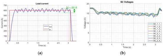
Figure 22.
2 × 4 HIL setup results: (a) load (red) vs. reference (blue) current; (b) SC voltages: 1st number = row, 2nd number = arm.
Finally, in order to foresee the results of the full-scale PS and the effectiveness of the proposed control strategy, a simulation with a detailed model is performed, taking advantage of the synchronization provided by EtherCAT. Thus, the 25 × 96 MMC-like converter is simulated by considering 25 × 1 SMs, where each SM includes the stored energy and the losses of 96 SMs connected in parallel, to decrease the simulation computational burden. The current scenario of the TF coil for the final AUG’s application is here taken into account. Thus, a step reference of Iref = 54 kA that lasts for 12 s is imposed. Figure 23 shows the load current profile with respect to Iref and the resultant tracking error. After a first ramp-up phase, whose dynamics are strongly limited by the load inductive behavior as in the final ramp-down phase (if vsc = constant and all the SMs supply energy to the load, steady-state is reached in 42.86 s at Iss = 162 kA), the flat-top phase starts. Figure 23b highlights that the main control goal is fully achieved even if a very low switching frequency is used (fsw = 50 Hz), since the load current peak-to-peak ripple is limited to 25 A, lower than the imposed maximum ripple of 54 A. On the other hand, Figure 24 shows the voltage measured at the SC terminals. Given that the detailed simulation model of Figure 12 is considered, the voltage used as input of the control includes the voltage drops due to the SC parasitic elements (ESR and ESL), but the overshoots due to the ESL are smoother than the ones that would occur in reality, thanks to the implemented ADC + sensors filtering action that emulates what the control board would read. The balancing control procedure is effective, since the SC voltages evenly discharge and the final partial charge of the SC is due to the recovery of the energy stored in the TF coil.
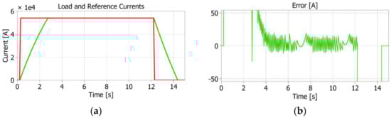
Figure 23.
25 × 96 Simulation results with detailed SM model: (a) load (green) vs. reference (red) current; (b) error between measured and reference currents in [A].
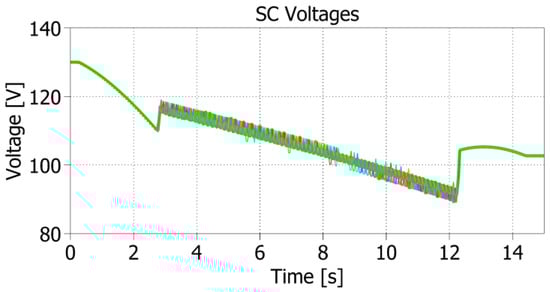
Figure 24.
25 × 96 Simulation results with detailed SM model: SC voltages.
6. Conclusions
This paper has provided the outcomes from applying the HIL methodology on a specific hardware configuration to validate it as a useful instrument for power-supply scalability tests. A modular multilevel converter (MMC)-like topology, consisting of full-bridge supercapacitor submodules (SMs) and exploitable for high-power industrial applications, was chosen because of its modularity, redundancy, fault tolerance and large energy storage capability. Such a configuration was already under study and under test at the Max Planck Institut for Plasma Physics (IPP, in Garching, Germany) to supply toroidal field coils (54 kA DC current and 2.6 kV peak voltage).
Following an initial explanation of the converter topology and the related control strategy, a detailed description of the HIL test facility was presented to subsequently understand the validity of the results. The laboratory setup includes the same control boards exploited in the small-scale prototype, the available NI HIL running an OPAL-RT solver and a custom adapter board designed for this specific application.
A comparison of the results obtained by testing the prototype, the simulation and the HIL environments has been performed. The simulation environment (usually preferable because of its inherent safety, flexibility and relatively low cost) can reach a good approximation of the prototype data only after increasing the model complexity and including specific evaluations of the prototype test bench, such as the ADC + sensor filtering action and the circuit parasitic elements. Reducing the complexity of the model leads to inaccurate results. Furthermore, the control code needed for the specific microcontroller implementation cannot be tested. On the other hand, the HIL environment inherently addresses problems that cannot be even partially evaluated in a simulation environment, such as hardware/software management (including real-time data communication and PWM synchronization mismatch). The results from the HIL matched the ones from the prototype, with an exception made for the absence of a sensor filtering action, which could be easily included by implementing an average block that is proportional to the sensor maximum frequency.
Even if the detailed simulation model can only achieve good results after specific measurements on the prototype test bench and is not effective if changes occur in components, it was useful to validate the HIL as a methodology for scaling up modular converter topologies by obtaining a consistent comparison between their results with a 2 × 4 and a 4 × 2 configuration. Hence, the HIL can be taken into consideration not only to allow the designers of power converters, in particular for the complex topologies needed for nuclear fusion power supplies, to develop, test and debug control algorithms, but also to scale modular converters, avoiding risks of breaking physical systems, which are particularly expensive in high-power systems, as the costs of prototypes in terms of broken hardware and increased development times are quite significant.
Finally, in order to foresee the results of the full-scale converter (25 × 96), a simulation with a detailed model is performed confirming the general effectiveness of the MMC-like topology design and of the implemented control strategy, reaching a maximum load current ripple (≈25 A) lower than the limit imposed by AUG (54 A), while evenly discharging the SMs.
Author Contributions
Conceptualization, C.T. and A.M.; methodology, C.T.; software, C.T., A.M. and F.S.; validation, C.T.; investigation, C.T.; resources, C.T., A.M. and S.B.; writing—original draft preparation, C.T., A.M. and F.S.; writing—review and editing, C.T., A.M., F.S. and S.B.; visualization, C.T.; supervision, S.B. All authors have read and agreed to the published version of the manuscript.
Funding
This work has been carried out within the framework of the EUROfusion Consortium, funded by the European Union via the Euratom Research and Training Programme (grant agreement 101052200—EUROfusion). The views and opinions expressed are those of the author(s) only and do not necessarily reflect those of the European Union or the European Commission. Neither the European Union nor the European Commission can be held responsible for them.
Data Availability Statement
The data presented in this study are available on request from the corresponding author.
Conflicts of Interest
The authors declare no conflict of interest.
References
- Dekka, A.; Wu, B.; Fuentes, R.L.; Perez, M.; Zargari, N.R. Evolution of Topologies, Modeling, Control Schemes, and Applications of Modular Multilevel Converters. IEEE J. Emerg. Sel. Top. Power Electron. 2017, 5, 1631–1656. [Google Scholar] [CrossRef]
- Rodriguez, J.; Franquelo, L.G.; Kouro, S.; Leon, J.I.; Portillo, R.C.; Prats, M.M.; Perez, M.A. Multilevel Converters: An Enabling Technology for High-Power Applications. Proc. IEEE 2009, 97, 1786–1817. [Google Scholar] [CrossRef]
- Abu-Rub, H.; Holtz, J.; Rodriguez, J.; Baoming, G. Medium-Voltage Multilevel Converters—State of the Art, Challenges, and Requirements in Industrial Applications. IEEE Trans. Ind. Electron. 2010, 57, 2581–2596. [Google Scholar] [CrossRef]
- Martinez-Rodrigo, F.; Ramirez, D.; Rey-Boue, A.B.; De Pablo, S.; Herrero-de Lucas, L.C. Modular Multilevel Converters: Control and Applications. Energies 2017, 10, 1709. [Google Scholar] [CrossRef]
- Deng, F.; Lü, Y.; Liu, C.; Heng, Q.; Yu, Q.; Zhao, J. Overview on submodule topologies, modeling, modulation, control schemes, fault diagnosis, and tolerant control strategies of modular multilevel converters. Chin. J. Electr. Eng. 2020, 6, 1–21. [Google Scholar] [CrossRef]
- Rohner, S.; Bernet, S.; Hiller, M.; Sommer, R. Modulation, Losses, and Semiconductor Requirements of Modular Multilevel Converters. IEEE Trans. Ind. Electron. 2009, 57, 2633–2642. [Google Scholar] [CrossRef]
- Käsemann, C.; Grois, E.; Stobbe, F.; Rott, M.; Klaster, K. Pulsed power supply system of the ASDEX upgrade Tokamak research facility. In Proceedings of the IEEE 15th International Conference on Environment and Electrical Engineering (EEEIC), Rome, Italy, 10–13 June 2015; pp. 237–242. [Google Scholar]
- Magnanimo, A.; Teschke, M.; Griepentrog, G. Supercapacitors-based power supply for ASDEX upgrade toroidal field coils. Fusion Eng. Des. 2021, 171, 112574. [Google Scholar] [CrossRef]
- Magnanimo, A.; Teschke, M.; Griepentrog, G. Full-Bridge Submodule Development of an MMC-Like Topology for ASDEX Upgrade Toroidal Field Coils Power Supply. IEEE Trans. Plasma Sci. 2022, 50, 2178–2184. [Google Scholar] [CrossRef]
- Terlizzi, C.; Berardi, D.; Santoro, F.; Magnanimo, A.; Teschke, M.; Bifaretti, S. Voltage balancing algorithm of a MMC-like topology for pulsed power applications. In Proceedings of the 2022 AEIT International Annual Conference (AEIT), Rome, Italy, 3–5 October 2022; pp. 1–6. [Google Scholar]
- Magnanimo, A.; Griepentrog, G.; Santoro, F.; Terlizzi, C.; Teschke, M. Development of a MMC demonstrator for nuclear fusion devices power supplies. Fusion Eng. Des. 2023, 188, 113433. [Google Scholar] [CrossRef]
- Maffia, G.; Lampasi, A.; Zito, P. A new generation of pulsed power supplies for experimental physics based on supercapacitors. In Proceedings of the IEEE 15th International Conference on Environment and Electrical Engineering (EEEIC), Rome, Italy, 10–13 June 2015; pp. 1067–1072. [Google Scholar]
- Lampasi, A.; Taddia, G.; Tenconi, S.M.; Gherdovich, F. Compact Power Supply with Integrated Energy Storage and Recovery Capabilities for Arbitrary Currents up to 2 kA. IEEE Trans. Plasma Sci. 2018, 46, 3393–3400. [Google Scholar] [CrossRef]
- Lampasi, A.; Romano, R.; Cocchi, A.; Zito, P. Poloidal Power Supply System of the Divertor Tokamak Test (DTT) Facility. In Proceedings of the 2020 IEEE 20th Mediterranean Electrotechnical Conference (MELECON), Palermo, Italy, 16–18 June 2020; pp. 634–639. [Google Scholar]
- Akagi, H. What Led to Success in Academic Research on the Family of Modular Multilevel Cascade Converters? In Proceedings of the 2018 International Power Electronics Conference (IPEC-Niigata 2018-ECCE Asia), Niigata, Japan, 20–24 May 2018; pp. 2352–2359. [Google Scholar]
- Santoro, F.; Ferro, A.; De Nardi, M.; Gaio, E. Studies on Alternative Schemes for the MMC-Based Acceleration Grid Power Supply of DEMO Neutral Beam Injector. IEEE Trans. Plasma Sci. 2022, 50, 4039–4046. [Google Scholar] [CrossRef]
- Tu, Q.; Xu, Z.; Xu, L. Reduced Switching-Frequency Modulation and Circulating Current Suppression for Modular Multilevel Converters. IEEE Trans. Power Deliv. 2011, 26, 2009–2017. [Google Scholar] [CrossRef]
- Fang, J.; Blaabjerg, F.; Liu, S.; Goetz, S.M. A Review of Multilevel Converters with Parallel Connectivity. IEEE Trans. Power Electron. 2021, 36, 12468–12489. [Google Scholar] [CrossRef]
- Sharifabadi, K.; Harnefors, L.; Nee, H.-P.; Norrga, S.; Teodorescu, R. Design, Control and Application of Modular Multilevel Converters for HVDC Transmission Systems; John Wiley & Sons Inc.: New York, NY, USA, 2016. [Google Scholar]
- Debnath, S.; Qin, J.; Bahrani, B.; Saeedifard, M.; Barbosa, P. Operation, Control, and Applications of the Modular Multilevel Converter: A Review. IEEE Trans. Power Electron. 2014, 30, 37–53. [Google Scholar] [CrossRef]
- Marzo, I.; Sanchez-Ruiz, A.; Barrena, J.A.; Abad, G.; Muguruza, I. Power Balancing in Cascaded H-Bridge and Modular Multilevel Converters Under Unbalanced Operation: A Review. IEEE Access 2021, 9, 110525–110543. [Google Scholar] [CrossRef]
- Marquardt, R. Modular Multilevel Converters: State of the Art and Future Progress. IEEE Power Electron. Mag. 2018, 5, 24–31. [Google Scholar] [CrossRef]
- Nguyen, V.Q.; Jeon, J.W. EtherCAT network latency analysis. In Proceedings of the 2016 International Conference on Computing, Communication and Automation (ICCCA), Greater Noida, India, 29–30 April 2016; pp. 432–436. [Google Scholar]
- Cena, G.; Bertolotti, I.C.; Scanzio, S.; Valenzano, A.; Zunino, C. Evaluation of EtherCAT Distributed Clock Performance. IEEE Trans. Ind. Inform. 2011, 8, 20–29. [Google Scholar] [CrossRef]
- Correa, T.P.; Almeida, L. DiSortNet: A Network Protocol with Distributed Sorting for Modular Multilevel Converters. IEEE Open J. Ind. Electron. Soc. 2022, 3, 223–235. [Google Scholar] [CrossRef]
- EtherCAT: PLC and Motion Control Software TwinCAT. Available online: https://www.ethercat.org/en/products/EE89D3E40659427C8D3458706B14AC57.htm (accessed on 24 February 2023).
- BECKHOFF: CU2508. Available online: https://www.beckhoff.com/it-it/products/i-o/infrastructure-components/cuxxxx-ethernet-port-multiplier/cu2508.html (accessed on 24 February 2023).
- EtherCAT: Product Guide. Available online: https://www.ethercat.org/en/products.html (accessed on 7 March 2023).
- Pejovic, P.; Maksimovic, D. A method for fast time-domain simulation of networks with switches. IEEE Trans. Power Electron. 1994, 9, 449–456. [Google Scholar] [CrossRef]
- Terlizzi, C.; Bifaretti, S.; Lampasi, A. Current Sharing Control Strategy for parallel-connected H-Bridges DC-DC Converter: Modelling, Analysis and HIL test. In Proceedings of the 2021 IEEE Energy Conversion Congress and Exposition (ECCE), Vancouver, BC, Canada, 10–14 October 2021; pp. 2777–2783. [Google Scholar]
Disclaimer/Publisher’s Note: The statements, opinions and data contained in all publications are solely those of the individual author(s) and contributor(s) and not of MDPI and/or the editor(s). MDPI and/or the editor(s) disclaim responsibility for any injury to people or property resulting from any ideas, methods, instructions or products referred to in the content. |
© 2023 by the authors. Licensee MDPI, Basel, Switzerland. This article is an open access article distributed under the terms and conditions of the Creative Commons Attribution (CC BY) license (https://creativecommons.org/licenses/by/4.0/).