Article

A Bridge-Level Junction Temperature Estimation Method for SiC MOSFETs Combining Transient Voltage and Current Peaks

State Key Laboratory of Power Transmission Equipment and System Security and New Technology, Chongqing University, Chongqing 400044, China
*
Author to whom correspondence should be addressed.
Energies 2023, 16(10), 4105; https://doi.org/10.3390/en16104105
Submission received: 18 April 2023 / Revised: 10 May 2023 / Accepted: 11 May 2023 / Published: 15 May 2023

Abstract

:
Accurate measurement of the junction temperature Tj is crucial for ensuring safe operation and evaluating the performance of silicon carbide (SiC) metal–oxide–semiconductor field-effect transistors (MOSFETs). In this paper, the junction temperature of a half-bridge is monitored by combining transient voltage and current peaks across the lower device. Both theoretical analysis and switch tests validate that the peak induced voltage and peak reversed current during the commutation transient exhibit a linear relationship with the temperature of the corresponding devices. The impact of load current and bus voltage on the measurement results is also investigated. Moreover, the effectiveness of the proposed method is confirmed by carrying out tests at different temperatures, and the feasibility of online implementation is discussed. The experimental results show that the proposed method has high linearity and sensitivity and can simultaneously provide temperature information for both devices of a half-bridge.

1. Introduction

The silicon carbide metal–oxide–semiconductor field-effect transistor (SiC MOSFET), as a typical representative of wide-bandgap semiconductor devices, has superior properties, such as high switching frequency, high voltage withstanding capability, and low on-resistance. With the widespread application of silicon carbide devices in fields such as rail transportation, aviation and aerospace, automotive, and new energy generation in recent years [1,2], the requirements for their reliability are increasing. Temperature is one of the main causes of power device failure [3], so temperature measurement is of great significance for the safe and reliable operation and thermal management of power electronic devices [4,5].
At present, temperature measurement methods mainly comprise thermal network, physical contact, optical, and temperature-sensitive electrical parameter (TSEP). The accuracy of the thermal network method has been improved [6,7]; based on the power loss of the device under testing and the transient thermal impedance model, the junction temperature can be calculated. However, obtaining the real-time loss of SiC MOSFET can be challenging. Additionally, the thermal impedance network is subject to the effects of device aging and environmental factors, which can influence the accuracy of the calculated junction temperature. The physical contact and optical methods require the decapsulation of power devices, which reduces system reliability [8,9]. Conversely, the TSEP method is advantageous due to its low cost, fast response, and ability to measure junction temperature without causing damage to the package. It is currently the most widely used temperature measurement method.
The temperature-sensitive electrical parameters of SiC MOSFET devices can be categorized into static and dynamic parameters based on different measure timings. The static electrical parameters include internal gate resistance [10], on-state voltage drop [11], on-state resistance [12], and body diode voltage drop [13]. The sensitivity of the internal gate resistance is relatively low, making its measurement difficult. The on-state voltage drop shows a positive correlation with temperature under a high current, although it requires high-resolution voltage clamp circuits during switching transients. The voltage drop across the body diode is also sensitive to temperature changes and remains stable during device aging; however, online application of this parameter is challenging, since its measurement requires injecting a small current into the source-drain.
The dynamic temperature-sensitive electrical parameters consist of dynamic threshold voltage [14], turn on/off delay [15,16], and peak gate current, et cetera. A measurement scheme proposed in [16] enables online measurement of the device’s turn-on delay during inverter operation. However, the sensitivity is at the picosecond level, thus necessitating intelligent driving circuits for improved accuracy. Reference [17] obtains the gate peak current by measuring the voltage across the external drive resistor, which can be easily measured online and integrated, as it is not affected by the load current. Nonetheless, this method is not suitable for gate drive topologies with inductors or push–pull structure.
Regarding bridge-level TSEPs, reference [18] utilized the voltage oscillation on the DC bus caused by the current change rate to extract the temperature of the half-bridge. This method needs to combine the switching timing of the upper and lower switches and cannot simultaneously reflect the bridge temperature in one switching period. Furthermore, real-time digital acquisition of the transient process requires the use of high-precision ADC and signal-processing circuits.
In summary, the existing TSEP methods for SiC MOSFET devices have certain limitations, such as difficult measurement, low linearity, and low sensitivity. Furthermore, research on the dynamic TSEPs of SiC MOSFET devices has typically only focused on device-level parameters, instead of using bridge- or system-level parameters to estimate temperature. The conventional single-TSEP can be influenced by the temperature of other devices in practical applications [19]. Additionally, multiple floating grounds at bridge midpoints bring common mode interference issues [20], requiring additional isolation design of the measurement circuit to monitor the upper switch.
In contrast to traditional device-level TSEPs, this paper proposes a novel method for measuring junction temperature at the bridge level, using the transient reverse recovery current peak and the voltage peak induced by the current change rate as combined TSEPs. The proposed method overcomes the need for measurement circuits at floating grounds, as it only requires one measuring unit at the lower switch of the phase leg. Moreover, it can reflect the temperature of the phase leg simultaneously within one same switching period. The switching process of each SiC MOSFET device during the commutation stage is explained specifically, and the correlation between the proposed TSEPs and the corresponding device temperature is analyzed. Subsequently, a dynamic switching characteristics platform is established to calibrate the peak induced voltage and peak reverse recovery current at different temperatures. The effects of load current and bus voltage on the temperature calibration curve are also evaluated, and the online feasibility of the proposed method is discussed. This method utilizes the inherent parasitic inductance of the SiC MOSFET discrete device itself, without the need for external sensors, making it non-intrusive and suitable for bridge-level temperature estimation of the SiC MOSFET device.

2. Theoretical Analysis of Combining Transient Peaks as a Bridge-Level TSEP

2.1. Commutation Process of SiC MOSFETs in a Phase Leg Structure

The schematic diagram of the half-bridge test circuit considering parasitic parameters is shown in Figure 1a. S1 is the upper switch, which is actively controlled by a double-pulse drive to the gate, and S2 is the lower switch, with a constant negative bias on the gate to ensure the channel is completely turned off. The body diode of S2 is used to provide a freewheeling loop for the load current. The main parasitic parameters in the circuit include: external and internal gate resistance Rg, external and internal gate loop parasitic inductance Lg, drain-source parasitic inductance Ld, power source drain parasitic inductance Lsp, Kelvin source drain parasitic inductance Lsk, and the sum of the parasitic resistance in series between the power source drain and Kelvin source drain, Rs.
The main switch waveforms of S1 and S2 are shown in Figure 1b, and the specific commutation process analysis is as follows:
① (t0~t1): This stage is the delay period for S1 to turn on. The gate voltage vgs1 rises from the negative voltage VEE to the threshold voltage Vth with a time constant of Rg (Cgs + Cgd). During this stage, vgs1 < Vth, and the load current flows through the body diode of S2.
② (t1~t2): In this stage, the load current is commutated from the body diode of S2 to the channel of S1. After the gate voltage vgs1 rises to the threshold voltage Vth, the channel current id1 of S1 rises to the load current IL at a rate of did1/dt, and id2 decreases to zero at the same rate.
At this time, vds1 >> (VGGVth), S1 is in a saturation region, and the drain-source current id1 can be expressed as:
i d 1 = β 2 ( v gs 1 V th ) 2
β = W CH μ CH C OX L
where β is the gain coefficient, WCH is the channel width of the inversion layer, and μCH is the effective carrier mobility of the channel.
The current change rate during this commutation stage can be calculated as:
d i d 1 d t = β ( v gs 1 V th ) V GG R g ( C gs + C gd ) e t R g ( C gs + C gd )
③ (t2~t3): This stage is the charge storage stage. The current of S1 continues to rise from IL to IL + Irrm, while the current of S2 continues to decrease from zero to a negative value. During this process, the free carriers in the drift region are swept away. At t2, the free carriers are zero, and the depletion region begins to form. At t3, the reverse recovery current reaches the negative peak value Irrm.
The peak reverse recovery current has the following relationship with the distribution of free carrier concentration [21]:
I rrm = 2 q D a d n d x = 2 q D a n a h
where Da is the bipolar diffusion coefficient, q is electron charge, and h is defined as the distance between the maximum and minimum carrier concentrations.
The carrier concentration na can be expressed as:
n a = I L τ HL 2 q d
where τHL is the minority carrier lifetime, and d is half of the drift region width.
④ (t3~t4): This stage is the reverse recovery stage. S2 begins to withstand voltage, and at the same time, the parasitic capacitance of S1 begins to discharge, while the parasitic capacitance of S2 begins to charge. The current of S2 during this stage consists of two parts: the actual reverse recovery current caused by the formation of the depletion region and the current charging the parasitic capacitance.
⑤ (t4~t5): In this stage, the reverse recovery process of S2 ends, and S1 enters the linear ohmic region.

2.2. Temperature Dependence Analysis

2.2.1. Peak Induced Voltage

From Figure 1a, it is evident that there exist a parasitic inductance Lsk and a parasitic inductance Lsp between the power source s and the auxiliary source s’ of the discrete SiC MOSFET device with a Kelvin package. The induced voltage vss′ at the two source terminals can be utilized to reflect the current change rate did2/dt. In the commutation process as depicted in Figure 1b, the channel of S2 is completely turned off; the induced voltage vss′ is only influenced by the power loop and can be given by:
v ss = L sp ( d i d 2 d t ) + R s i d 2
As analyzed in Section 2.1, during t1 to t3, the current of S2 drops from the load current at a speed of did1/dt, and the induced voltage at this time can be further expressed as:
v ss = L sp ( d i d 1 d t ) + R s i d 2 ,   t 1 < t < t 3
Owing to the wide bandgap property of SiC MOSFET devices, did1/dt exhibits a positive temperature coefficient under the dominating influence of the device threshold voltage Vth [22].
The induced voltage peak Vss′max appears at the moment when the current change rate reaches its maximum value. From Equations (1) and (3), during t1 to t2, the drive voltage rises approximately linearly, and the drain-source current increases in a quadratic function form, indicating that the maximum current change rate occurs at t2. At this moment, the peak induced voltage can be expressed as:
V ss max = L sp ( d i d 1 d t ) max + R s i d 2
According to the device datasheet and manufacturer Spice model, the typical value of the source parasitic resistor Rs is usually in the range of 3 to 5 mΩ, while the parasitic inductance Lsp is about a few nH, and the switching current change rate of SiC MOSFET devices is around 0.5–3 A/ns. Therefore, vss′ is mainly composed of induced voltage drop caused by parasitic inductance, and the changes caused by the temperature drift of parasitic resistance Rs is negligible. Upon determining the internal factors, such as the doping process and the physical size of the device during manufacturing, the parasitic parameter Lsp can be considered a fixed value [14]. Thus, under the influence of the positive temperature characteristic of (did1/dt)max, Vss′max has a positive correlation with temperature and is only affected by the temperature of S1.

2.2.2. Peak Reverse Recovery Current

Based on Equations (4) and (5), it is apparent that the peak reverse recovery current of a SiC MOSFET device is affected by the minority carrier recombination rate in the drift region, which is closely related to the minority carrier lifetime τHL and the bipolar diffusion coefficient Da, with Da exhibiting a negative temperature coefficient [21]. Furthermore, the relationship between the minority carrier lifetime and temperature can be described mathematically, as given by Equation (9) [21]. The minority carrier lifetime in the drift region increases exponentially with temperature, causing an increase in Irrm. Thus, Irrm is affected by the temperature of S2.
τ H L = τ 0 ( T j 300 ) k
In the current commutation process, the body diode of S2 is turned off by active controlling of the complementary switch S1. When the external switch speed did1/dt is decreased, the gradient of the minority carrier concentration in the drift region is reduced, causing a decline in the peak reverse recovery current of the body diode. Additionally, did1/dt is also impacted by the temperature of the upper switch S1, as discussed in Section 2.2.1. Therefore, the temperature of S1 also has an impact on Irrm.
The positive peak voltage Vss′max and the negative peak current Irrm both occur at the same switching transient. While Vss′max is affected independently by the junction temperature of S1, Irrm is affected by the temperature of S1 and S2. Consequently, it is possible to establish the two electrical parameters as functions of Tj1 (junction temperature of S1) and Tj2 (junction temperature of S2), as shown in Equations (10) and (11), if the correlation is highly linear, which would be calibrated in later experiments.
V ss max = f v ss max ( T j 1 ) = a T j 1 + b
I rrm = g I rrm ( T j 1 , T j 2 ) = c T j 1 + d T j 2 + e
By carrying out offline calibration experiments under fixed operating voltage and current, and various junction temperatures, the values of Vss′max and Irrm can be determined. Subsequently, the functions of the two TSEPs with respect to device temperatures can be established using mathematical tools such as MATLAB. This approach offers a feasible solution for determining the temperature of devices in a phase leg configuration simultaneously, by only sampling the electrical parameters of the lower switch.

3. Experimental Results

3.1. Temperature Dependence

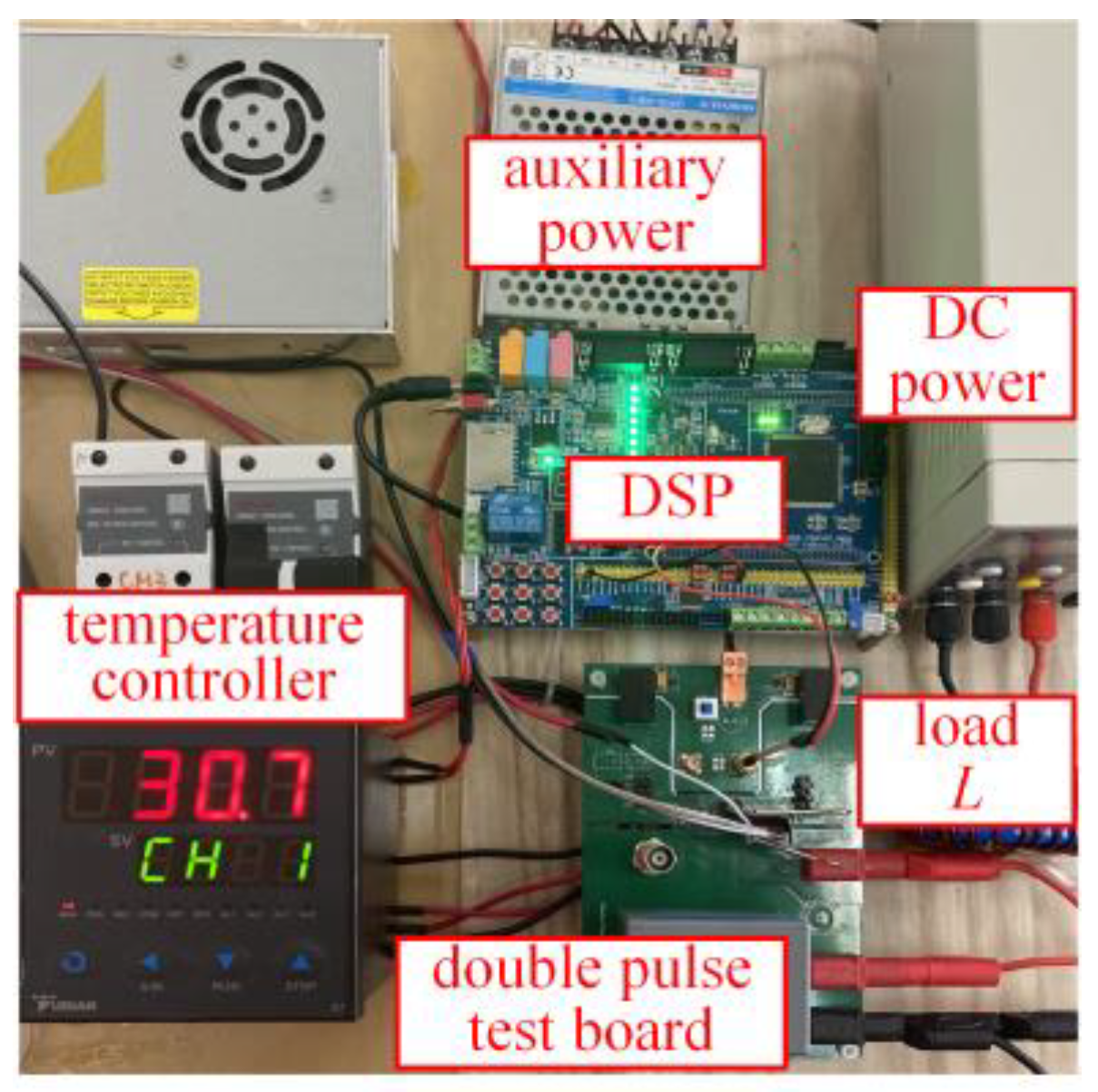
The double-pulse test platform shown in Figure 2 is built to verify the temperature characteristics of the proposed TSEPs. The test is performed under the operating conditions of a bus voltage of 300 V and a load current of 10 A, with both upper and lower switches in the phase leg being Wolfspeed’s discrete SiC MOSFET devices C2M0045170P (Wolfspeed, Durham, NC, USA), rated for a voltage and current level of 1700 V/72 A.
Due to the switching speed of SiC MOSFET devices being in the nanosecond range, high-bandwidth measuring equipment is required to ensure accurate measurements. Specifically, the bandwidth margin should be designed to be three to five times greater than the calculated value. According to signal theory, the effective bandwidth of the signal rise time tr or fall time tf should be [23]:
f BW = 0.35 min ( t r , t f )
For instance, as calculated by Formula (12), a 3dB bandwidth of at least 35 MHz is required to measure the turn-on current during a ten-nanosecond period. Considering a margin of five times, the measuring equipment should have a bandwidth of at least 175 MHz. Therefore, device voltage and current measurements in this paper are conducted using a 500 MHz passive voltage probe and a 1 GHz shunt resistor, respectively, and the oscilloscope used is Tektronix’s DPO7104C (Beaverton, OR, USA).
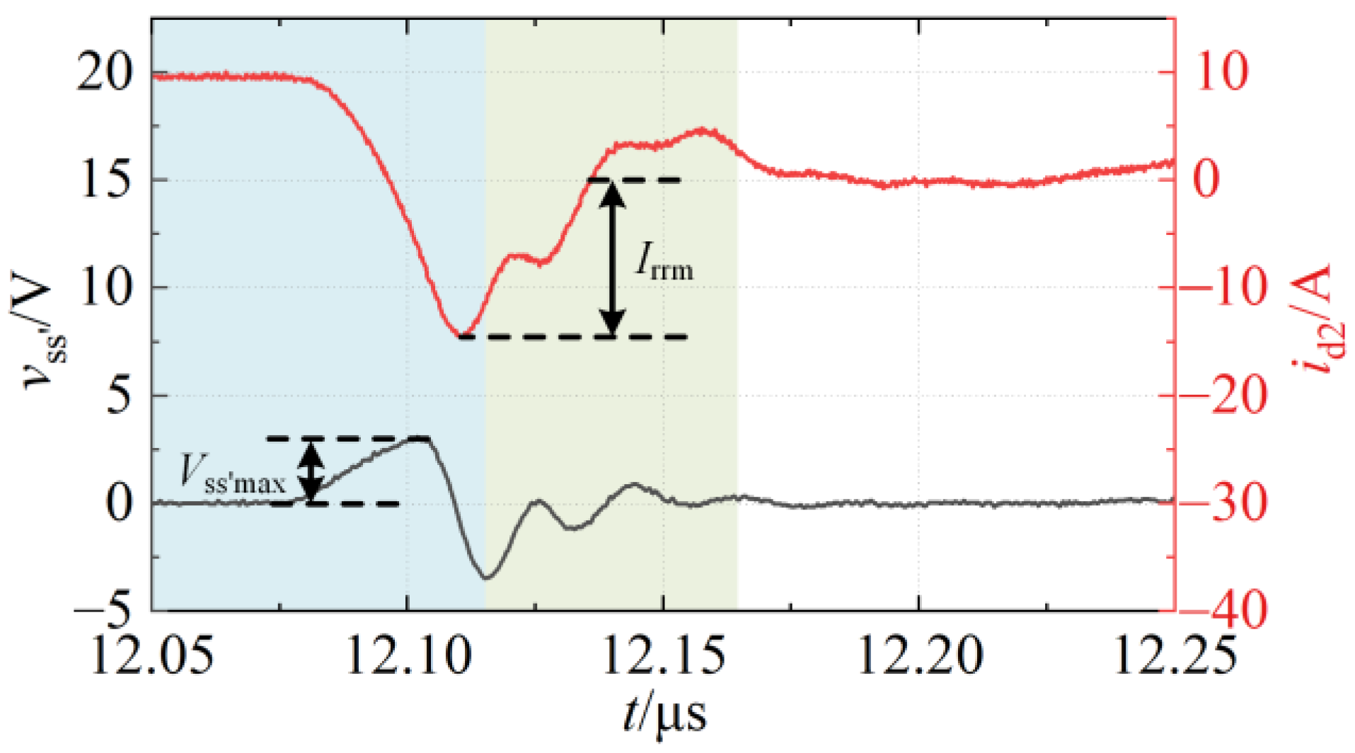
The transient experimental waveforms are illustrated in Figure 3. As the current change rate of id2 in the commutation process begins to drop, a voltage with a peak value of approximately 3 V is generated at the parasitic inductance Lsp of the lower switch. Considering the propagation delay of about three to five nanoseconds between the voltage waveform measured by the passive probe and the current waveform measured by the coaxial shunt resistor [24], the peak induced voltage appears around the moment when the load current crosses zero, which is the S2 temperature insensitive region, and is consistent with the theoretical analysis.
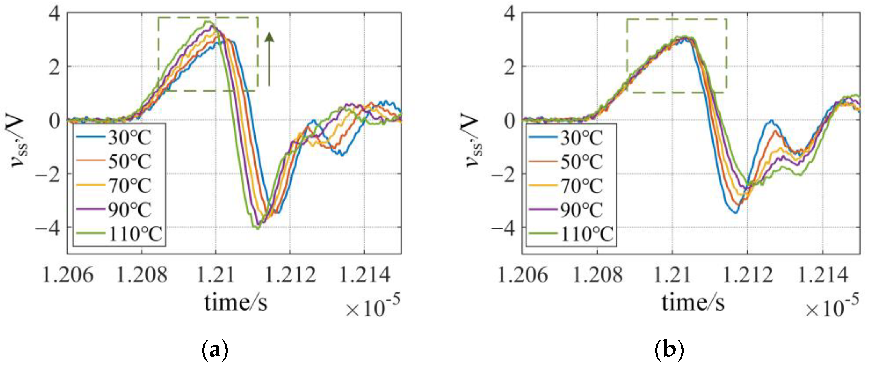
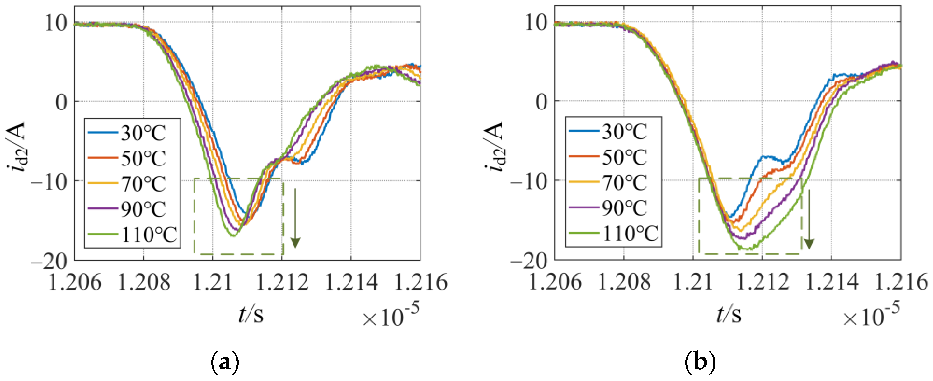
During the test, a PID temperature controller is utilized to control the device under testing. The temperature of the heating pad is set to 30 °C, 50 °C, 70 °C, 90 °C, 110 °C, and 130 °C to observe id2 and vss′ waveforms. Figure 4a displays the waveform when S1 is heated and S2 is maintained at room temperature. In contrast, Figure 4b shows the waveform with S2 heated and S1 at room temperature.
As illustrated in Figure 4, under the same operating conditions, Vss′max rises with the increasing temperature due to the positive correlation between (did1/dt)max and Tj1. The temperature change of Tj2 does not impact the current change rate before its body diode enters the reverse recovery process. Hence, Vss′max remains unaffected within the tested temperature range of S2. The experimental results align with the theoretical analysis.
The same testing approach is employed to capture id2 waveforms when the upper and lower switches operate at different temperatures, as shown in Figure 5. It is apparent that Irrm is dependent on both S1 and S2 and increases with the rising temperature, owing to the impact of the device carrier lifetime and the switch speed of the complementary device.

3.2. Operating Conditions Dependence

The relationship between Vss′max and Irrm, with junction temperature obtained under different load currents and a fixed bus voltage, is shown in Figure 6. The results demonstrate that both Vss′max and Irrm exhibit high temperature sensitivity at any load current. The increase in load current results in a greater number of free charge carriers in the drift region, leading to a larger reverse recovery process. Therefore, the temperature sensitivity of Irrm increases with increasing load current and is approximately −53 mA/°C, −62 mA/°C, and −86 mA/°C for load currents of 10 A, 15 A, and 20 A, respectively.
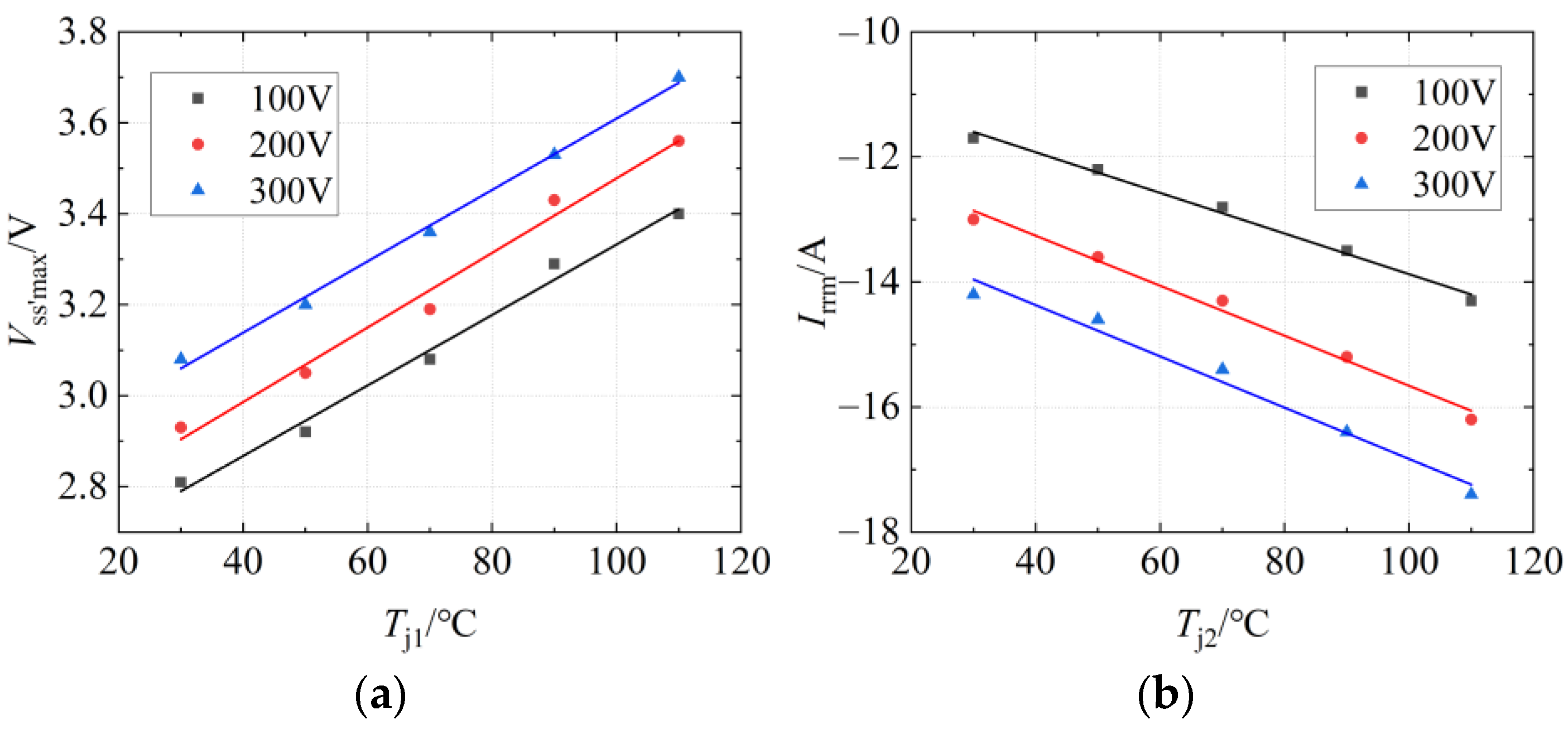
Figure 7 displays the relationship between Vss′max and Irrm with the junction temperature under different bus voltages. The depletion layer of the device widens with an increase in bus voltage, which decreases the depletion layer capacitance Cdep and accelerates the switching transient. Meanwhile, the device needs to produce a wider space charge region at higher bus voltages. The value of the combined TSEPs will thereby be affected by bus voltage. The fitted results in Figure 7 indicate that the temperature characteristic displays a similar trend under the tested bus voltage of 100 V, 200 V, and 300 V, and the absolute values of Vss′max and Irrm increase with an increase in bus voltage.
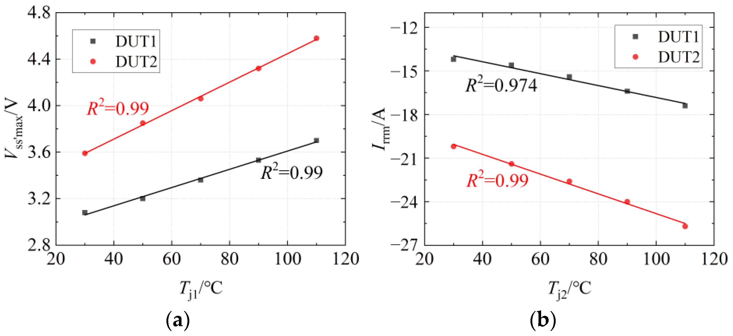
To validate the universality of the proposed method, a different discrete SiC MOSFET device C3M0030090K from Wolfspeed (Durham, NC, USA), rated at 900 V/73 A, is selected for the same experimental verification. The junction temperature calibration curves for the two different types of devices are shown in Figure 8. The experimental results demonstrate that the combined TSEPs exhibit a similar temperature variation trend for different devices.
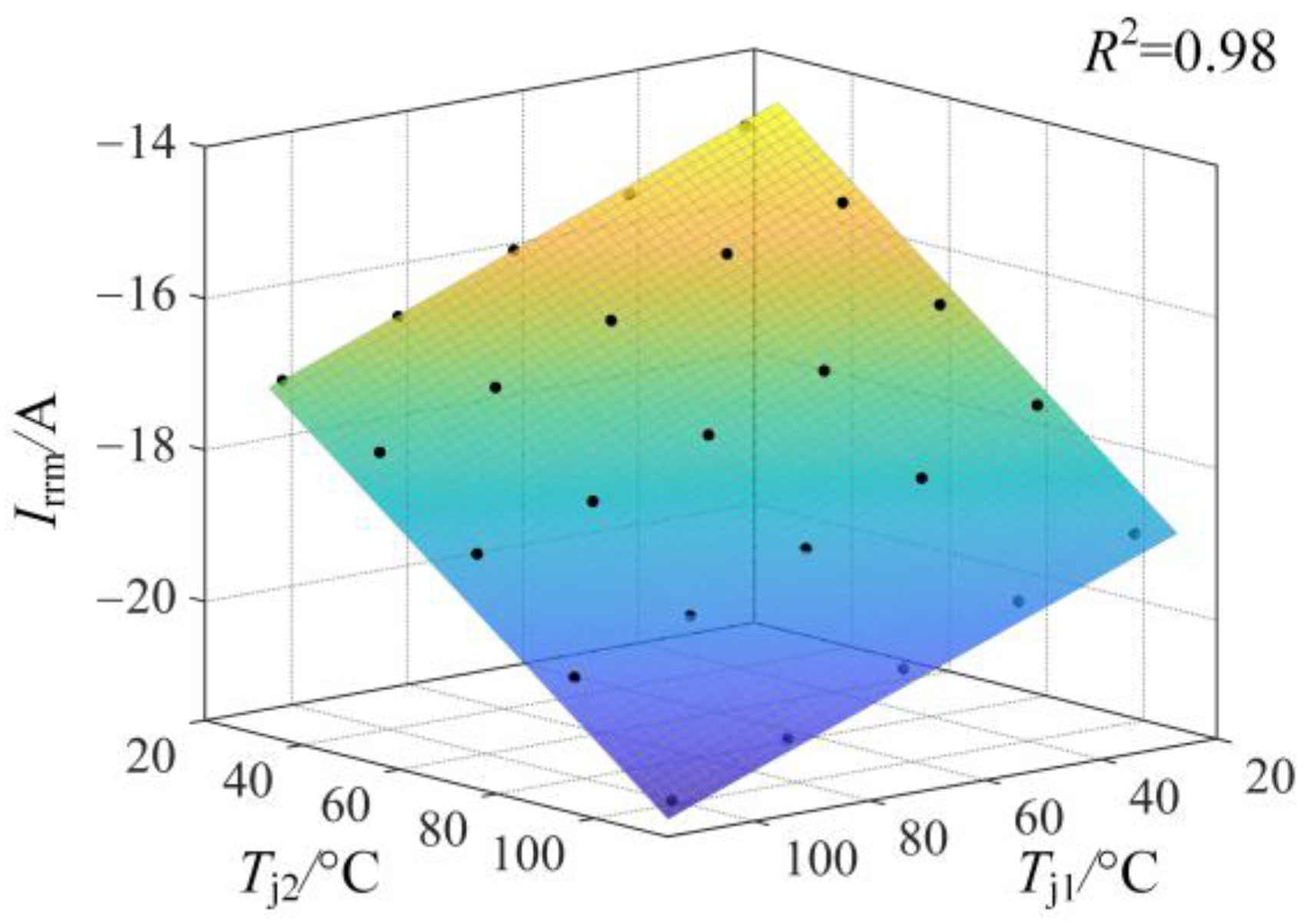
Based on the obtained experimental results, it can be observed that the device junction temperature Tj, peak induced voltage Vss′max, and peak reverse recovery current Irrm exhibit a nearly linear relationship, with a fitting coefficient R square over 0.97. Specifically, at a bus voltage of 300 V and a load current of 10 A, an increase of 1 °C in Tj1 leads to a rise of approximately 10 mV in Vss′max, while a temperature rise of 1 °C in Tj2 results in an absolute value increase of 44 mA in Irrm. The combined TSEPs demonstrate high sensitivity and linearity. In addition, since the sensitivity of Irrm increases with a larger load current, the accuracy of the proposed method will be further improved in higher current applications. The calibrated relationship between Irrm and the junction temperature of S1 and S2 is presented in Figure 9.
By substituting the experimental data into Equations (10) and (11) and employing MATLAB for linear fitting, the value of the coefficients a, b, c, d, and e can be mathematically obtained:
V ss max = f v ss max ( T j 1 ) = 0.007895 T j 1 + 2.822
I rrm = f I rrm ( T j 1 , T j 2 ) = 0.02895 T j 1 0.05317 T j 2 + 12.24594
The function between the phase leg temperature and the combined TSEPs under given working conditions can be derived as:
{ T j 1 = 126.6624 V ss max 357.4414 T j 2 = 68.9656 V ss max 18.8076 I rrm 35.6959
where in Equations (13)–(15), the units of voltages, currents, and temperatures are given in volts, amperes, and Celsius degrees, respectively.

4. Temperature Verification and Online Measurement Discussion

To validate the accuracy of the proposed method, experimental verification is conducted by heating both S1 and S2 to another temperature of 130 °C. At this time, the peak reverse recovery current and the peak induced voltage are 23 A and 3.85 V, respectively, as shown in Figure 10. The derived Equation (12) is then utilized to calculate the temperature of the upper and lower switches, which are found to be 130.2 °C and 131.4 °C, with an error of less than 1.5 °C.
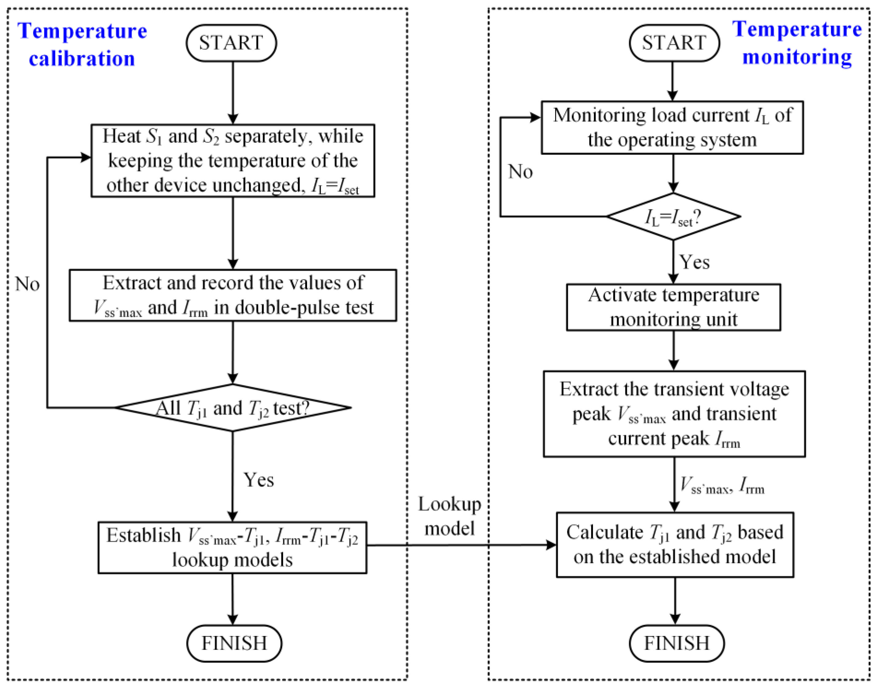
When the proposed method is applied to actual systems, offline calibration of the SiC MOSFET device is performed beforehand. According to the experimental results, the variation in bus voltage affects the combined TSEPs. Hence, the proposed method is best suited for applications where the bus voltage remains constant. When extracting the junction temperature in the actual converter, only the current sensor needs to capture the specific load current Iset to trigger the temperature monitoring unit. Subsequently, the measurement circuit can be employed to extract Vss′max and Irrm at the lower switch, and the bridge temperature could be obtained based on the established lookup model.
The peak induced voltage Vss′max can be directly obtained by using a peak detection circuit. Similarly, the peak reverse recovery current Irrm can be obtained by sampling vss′ and applying an integrator to the s and s’ lead [25]. The complete measurement flowchart is illustrated in Figure 11.
It is worth noting that both parameters, Vss′max and Irrm, can be obtained with the help of parasitic inductance. The accuracy of the method is solely dependent on the measurement accuracy of voltage Vss’ max and current Irrm. However, accurate determination of parasitic inductance can just as well avoid the repetitive offline calibration process for different devices in the same circuit, which can be realized by the methods suggested in [26,27]. As a result, the proposed method is non-intrusive and can ensure the normal operation of the system.
Device degradation is a common challenge for the majority of the existing TSEPs utilized for SiC MOSFETs [28]. Specifically, the reliability of gate oxide affects the peak induced voltage Vss′max, as bias temperature instability (BTI) stress can cause a shift in di/dt [29]. Additionally, device package degradation has an effect on both peak induced voltage Vss′max and peak reverse recovery current Irrm. To mitigate estimation errors resulting from device degradation, it is necessary to periodically recalibrate the TSEP of the SiC MOSFET with respect to temperature.

5. Conclusions

This paper proposes a novel bridge-level junction temperature measurement method for SiC MOSFETs by combining the transient voltage and current peaks across the lower switch. It is found that in a half-bridge commutation process, the peak induced voltage has a positive temperature coefficient with the upper switch, and the peak reverse recovery current has a positive temperature coefficient with both upper and lower devices.
A DPT platform is used for switching characteristic analysis. Both peak induced voltage Vss′max and peak reverse recovery current Irrm demonstrate a desirable linear relationship with temperature at a steady state. The temperature sensitivity of Vss′max to the upper switch is about 8 mV/°C, while that of Irrm to the lower switch is about −53 mA/°C when the bus voltage is 300 V and the load current is 10 A.
The accuracy of the proposed method is verified by testing at another temperature point through the DPT platform, where the bridge temperature can be independently monitored with an error margin of less than 1.5 °C. All the parameters required for this method can be extracted through the parasitic inductance Lsp between the source and auxiliary source of the device with a Kelvin connection, making it non-intrusive and online feasible. Moreover, only a temperature measurement circuit at the lower switch is necessary, which simplifies the design of the circuit isolation stage and reduces the number of measurement circuits.
Future work includes the development of an online temperature monitoring unit for the proposed temperature-sensitive parameters in practical converters and aging compensation strategies.

Author Contributions

Conceptualization, S.W. and P.S.; validation, S.W., X.H. and K.L.; data curation, X.H.; writing—original draft preparation, S.W.; writing—review and editing, P.S.; funding acquisition, P.S. All authors have read and agreed to the published version of the manuscript.

Funding

This work was funded by the Science and Technology Project of State Grid Corporation of China, grant number 522000220036.

Data Availability Statement

Not applicable.

Conflicts of Interest

The authors declare no conflict of interest.

References

  1. She, X.; Huang, A.Q.; Lucia, O.; Ozpineci, B. Review of Silicon Carbide Power Devices and Their Applications. IEEE Trans. Ind. Electron. 2017, 64, 8193–8205. [Google Scholar] [CrossRef]
  2. Wang, H.; Liserre, M.; Blaabjerg, F. Toward Reliable Power Electronics: Challenges, Design Tools, and Opportunities. IEEE Ind. Electron. Mag. 2013, 7, 17–26. [Google Scholar] [CrossRef]
  3. Biela, J.; Schweizer, M.; Waffler, S.; Kolar, J.W. SiC versus Si—Evaluation of Potentials for Performance Improvement of Inverter and DC–DC Converter Systems by SiC Power Semiconductors. IEEE Trans. Ind. Electron. 2011, 58, 2872–2882. [Google Scholar] [CrossRef]
  4. Millan, J.; Godignon, P.; Perpina, X.; Perez-Tomas, A.; Rebollo, J. A Survey of Wide Bandgap Power Semiconductor Devices. IEEE Trans. Power Electron. 2014, 29, 2155–2163. [Google Scholar] [CrossRef]
  5. Górecki, K.; Posobkiewicz, K. Selected Problems of Power MOSFETs Thermal Parameters Measurements. Energies 2021, 14, 8353. [Google Scholar] [CrossRef]
  6. Bahman, A.S.; Ma, K.; Blaabjerg, F. A Lumped Thermal Model Including Thermal Coupling and Thermal Boundary Conditions for High-Power IGBT Modules. IEEE Trans. Power Electron. 2018, 33, 2518–2530. [Google Scholar] [CrossRef]
  7. Riccio, M.; Alessandro, V.D.; Romano, G.; Maresca, L.; Breglio, G.; Irace, A. A Temperature-Dependent SPICE Model of SiC Power MOSFETs for Within and Out-of-SOA Simulations. IEEE Trans. Power Electron. 2018, 33, 8020–8029. [Google Scholar] [CrossRef]
  8. Dupont, L.; Avenas, Y.; Jeannin, P.-O. Comparison of Junction Temperature Evaluations in a Power IGBT Module Using an IR Camera and Three Thermosensitive Electrical Parameters. IEEE Trans. Ind. Appl. 2013, 49, 1599–1608. [Google Scholar] [CrossRef]
  9. Baker, N.; Dupont, L.; Munk-Nielsen, S.; Iannuzzo, F.; Liserre, M. IR Camera Validation of IGBT Junction Temperature Measurement via Peak Gate Current. IEEE Trans. Power Electron. 2017, 32, 3099–3111. [Google Scholar] [CrossRef]
  10. Ni, Z.; Zheng, S.; Chinthavali, M.S.; Cao, D. Investigation of Dynamic Temperature-Sensitive Electrical Parameters for Medium-Voltage SiC and Si Devices. IEEE J. Emerg. Sel. Top. Power Electron. 2021, 9, 6408–6423. [Google Scholar] [CrossRef]
  11. Gelagaev, R.; Jacqmaer, P.; Driesen, J. A Fast Voltage Clamp Circuit for the Accurate Measurement of the Dynamic ON-Resistance of Power Transistors. IEEE Trans. Ind. Electron. 2015, 62, 1241–1250. [Google Scholar] [CrossRef]
  12. Griffo, A.; Wang, J.; Colombage, K.; Kamel, T. Real-Time Measurement of Temperature Sensitive Electrical Parameters in SiC Power MOSFETs. IEEE Trans. Ind. Electron. 2018, 65, 2663–2671. [Google Scholar] [CrossRef]
  13. Hoffmann, F.; Soler, V.; Mihaila, A.; Kaminski, N. Power cycling test on 3.3 kV SiC MOSFETs and the effects of bipolar degradation on the temperature estimation by VSD-method. In Proceedings of the 31st International Symposium on Power Semiconductor Devices and ICs (ISPSD), Shanghai, China, 19–23 May 2019; pp. 147–150. [Google Scholar] [CrossRef]
  14. Jiang, X.; Wang, J.; Yu, H.; Chen, J.; Zeng, Z.; Yang, X.; Shen, Z.J. Online Junction Temperature Measurement for SiC MOSFET Based on Dynamic Threshold Voltage Extraction. IEEE Trans. Power Electron. 2021, 36, 3757–3768. [Google Scholar] [CrossRef]
  15. Zhang, Z.; Dyer, J.; Wu, X.; Wang, F.; Costinett, D.; Tolbert, L.M.; Blalock, B.J. Online Junction Temperature Monitoring Using Intelligent Gate Drive for SiC Power Devices. IEEE Trans. Power Electron. 2019, 34, 7922–7932. [Google Scholar] [CrossRef]
  16. Yang, F.; Pu, S.; Xu, C.; Akin, B. Turn-on Delay Based Real-Time Junction Temperature Measurement for SiC MOSFETs with Aging Compensation. IEEE Trans. Power Electron. 2021, 36, 1280–1294. [Google Scholar] [CrossRef]
  17. Baker, N.; Munk-Nielsen, S.; Iannuzzo, F.; Liserre, M. Online junction temperature measurement using peak gate current. In Proceedings of the IEEE Applied Power Electronics Conference and Exposition (APEC), Charlotte, NC, USA, 15–19 March 2015; pp. 1270–1275. [Google Scholar] [CrossRef]
  18. Yang, Y.; Wu, Y.; Ding, X.; Zhang, P. Online Junction Temperature Estimation Method for SiC MOSFETs Based on the DC Bus Voltage Undershoot. IEEE Trans. Power Electron. 2023, 38, 5422–5431. [Google Scholar] [CrossRef]
  19. Luo, H.; Li, W.; He, X. Online High-Power P-i-N Diode Chip Temperature Extraction and Prediction Method with Maximum Recovery Current di/dt. IEEE Trans. Power Electron. 2015, 30, 2395–2404. [Google Scholar] [CrossRef]
  20. Peng, Y.; Shen, Y.; Wang, H. A Converter-Level on-State Voltage Measurement Method for Power Semiconductor Devices. IEEE Trans. Power Electron. 2021, 36, 1220–1224. [Google Scholar] [CrossRef]
  21. Baliga, B.J. Fundamentals of Power Semiconductor Devices; Spring: New York, NY, USA, 2008. [Google Scholar]
  22. Gonzalez, J.O.; Alatise, O.; Hu, J.; Ran, L.; Mawby, P.A. An Investigation of Temperature-Sensitive Electrical Parameters for SiC Power MOSFETs. IEEE Trans. Power Electron. 2017, 32, 7954–7966. [Google Scholar] [CrossRef]
  23. Zhang, Z.; Guo, B.; Wang, F.F.; Jones, E.A.; Tolbert, L.M.; Blalock, B.J. Methodology for Wide Band-Gap Device Dynamic Characterization. IEEE Trans. Power Electron. 2017, 32, 9307–9318. [Google Scholar] [CrossRef]
  24. Liang, M.; Li, Y.; Zheng, T.Q. Research on precise test method for switching performance of high speed SiC MOSFET. In Proceedings of the Asian Conference on Energy, Power and Transportation Electrification (ACEPT), Singapore, 25–27 October 2016; pp. 1–6. [Google Scholar] [CrossRef]
  25. Nguyen, T.K.; Mocevic, S.; Sun, K.; Burgos, R. Switching Current Measurement Based on Power Module Parasitics. In Proceedings of the IEEE 12th Energy Conversion Congress & Exposition—Asia (ECCE-Asia), Singapore, 24–27 May 2021; pp. 1903–1908. [Google Scholar] [CrossRef]
  26. Liu, T.; Wong, T.T.Y.; Shen, Z.J. A New Characterization Technique for Extracting Parasitic Inductances of SiC Power MOSFETs in Discrete and Module Packages Based on Two-Port S-Parameters Measurement. IEEE Trans. Power Electron. 2018, 33, 9819–9833. [Google Scholar] [CrossRef]
  27. Hu, S.; Wang, M.; Liang, Z.; He, X. A Frequency-Based Stray Parameter Extraction Method Based on Oscillation in SiC MOSFET Dynamics. IEEE Trans. Power Electron. 2021, 36, 6153–6157. [Google Scholar] [CrossRef]
  28. Yang, F.; Ugur, E.; Akin, B. Evaluation of Aging’s Effect on Temperature-Sensitive Electrical Parameters in SiC mosfets. IEEE Trans. Power Electron. 2020, 35, 6315–6331. [Google Scholar] [CrossRef]
  29. Gonzalez, J.O.; Alatise, O. Impact of the Gate Oxide Reliability of SiC MOSFETs on the Junction Temperature Estimation Using Temperature Sensitive Electrical Parameters. In Proceedings of the IEEE Energy Conversion Congress and Exposition (ECCE), Portland, OR, USA, 23–27 September 2018; pp. 837–844. [Google Scholar] [CrossRef]
Figure 1. (a) Half-bridge circuit considering parasitic parameters; (b) Main theoretical waveforms during commutation process.
Energies 16 04105 g001
Figure 2. Double-pulse test experimental platform.
Energies 16 04105 g002
Figure 3. Experimental waveforms of the double-pulse test.
Energies 16 04105 g003
Figure 4. Experimental vss′ waveforms when (a) S1 is heated; (b) S2 is heated.
Energies 16 04105 g004
Figure 5. Experimental id2 waveforms when (a) S1 is heated; (b) S2 is heated.
Energies 16 04105 g005
Figure 6. (a) Vss′max-Tj1; (b) Irrm-Tj2 calibration curve at different load currents. (Vdc = 300 V).
Energies 16 04105 g006
Figure 7. (a) Vss′max-Tj1; (b) Irrm-Tj2 calibration curve at different bus voltages. (IL = 10 A).
Energies 16 04105 g007
Figure 8. Temperature calibration curve of different devices (a) Vss′max curves; (b) Irrm curves.
Energies 16 04105 g008
Figure 9. Calibrated Irrm-Tj1-Tj2 relationship. (Vdc = 300 V, IL = 10 A).
Energies 16 04105 g009
Figure 10. Experimental waveforms when S1 and S2 are heated to 130 °C.
Energies 16 04105 g010
Figure 11. Online measurement flowchart of the combined TSEPs.
Energies 16 04105 g011
Disclaimer/Publisher’s Note: The statements, opinions and data contained in all publications are solely those of the individual author(s) and contributor(s) and not of MDPI and/or the editor(s). MDPI and/or the editor(s) disclaim responsibility for any injury to people or property resulting from any ideas, methods, instructions or products referred to in the content.