Abstract
This paper proposes an offset voltage control scheme for the modular multilevel converter (MMC) operated in nearest level control (NLC) to improve the total harmonic distortion (THD) of AC phase voltages. The offset (neutral-to-zero-point) voltage is adjusted so that the magnitude of each AC pole voltage maintains constant value with N + 1 level in the range of whole modulation index (MI). The validity of the proposed scheme was confirmed by computer simulations for the MMC with 22.9 kV/25 MVA and experimental works for the scaled MMC with 380 V/10 kVA. It was confirmed that the proposed control scheme can generate linearly variable AC phase voltages with improved THD in the over-modulation region as well as the normal-modulation region.
1. Introduction
Recently, a high voltage direct current (HVDC) system with voltage source converter has been widely operated to transmit electricity generated in the offshore wind farm to the land [1,2,3]. A voltage source converter with insulated gate bipolar transistor (IGBT) can freely control the magnitude and phase angle of the output voltages, so that decoupled regulation of the active and reactive power is possible.
A three-level converter composed of multiple switching components and operated with pulse width modulation (PWM) has been initially proposed by ABB (Asea Brown Boveri). However, the system efficiency is relatively low, due to high switching loss and the harmonic level is also burdened [4,5].
In order to solve these problems, a modular multi-level converter (MMC) composed of series-connected sub-modules (SMs) with half- or full-bridge IGBTs and capacitors has been proposed [6,7,8,9]. MMC has the flexibility to match the system operation voltage by increasing or decreasing the number of series connected SMs. Each of the series connected SMs can be switched with low frequency to form the output voltage. So switching loss is relatively small. Also, the harmonic level of the output voltage is relatively low if the number of SMs is large enough. Therefore, MMC is known as the most suitable and efficient converter for the HVDC system connecting the offshore wind farm and the medium voltage direct current (MVDC) system [10,11,12,13].
Since the HVDC system is operated with the DC voltage of 200–320 kV, the number of SMs in MMC is about 150–300 for each arm. The modulation scheme to form the output voltage normally uses the nearest level control (NLC) that generates stepped sinusoidal waveform. On the other hand, the MVDC system is normally operated with a DC voltage of 2.4–20 kV [14]. The number of SMs in MMC is about 10–50 for each arm. The modulation scheme to form the output voltage normally uses a phase shift carrier with pulse width modulation (PWM) or NLC considering the switching loss and harmonic levels [15,16,17].
NLC is simple to implement and has relatively low switching loss due to the low switching frequency. However, the operation level of the output voltage should be set by modulation index (MI). Total harmonic distortion (THD) is rather high when the operation level is low. In particular, the MMC in MVDC can be more influenced due to the small number of SMs [18,19].
This paper proposes a new offset voltage control scheme for the MMC operated in NLC to improve the THD of the output voltages and to generate linear phase voltages in the over-modulation region as well as the normal-modulation region. The operational characteristics of the proposed scheme are first analyzed through a theoretical approach, and then verified by computer simulations with PSCAD/EMTDC software and experiments with a scaled hardware.
2. MMC Operational Characteristics
2.1. Output Voltage Forming
Figure 1 shows a single phase configuration of MMC for (j = a, b, c). Each phase is composed of upper and lower arms and two arm reactors, in which N number of SMs is connected in series. In accordance with on/off operation of IGBT switches in the SM, a stepped voltage waveform appears at each arm and the output voltage of each phase can finally be generated by the voltages on the upper and lower arms [20,21].
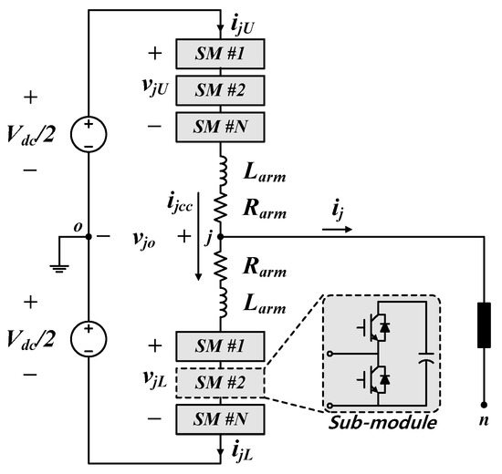
Figure 1.
Single-phase circuit diagram for a modular multilevel converter (MMC).
The structure of SM for MMC could be a half-bridge, full-bridge, clamped double bridge, three-level neutral-point-clamped bridge, five-level cross-connected bridge, etc. [22,23]. The SM with the half-bridge is most commonly used in the commercial HVDC system, although other structures of SM have easy handling capabilities for the DC fault current. So, this paper has only considered the SM with a half-bridge structure.
The upper arm voltage by the switching operation of SMs can be expressed with the product of the turn-on number of SMs and the SM voltage as shown in Equation (1). The lower arm voltage can be expressed with the product of the turn-on number of SMs and the SM voltage as shown in Equation (2).
The currents through the upper- and lower-arms are defined by and , and the line current on each phase can be deduced with Equation (3).
The common circulating current of upper- and lower-arms can be deduced with Equation (4).
The currents on the upper- and lower-arms are respectively expressed with Equations (5) and (6), using the relationship of Equations (3) and (4).
By applying Kirchhoff’s voltage law to the circuit in Figure 1, the terminal voltage can be represented by Equations (7) and (8).
Equation (9) can be induced by relating Equations (3), (7), and (8).
According to Equation (9), the voltage drop is caused by the arm reactor. Its phase angle is equivalent to the lower arm voltage and shifted by 180° from the upper arm voltage .
2.2. Modulation and Harmonic Analysis
MMC normally generates the output voltage with PWM and stepped modulation. In PWM the reference signal is compared with triangular carriers to decide the switching position. In stepped modulation the reference signal is divided into segments with a certain time span and the cross point with the reference signal sets the switching position. Stepped modulation has less switching frequency and the generated output voltage changes less suddenly. Equal area method (EAM), selective harmonic reduction method (SHRM), and NLC are typical stepped modulation schemes. The first two schemes generate relatively low levels of harmonics, but require more computations. So, NLC is most widely used in MMC for high power application [24,25,26].
Figure 2 describes how to generate the output voltage in NLC modulation. NLC applies the rounding-off function to decide the point of level change. NLC generates an output voltage with simple computation close to the sine wave.
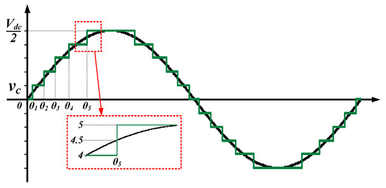
Figure 2.
Operational principle of the nearest level control (NLC) modulation.
When MMC operates in NLC, the operation level can be decided by the magnitude of MI which is determined by the ratio of AC voltage to DC voltage.
The terminal voltage command on the upper- and lower-arms can be defined by the cosine function and MI, thereby being expressed as Equations (11) and (12).
Figure 3 shows a block diagram for the NLC, and the number of SMs is decided by inputting the voltage command of upper- and lower-arm and rounding off. This method does not support equal charging and discharging for each SM during one power cycle. So, the voltage balancing algorithm for the SM capacitors is required [17,18,19,20].
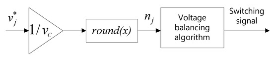
Figure 3.
Block diagram for NLC modulation.
The voltage level is an important factor in NLC because it influences the average switching time and the THD of output voltage.
Fourier series for the waveform shown in Figure 2 can be expressed as the following equation.
Since the harmonic components only include the odd number of order. The root mean square (RMS) values for the fundamental component and the harmonic components can be expressed as the following equations.
THD of the output voltage is defined by the following equation.
Figure 4 shows calculated THDs for the output voltage with respect to the number of voltage levels when the voltage level is located at 9 ≤ N ≤ 200. The THD of the output voltage stays as low as less than 1% if the voltage level is over 40. However, the THD of output voltage is largely changed if the voltage level is lower than 40.
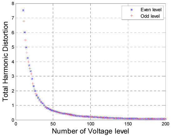
Figure 4.
Total harmonic distortion (THD) according to output voltage level.
Figure 5 shows THD calculation results when the range of MI is set at 0.6 ≤ MI ≤ 1, and in the case that the maximum voltage level is assigned to 10~25, THD can be reduced as the voltage level increases and the MI also increases. However, it decreases nonlinearly in a specific range, which is caused by the voltage level suddenly changing due to the MI. The timing of this change can be expressed by Equation (16) according to the variable range of MI.
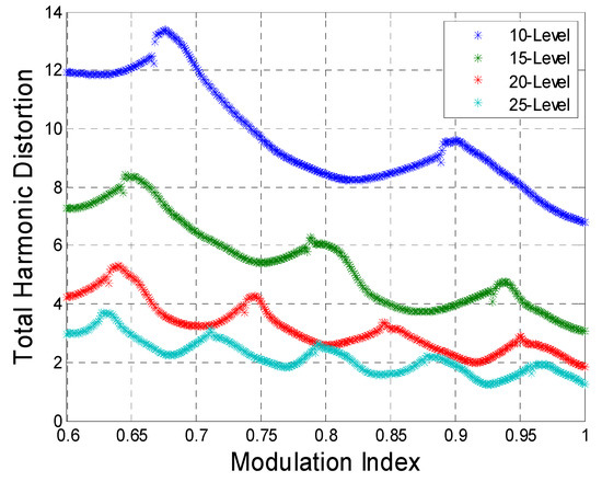
Figure 5.
THD with respect to modulation index (MI) according to number of SMs.
3. Existing Modulation Scheme
Figure 6 shows an equivalent circuit for the MMC operated in NLC. The most traditional scheme is to generate the pole voltage same as the phase voltage command, which is called the sinusoidal modulation. In this case, the maximum phase voltage is limited to the half of the DC voltage. It can be linearly controlled until MI becomes 1, but it shows non-linear output when MI is over 1. The space vector modulation was a typical scheme to improve the sinusoidal modulation with offset voltage control [27,28,29,30].
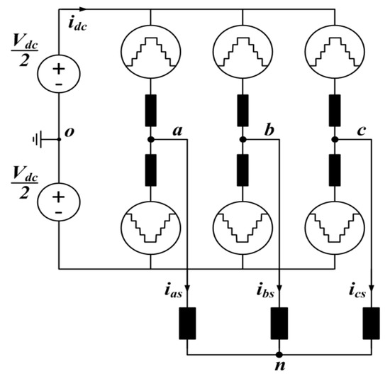
Figure 6.
Equivalent Circuit for MMC operated in NLC.
The pole voltage which is the sum of the phase voltage and the offset voltage can be decided by the switching status of SM on each phase of MMC.
To implement the space vector modulation, the absolute values of maximum and minimum pole voltage should be identically set as Equation (18). In this way, the offset voltage is defined as Equation (19).
In the space vector modulation, the offset voltage is linearly controlled until the MI is equal to . So, the magnitude of output voltage can be enlarged by 15.47% in comparison with the sinusoidal modulation. The reason is that the pole voltage decreases by the offset voltage which is one-sixth of the fundamental component. However, the decrease of MMC output voltage level causes an increase of the average switching frequency, capacitor voltage ripple, and output voltage THD.
4. Proposed Modulation Scheme
This paper proposes a new scheme to compensate the decrease of the output voltage level so as to generate a constant pole voltage irrespective of the magnitude of MI. The proposed method uses a variable offset voltage which is represented by Equation (20).
is a variable to make the pole voltage constant. It can be induced by using the maximum value equation of the pole voltage and can be divided into two regions by the value of MI.
At first, the value of has been analyzed in the region of 1 ≤ MI ≤ , where the pole voltage becomes smaller than the phase voltage due to the offset voltage. Figure 7a shows the pole voltage, phase voltage, and offset voltage in this region.
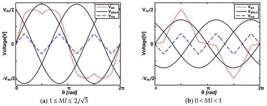
Figure 7.
Pole, Phase, and Offset voltages according to MI.
Equations (21)–(23) express the phase voltage with MI and DC voltage.
The pole voltage has four cases according to its phase angle. Equations (24)–(27) represent the pole voltages at each section.
In order to obtain the maximum value of pole voltage, derivatives for the above equations have to be derived, which are expressed by Equations (28)–(31).
From the above equations, the phase angle of the pole voltage is calculated as Equations (33)–(36).
The maximum value of pole voltage at and can be obtained from Equations (34) and (35). The maximum value of pole voltage at this range is represented by Equation (37), and can be derived by Equation (38).
In the second, the value of has been analyzed in the region of 0 < MI < 1, where the pole voltage becomes larger than the phase voltage because of offset voltage. Figure 7b shows the pole voltage, phase voltage, and offset voltage in this region. The pole voltage always stays at the maximum value in the phase angle of .
In this section, the pole voltage can be defined as Equation (39).
where, is equal to at .
From Equation (32) is derived as the following equation.
So, the maximum value of pole voltage is represented by (41). From this equation the value of can be calculated as shown in Equation (42).
Figure 8 shows a graph that is describing the value of with respect to the range of MI. The graph shows that has negative value when MI is smaller than 1.0, while it has positive value when MI is larger than 1.0.
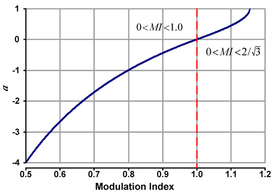
Figure 8.
Variable with respect to MI.
Figure 9 shows the algorithm of the proposed offset voltage control including the NLC modulation. The reference of phase voltage is set through sensing the voltage and current and conducting the current control. is decided according to the value of MI. The references of offset voltage and pole voltage are decided by Equations (20) and (17) respectively. The reference of the pole voltage is passed through the NLC algorithm to obtain the switching pulses. The algorithm of the proposed offset voltage control can be easily implemented on the digital signal processor (DSP) board for real-time operation because it does not require a long running time.
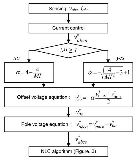
Figure 9.
Flowchart of proposed method.
5. Computer Simulation
In order to verify the proposed scheme, simulation model has been implemented with PSCAD/EMTDC software. The circuit parameters for the simulation model are described in Table 1. The proposed offset voltage control has been implemented using the C-code interface module.

Table 1.
Circuit Parameters for Simulation Model.
Figure 10 shows the simulation results for the sinusoidal modulation. The pole voltage, phase voltage, offset voltage, and line-to-line voltage are shown according to the change of MI. When the MI decreases from to 0.8 with a constant slope, the output voltage level for NLC is decided by Equations (43) and (44). Therefore, the pole voltage decreases to 11-level, where the MI is less than 0.9167 because the MMC is designed to be 13-level.
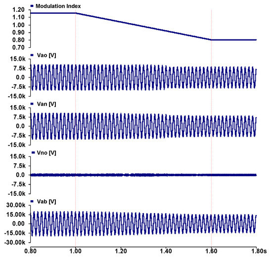
Figure 10.
Simulation waveform with sinusoidal method.
Figure 11 shows simulation results for the space vector modulation. In this modulation, the output voltage level is decided by Equations (45)–(47) according to the range of MI. Therefore, the pole voltage decreases to 11-level, where the MI is less than 1.058. It becomes 9-level, where the MI is less than 0.866.
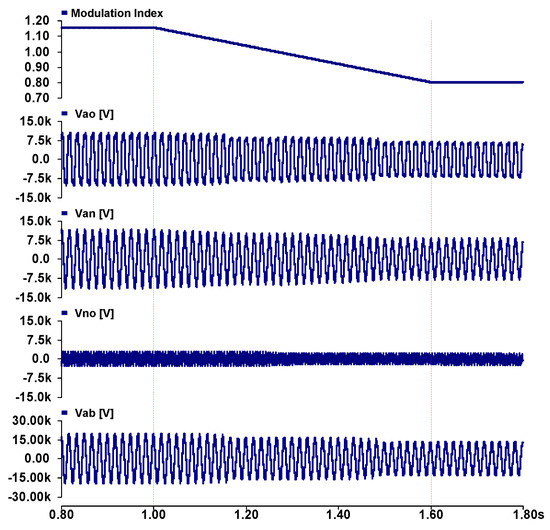
Figure 11.
Simulation waveform with space vector method.
Figure 12 shows the simulation results for the proposed NLC modulation. In this modulation, the output voltage level is maintained at 13-level in all range of MI. The phase voltage becomes the difference between the pole voltage and the offset voltage. The phase voltage and the line-to-line voltage are linearly generated, which is different from the previous two modulations.
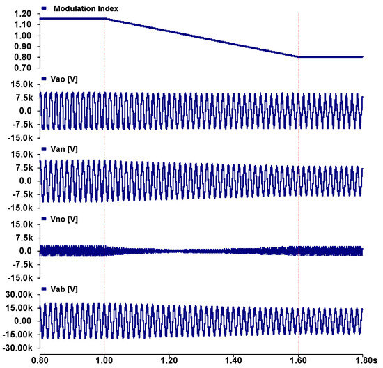
Figure 12.
Simulation waveform with proposed method.
Figure 13 describes the expanded waveform for the pole voltage, phase voltage, and offset voltage for two values of MI. Figure 13a shows that the phase voltage can be linearly generated at the MI > 1 by controlling the offset voltage. Also, Figure 13b shows that the pole voltage is generated at the maximum value that is half of the DC voltage. So, the output voltage is generated with 13-level at the MI = 0.8 by controlling the offset voltage.
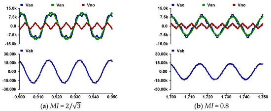
Figure 13.
Expanded waveforms with proposed scheme.
Table 2 shows the comparison results for three modulation schemes. The proposed scheme maintains the pole voltage level constant irrespective of the change of MI. This offers ripple reduction of the SM capacitor voltage and THD reduction of the phase voltage.
Table 2.
Comparison of modulation schemes.
6. Experimental Verification
To verify the proposed scheme though experimental results, a scaled hardware was built in the lab, with circuit parameters that are described in Table 3. In the scaled hardware, each phase has 24 SMs, which is 12 SMs for each upper- and lower-arm. In total 72 SMs are mounted in the rack for implementing 3-phase MMC. The controller consists of one master controller and six arm controllers which were developed by DSP boards based on TMS320F28335. All command signals are delivered down to arm controllers from the master controller.
Table 3.
Circuit Parameters for scaled Hardware.
Figure 14 shows the experimental results for the sinusoidal modulation, which show the pole voltage, phase voltage, and offset voltage according to the change of MI. When the MI decreases from to 0.8 with constant slope, the pole voltage decreases to 11-level where the MI is less than 0.9167.
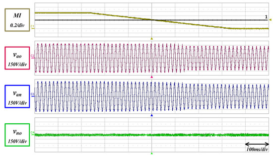
Figure 14.
Hardware waveform with sinusoidal method.
Figure 15 shows the experimental results for the space vector modulation when the MI is changed with same way. The output voltage was checked to become 11-level where the MI is less than 1.058. Also, it was checked to become 9-level where the MI is less than 0.866.
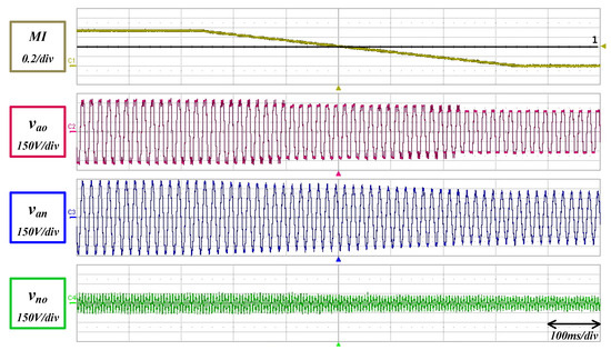
Figure 15.
Hardware waveform with space vector method.
Figure 16 shows the experimental results for the proposed modulation, when the MI is changed in the same way. The pole voltage shows a constant maximum level in all ranges and the phase voltage is generated by the difference between the terminal voltage and the offset voltage. The generated phase voltage is relatively linear in comparison with other two modulations.
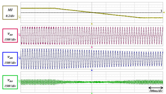
Figure 16.
Hardware waveform with proposed method.
Figure 17a shows expanded waveforms for the pole voltage, phase voltage, line-to-line voltage, and offset voltage when the MMC is operated in 13-level at MI = . The THDs of the pole voltage and the line-to-line voltage are 21.02% and 2.07% respectively. In order to decrease the magnitude of the pole voltage less than the phase voltage, the offset voltage is added. Figure 17b shows the same voltages for when the MMC is operated in 13-level at MI = 0.8. The THDs of the pole voltage and the line-to-line voltage are 22.24% and 2.17% respectively. In order to increase the magnitude of the pole voltage larger than the phase voltage, the offset voltage is added. Both waveforms confirm that the pole has a constant maximum level in all the ranges of MI.
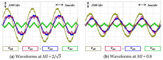
Figure 17.
Expanded waveforms with proposed modulation.
Figure 18 shows the comparison results of THD for three modulation schemes with respect to the MI change. The space vector modulation has the offset voltage that is one-third of fundamental voltage. So, THD of pole voltage has a constant value in the MI range from 0.8 to 1.1547. On the other hand, the THD is changeable in the proposed modulation. The THD of line-to-line voltage shows greater improvement than the other two modulations.
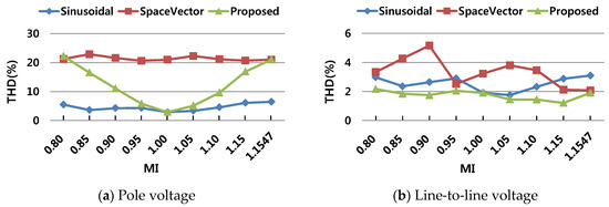
Figure 18.
THD analysis results for three modulation schemes.
Figure 19a shows the active power and reactive power variations with step manner, in which the active power P changes 0, 5, 10, 0 kW and the reactive power changes 0, −10, 0, 10, 0, −10, 0 kVar. The measured active- and reactive-power follow the command values accurately. Figure 19b shows the generated pole voltage which is accurately controlled in magnitude and phase. Figure 19c shows the line current which changes with step manner according to the active- and reactive power change. Figure 19d shows variations of the SM capacitor voltage when the active power is 8 kW and the reactive power −6 kVar. The SM capacitor voltage shows balanced although irregular ripples exist due to the sudden voltage change.
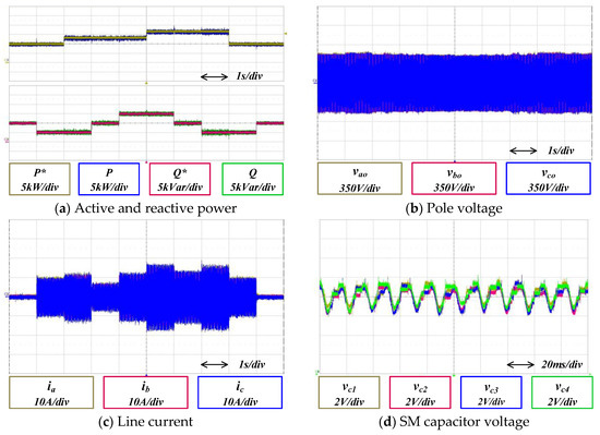
Figure 19.
Major waveforms with proposed method.
7. Conclusions
This paper proposes a new offset voltage control scheme for the MMC operated in NLC to improve the THD of the output voltages and to generate linearly variable phase voltages in the over-modulation region as well as the normal-modulation region.
The feasibility of the proposed scheme was analyzed with computer simulations for the 25 MVA 20 kV MMC with 12 SMs per each arm. Based on the simulation results, a scaled hardware with 10 kVA 1000 V rating was built in the lab and tested to confirm the feasibility of actual implementation. Experimental results also confirm that the proposed offset voltage control is very effective to reduce the THDs of the phase voltage in the whole range of MI. The NLC modulation with proposed offset voltage control is expected to be widely applicable for the MMC of the medium voltage DC system which is composed of relatively smaller numbers of SMs.
Acknowledgments
This work was supported by the National Research Foundation (NRF) grant funded by the Korea Ministry of Science, ICT and Future Planning (NRF-2015R1A2A2A01004102).
Author Contributions
Do-Hyun Kim and Jae-Hyuk Kim proposed the original idea, and carried out computer simulations and experiments. Byung-Moon Han wrote the full manuscript and supervised the simulations and experiments.
Conflicts of Interest
The authors declare no conflict of interest.
Nomenclature
| EAM | Equal area method | Turn-on number of upper arm SMs | |
| HVDC | High voltage direct current | Turn-on number of lower arm SMs | |
| IGBT | Insulated gate bipolar transistor | Output AC voltage | |
| MI | Modulation index | DC link voltage | |
| MVDC | Medium voltage direct current | Pole voltage | |
| N | Number of sub-modules | Phase voltage | |
| NLC | Nearest level control | Pole voltage | |
| PSC | Phase shift carrier | Phase voltage | |
| PWM | Pulse width modulation | Lower arm voltage | |
| SHRM | Selective harmonic reduction method | Upper arm voltage | |
| SM | Sub-module | Maximum value of pole voltage | |
| THD | Total harmonic distortion | Voltage command | |
| Phase current | Upper arm pole voltage reference | ||
| Circulating current | Lower arm pole voltage reference | ||
| Lower arm current | Offset voltage | ||
| Upper arm current | Maximum pole voltage | ||
| a-, b-, c-phase | Minimum pole voltage |
References
- Jacobson, B.; Jiang-Haefner, Y.; Rey, P.; Asplund, G.; Jeroense, M.; Gustatsson, A.; Bergkvist, M. HVDC with Voltage Source Converters and Extrude Cables for Up To +/− 300kV and 1000MW. In Proceedings of the Cigre Meeting 2006, Paris, France, 27 August–1 September 2006. [Google Scholar]
- Dorn, J.; Huang, H.; Tetzmann, D. Novel Voltage-Sourced Converters for HVDC and FACTS Application. In Proceedings of the Cigre Meeting 2007, Paris, France, 25–31 August 2007. [Google Scholar]
- Jacobson, B.; Karlsson, P.; Asplund, G.; Harnefors, L.; Jonsson, T. VSC_HVDC Transmission with cascaded Two-Level Converters. In Proceedings of the Cigre Meeting 2010, Paris, France, 22–27 August 2010. [Google Scholar]
- Nabae, A.; Takahashi, I.; Akagi, H. A New Neutral—Point-Clamped PWM Inverter. IEEE Trans. Ind. Appl. 1981, IA-17, 518–523. [Google Scholar] [CrossRef]
- Railing, B.; Miller, J.; Steckley, P.; Moreau, G.; Bard, P.; Ronstroem, L.; Lindberg, J. Cross Sound Cable Project Second Generation VSC Technology for HVDC. In Proceedings of the Cigre Meeting 2004, Paris, France, 29 August–3 September August 2004. [Google Scholar]
- Peng, F.Z.; Lai, J.S. Dynamic performance and control of a static VAr generator using cascade multilevel inverters. IEEE Trans. Ind. Appl. 1997, 33, 748–755. [Google Scholar] [CrossRef]
- Lesnicar, A.; Marquardt, R. An innovative modular multilevel converter topology suitable for a wide power range. In Proceedings of the 2003 IEEE Power Tech Conference Proceedings, Bologna, Italy, 23–26 June 2003; Volume 3. [Google Scholar]
- Lesnicar, A.; Marquardt, R. A new modular voltage source inverter topology. In Proceedings of the European Power Electronics Conference (EPE), Toulouse, France, 2–4 September 2003. [Google Scholar]
- Franquelo, L.G.; Rodriguez, J.; Leon, J.I.; Kouro, S.; Portillo, R.; Prats, M.A.M. The age of multilevel converters arrives. IEEE Ind. Electron. Mag. 2008, 2, 28–39. [Google Scholar] [CrossRef]
- Marquardt, R. Modular Multilevel Converter: An universal concept for HVDC-Networks and extended DC-Bus Applications. In Proceedings of the IEEE ECCE-Asia IPEC 2010, Sapporo, Japan, 21–24 June 2010. [Google Scholar]
- Gnanarathna, U.; Gole, A.; Jayasinghe, R. Efficient Modeling of Modular Multilevel HVDC Converters on Electromagnetic Transient Simulation Programs. IEEE Trans. Power Deliv. 2011, 26, 316–324. [Google Scholar] [CrossRef]
- Friedrich, K. Modern HVDC PLUS application of VSC in Modular Multilevel Converter Topology. In Proceedings of the IEEE ISIE 2010 International Symposium on Industrial Electronics, Bari, Italy, 4–7 July 2010. [Google Scholar]
- Bergna, G.; Berne, E.; Egrot, P.; Lefranc, P.; Arzande, A.; Vannier, J.; Molinas, M. An Energy-based Controller for HVDC Modular Multilevel Converter in Decoupled Double Synchronous Reference Frame for Voltage Ocillation. IEEE Trans. Ind. Electron. 2013, 60, 2360–2371. [Google Scholar] [CrossRef]
- Mura, F.; de Doncker, W. Design Aspects of a Medium-Voltage Direct Current (MVDC) Grid for a University Campus. In Proceedings of the IEEE ECCE-Asia 2011 8th International Conference on Power Electronics, Jeju, Korea, 30 May–3 June 2011. [Google Scholar]
- Hu, P.; Jiang, D. A Level-Increased Nearest Level Modulation Method for Modular Multilevel Converters. IEEE Trans. Ind. Electron. 2015, 30, 1836–1842. [Google Scholar] [CrossRef]
- Lin, L.; Lin, Y.; He, Z.; Chen, Y.; Hu, J.; Li, W. Improved Nearest-Level Modulation for a Modular Multilevel Converter with a Lower Submodule Number. IEEE Trans. Power Electron. 2016, 31, 5369–5377. [Google Scholar] [CrossRef]
- Tu, Q.; Xu, Z. Impact of Sampling Frequency on Harmonic Distortion for Modular Multilevel Converter. IEEE Trans. Power Electron. 2011, 26, 298–306. [Google Scholar] [CrossRef]
- Park, Y.H.; Kim, D.H.; Kim, J.H.; Han, B.M. A New Scheme for Nearest Level Control with Average Switching Frequency Reduction for Modular Multilevel Converters. J. Power Electron. 2016, 16, 522–531. [Google Scholar] [CrossRef]
- Choi, J.Y.; Han, B.M. New Scheme of Phase-Shifted Carrier PWM for Modular Multilevel Converter with Redundancy Submodules. IEEE Trans. Power Electron. 2016, 31, 407–409. [Google Scholar] [CrossRef]
- Tu, Q.; Xu, Z.; Chang, Y.; Guan, L. Suppressing DC Voltage Ripples of MMC-HVDC under Unbalanced Grid Conditions. IEEE Trans. Power Deliv. 2012, 27, 1332–1338. [Google Scholar] [CrossRef]
- Hanefors, L.; Antonopoulos, A.; Norrga, S.; Aengquist, L.; Nee, H. Dynamic Analysis of Modular Multilevel Converters. IEEE Trans. Ind. Electron. 2013, 60, 2526–2537. [Google Scholar] [CrossRef]
- Nami, A.; Liang, J.; Dijkhuizen, F.; Demetriades, G. Modular Multilevel Converters for HVDC Applications: Review on Converter Cells and Functionalities. IEEE Trans. Power Electron. 2015, 30, 18–36. [Google Scholar] [CrossRef]
- Debnath, S.; Qin, J.; Bahrani, B.; Saeedifard, M.; Barbosa, P. Operation, Control, and Applications of the Modular Multilevel Converter: A Review. IEEE Trans. Power Electron. 2015, 30, 37–53. [Google Scholar] [CrossRef]
- Zhang, Y.; Adam, G.; Lin, T.; Finney, S.; Williams, B. Analysis of modular multilevel converter capacitor voltage balancing based on phase voltage redundant states. IET Power Electron. 2010, 5, 726–738. [Google Scholar] [CrossRef]
- Song, Q.; Liu, W.; Li, X.; Rao, H.; Xu, S.; Li, L. A Steady-State Analysis Method for a Modular Multilevel Converter. IEEE Trans. Power Electron. 2013, 28, 3702–3713. [Google Scholar] [CrossRef]
- Ilves, K.; Antonopoulos, A.; Norrga, S.; Nee, H. A New Modulation Method for the Modular Multilevel Converter Allowing Fundamental Switching Frequency. IEEE Trans. Power Electron. 2012, 27, 3482–3494. [Google Scholar] [CrossRef]
- Seo, J.H.; Choi, C.H.; Hyun, D.S. A new simplified space-vector PWM method for three-level inverters. IEEE Trans. Power Electron. 2001, 16, 545–550. [Google Scholar]
- Blasko, V. A hybrid PWM strategy combining modified space vector and triangle comparison methods. In Proceedings of the PESC Record 27th Annual IEEE Power Electronics Specialists Conference, Baveno, Italy, 23–26 June 1996; Volume 2, pp. 1872–1878. [Google Scholar]
- Chung, D.W.; Kim, J.S.; Sul, S.K. Unified voltage modulation technique for real-time three-phase power conversion. IEEE Trans. Ind. Appl. 1998, 34, 374–380. [Google Scholar] [CrossRef]
- Kim, J.H.; Sul, S.K. A carrier-based PWM method for three-phase four-leg voltage source converters. IEEE Trans. Power Electron. 2004, 19, 66–75. [Google Scholar] [CrossRef]
© 2017 by the authors. Licensee MDPI, Basel, Switzerland. This article is an open access article distributed under the terms and conditions of the Creative Commons Attribution (CC BY) license (http://creativecommons.org/licenses/by/4.0/).