
Influence of Gas Annealing on Sensitivity of AlN/4H-SiC-Based Temperature Sensors

 , and
, and 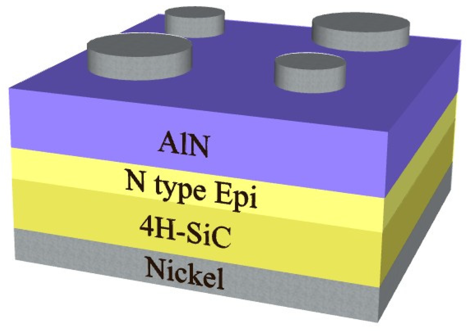
Abstract
1. Introduction
2. Materials and Methods
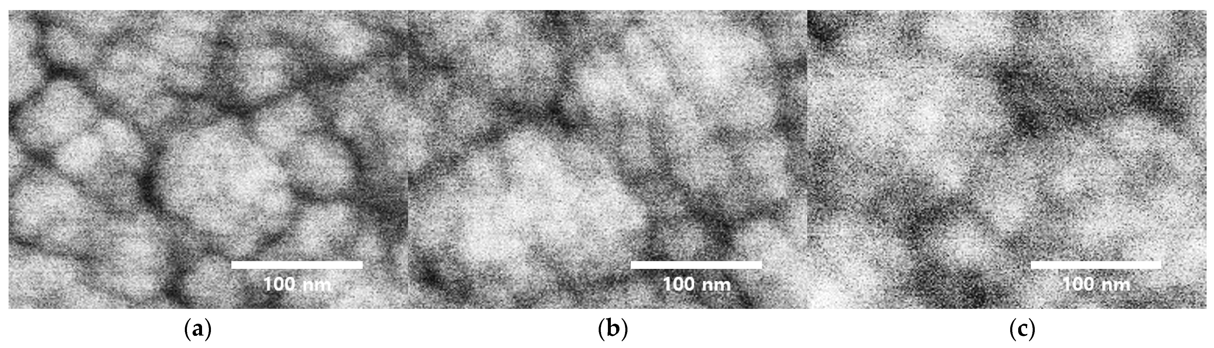
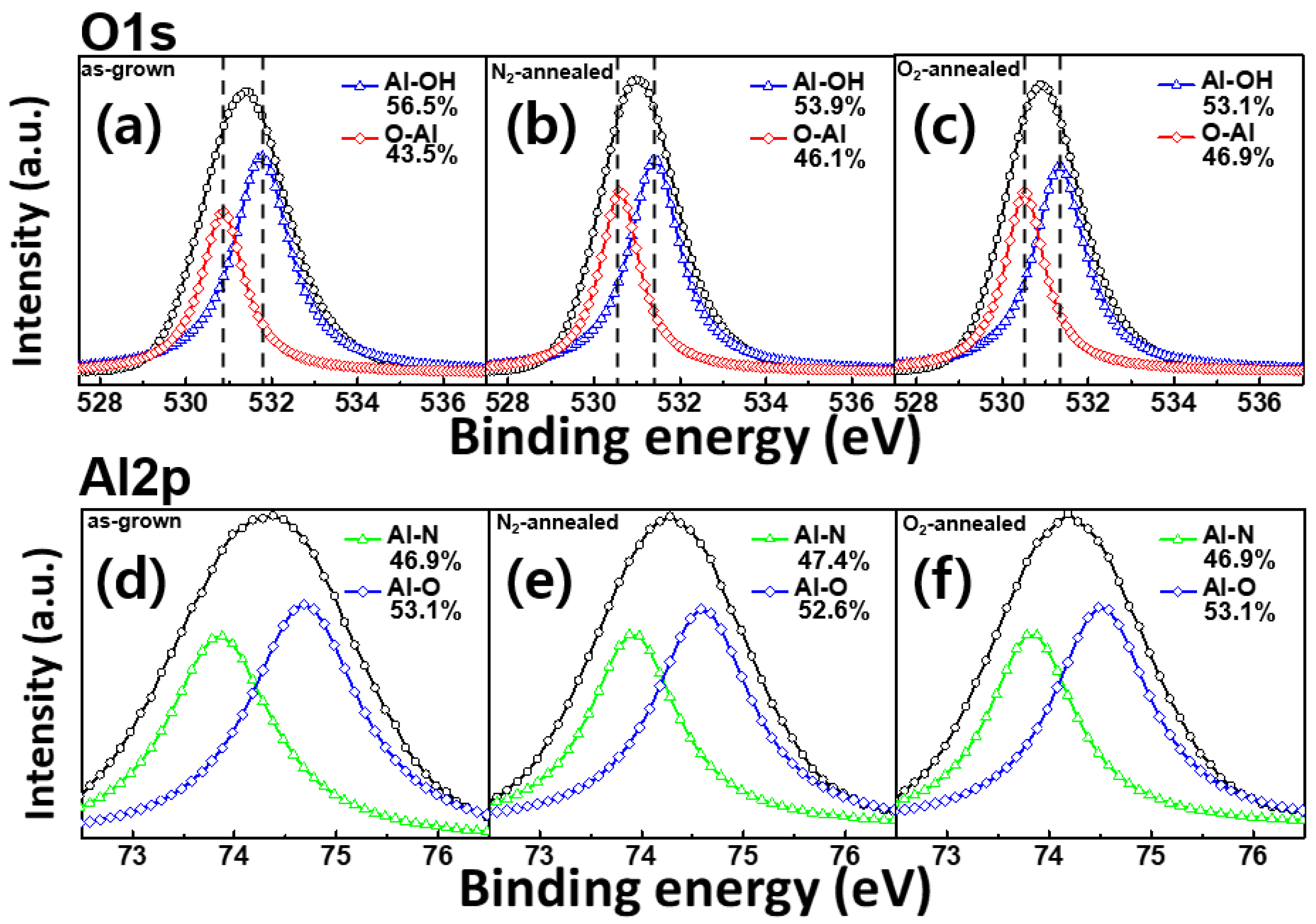
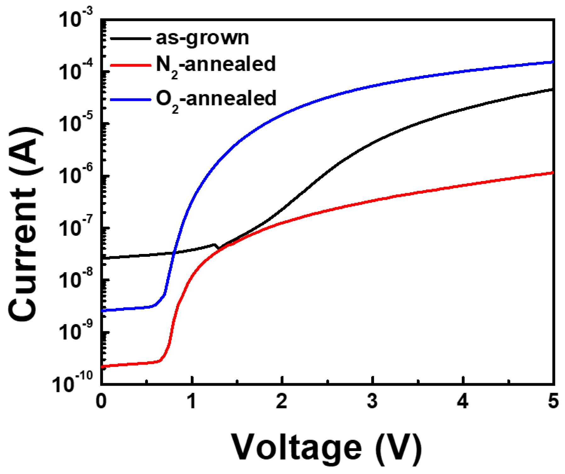
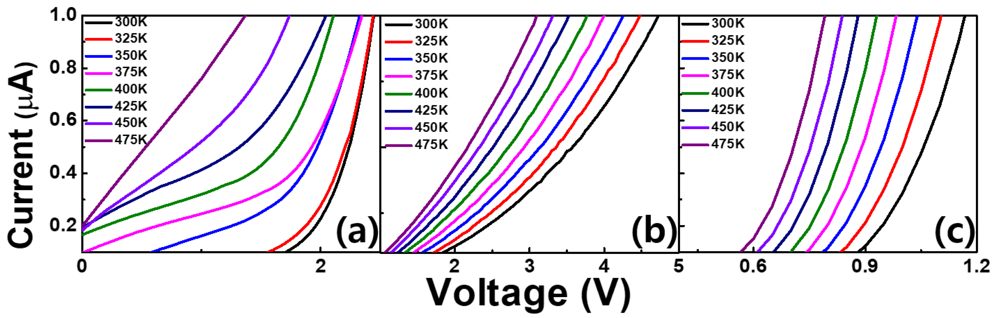
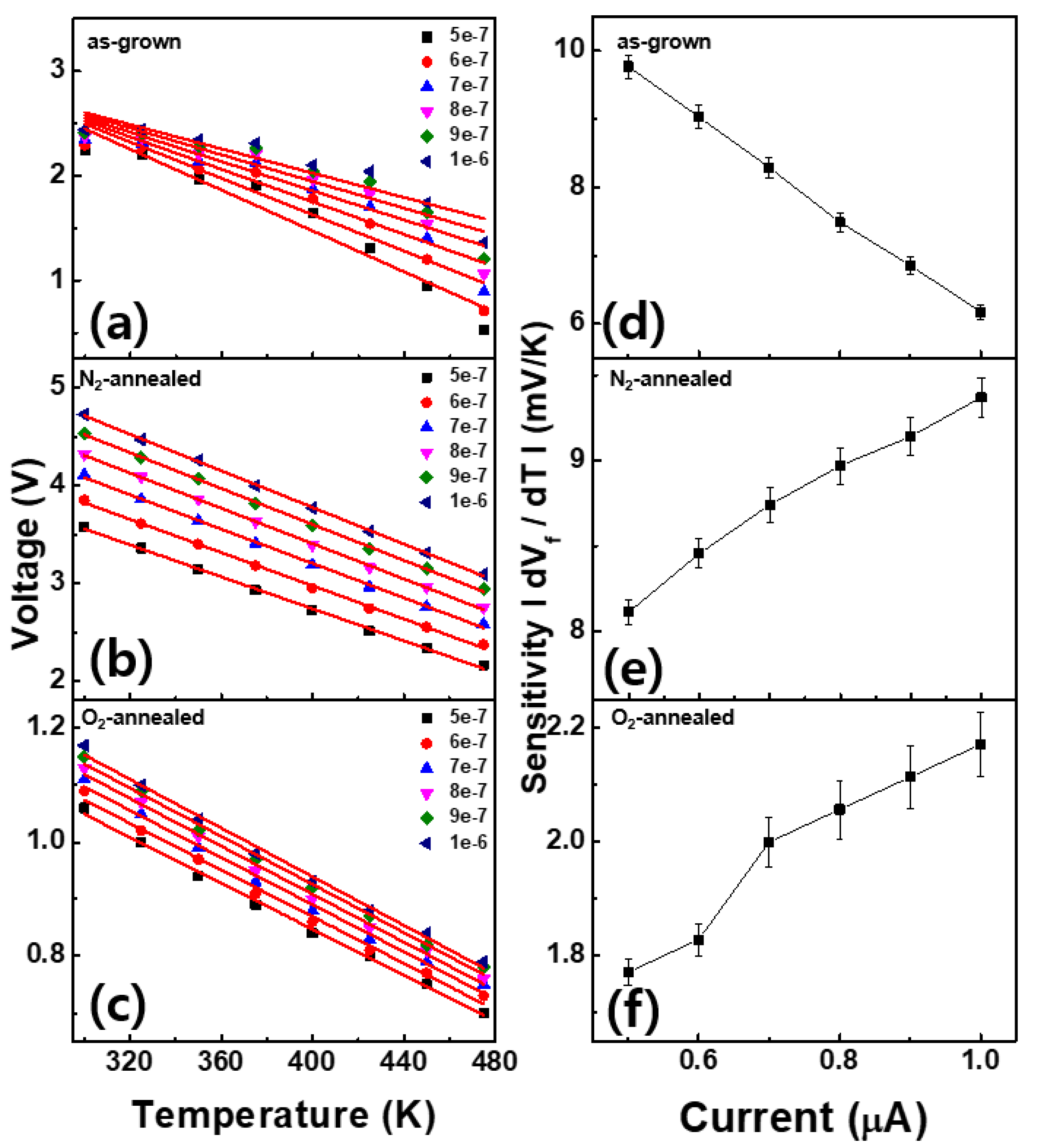
3. Results and Discussion
4. Conclusions
Author Contributions
Funding
Institutional Review Board Statement
Informed Consent Statement
Data Availability Statement
Acknowledgments
Conflicts of Interest
References
- Liang, J.; Nishida, S.; Hayashi, T.; Arai, M.; Shigekawa, N. Effects of interface state charges on the electrical properties of Si/SiC heterojunctions. Appl. Phys. Lett. 2014, 105, 151607. [Google Scholar] [CrossRef]
- Cheng, H.; Sun, Y.; Zhang, J.X.; Zhang, Y.B.; Yuan, S.; Hing, P. AlN films deposited under various nitro-gen concentrations by RF reactive sputtering. J. Cryst. Growth 2003, 254, 46–54. [Google Scholar] [CrossRef]
- Behera, L.; Pandey, N.; Gupta, M. Synthesis and characterization of AlN thin films deposited using DC and RF magnetron sputtering. In DAE Solid State Physics Symposium 2019, AIP Conference Proceedings; AIP Publishing LLC.: Melville, NY, USA, 2020; Volume 2265, p. 030310. [Google Scholar] [CrossRef]
- Kim, D.H.; Min, S.J.; Oh, J.M.; Koo, S.M. Fabrication and Characterization of Oxygenated AlN/4H-SiC Heterojunction Diodes. Materials 2020, 13, 4335. [Google Scholar] [CrossRef] [PubMed]
- Tanaka, S.; Shojiki, K.; Uesugi, K.; Hayashi, Y.; Miyake, H. Quantitative evaluation of strain relaxation in annealed sputter-deposited AlN film. J. Cryst. Growth 2019, 512, 16–19. [Google Scholar] [CrossRef]
- Miyake, H.; Lin, C.-H.; Tokoro, K.; Hiramatsu, K. Preparation of high-quality AlN on sapphire by high-temperature face-to-face annealing. J. Cryst. Growth 2016, 456, 155–159. [Google Scholar] [CrossRef]
- Benmoussa, A.; Soltani, A.; Schuhle, U.; Haenen, K.; Chong, Y.; Zhang, Y.-L.; Dahal, R.; Lin, J.Y.; Jiang, H.; Barkad, H.; et al. Recent developments of wide-bandgap semiconductor based UV sensors. Diam. Relat. Mater. 2009, 18, 860–864. [Google Scholar] [CrossRef]
- Liu, G.; Yan, C.; Zhou, G.; Qin, Z.; Zhou, Q.; Zheng, R.; Sun, Z. Defects induced broad spectral photore-sponse of PVT-grown bulk AlN crystals. Scr. Mater. 2018, 154, 45–48. [Google Scholar] [CrossRef]
- Rahman, H.; Thakur, J.S.; Rimai, L.; Perooly, S.; Naik, R.R.; Zhang, L.; Auner, G.W.; Newaz, G. Dual-mode operation of a Pd/AlN/SiC device for hydrogen sensing. Sensor. Actuator. B Chem. 2008, 129, 35–39. [Google Scholar] [CrossRef]
- Min, S.J.; Shin, M.C.; Thi Nguyen, N.; Oh, J.M.; Koo, S.M. High-performance temperature sensors based on dual 4H-SiC JBS and SBD devices. Materials 2020, 13, 445. [Google Scholar] [CrossRef]
- Le, X.; Wang, X.; Pang, J.; Liu, Y.; Fang, B.; Xu, Z.; Gao, C.; Xu, Y.; Xie, J. A high performance humidity sensor based on surface acoustic wave and graphene oxide on AlN/Si layered structure. Sensor. Actuator. B Chem. 2018, 255, 2454–2461. [Google Scholar] [CrossRef]
- Jung, J.C.; Koo, S.M. The Effect of Catalytic Metal Work Functions and Interface States on the High Tem-Perature SiC-Based Gas Sensors. J. Korean Inst. Electr. Electron. Mater. Eng. 2011, 24, 280–284. [Google Scholar]
- Li, D.; Song, X.; Xu, J.; Wang, Z.; Zhang, R.; Zhou, P.; Zhang, H.; Huang, R.; Wang, S.; Zheng, Y.; et al. Optical properties of thickness-controlled MoS2 thin films studied by spectroscopic ellipsometry. Appl. Surf. Sci. 2017, 421, 884–890. [Google Scholar] [CrossRef]
- Rao, T.P.; Kumar, M.S. Resistivity Stability of Ga Doped ZnO Thin Films with Heat Treatment in Air and Oxygen Atmospheres. J. Cryst. Process. Technol. 2012, 2, 72–79. [Google Scholar] [CrossRef]
- Xiang, Y.; Zhou, C.; Jia, E.; Wang, W. Oxidation precursor dependence of atomic layer deposited Al2O3 films in a-Si:H(i)/Al2O3 surface passivation stacks. Nano. Res. Letter. 2015, 10, 1–8. [Google Scholar] [CrossRef] [PubMed]
- Cao, D.; Cheng, X.; Xie, Y.-H.; Zheng, L.; Wang, Z.; Yu, X.; Wang, J.; Shen, D.; Yu, Y. Effects of rapid thermal annealing on the properties of AlN films deposited by PEALD on AlGaN/GaN heterostructures. RSC Adv. 2015, 5, 37881–37886. [Google Scholar] [CrossRef]
- Kale, A.; Brusa, R.; Miotello, A. Structural and electrical properties of AlN films deposited using reactive RF magnetron sputtering for solar concentrator application. Appl. Surf. Sci. 2012, 258, 3450–3454. [Google Scholar] [CrossRef]
- Kumar, V.; Maan, A.S.; Akhtar, J. Barrier height inhomogeneities induced anomaly in thermal sensitivity of Ni/4H-SiC Schottky diode temperature sensor. J. Vac. Sci. Technol. B 2014, 32, 041203. [Google Scholar] [CrossRef]
- Bakker, A.; Huijsing, J. Micropower CMOS temperature sensor with digital output. IEEE J. Solid State Circuits 1996, 31, 933–937. [Google Scholar] [CrossRef]
- Li, L.; Li, X.; Pu, T.; Cheng, S.; Li, H.; Ao, J.P. Vertical Gan-based Temperature Sensor by Using TiN Anode Schottky Barrier Diode. IEEE Sensor. J. 2020, 21, 1273–1278. [Google Scholar] [CrossRef]
- Guo, Q.; Lu, F.; Tan, Q.; Zhou, T.; Xiong, J.; Zhang, W. Al2O3-Based a-IGZO Schottky Diodes for Tempera-ture Sensing. Sensors 2019, 19, 224. [Google Scholar] [CrossRef] [PubMed]


Publisher’s Note: MDPI stays neutral with regard to jurisdictional claims in published maps and institutional affiliations. |
© 2021 by the authors. Licensee MDPI, Basel, Switzerland. This article is an open access article distributed under the terms and conditions of the Creative Commons Attribution (CC BY) license (http://creativecommons.org/licenses/by/4.0/).
Share and Cite
Jung, S.-W.; Shin, M.-C.; Schweitz, M.A.; Oh, J.-M.; Koo, S.-M. Influence of Gas Annealing on Sensitivity of AlN/4H-SiC-Based Temperature Sensors. Materials 2021, 14, 683. https://doi.org/10.3390/ma14030683
Jung S-W, Shin M-C, Schweitz MA, Oh J-M, Koo S-M. Influence of Gas Annealing on Sensitivity of AlN/4H-SiC-Based Temperature Sensors. Materials. 2021; 14(3):683. https://doi.org/10.3390/ma14030683
Chicago/Turabian StyleJung, Seung-Woo, Myeong-Cheol Shin, Michael A. Schweitz, Jong-Min Oh, and Sang-Mo Koo. 2021. "Influence of Gas Annealing on Sensitivity of AlN/4H-SiC-Based Temperature Sensors" Materials 14, no. 3: 683. https://doi.org/10.3390/ma14030683
APA StyleJung, S.-W., Shin, M.-C., Schweitz, M. A., Oh, J.-M., & Koo, S.-M. (2021). Influence of Gas Annealing on Sensitivity of AlN/4H-SiC-Based Temperature Sensors. Materials, 14(3), 683. https://doi.org/10.3390/ma14030683