Abstract
This work presents a systematic design flow for the fundamental building blocks (namely, the low-noise amplifier and the down-conversion mixer) of an analog receiver for 5G backhauling systems implemented in SiGe BiCMOS technology. The proposed methodology enables the sizing and optimization of receiver blocks up to post-layout simulations, starting from the specified performance requirements. It accounts for both the parasitic effects of active devices and the distributed effects of interconnects. The design flow was applied using STMicroelectronics BiCMOS55X technology to develop low-noise amplifiers and D-band to E-band downconverters capable of covering the 130–150 GHz and 150–165 GHz sub-bands. Preliminary measurement results obtained from both the standalone LNA blocks and the complete receivers are presented and discussed.
1. Introduction
The increasing demand for capacity in mobile networks, together with the development of high-resolution radar sensors, can be addressed by expanding the available bandwidth, thereby driving the design of systems operating in the E-band and D-band. In particular, for the backhauling section of point-to-point millimeter-wave radio links [1], channel bandwidths of up to 2 GHz can be achieved in the E-band. For cases in which even wider bandwidths are required and/or multiple non-overlapping channels are needed to support data rates approaching 100 Gb/s [2], the four non-contiguous frequency bands allocated in the D-band for wireless services are being investigated as a promising solution [2,3,4], owing to their relatively low atmospheric absorption (<2 dB/km). However, while increasing the carrier frequency enhances communication capacity, it also makes transceiver circuit design significantly more challenging. As the carrier frequency approaches the technology transition frequency fT, achieving the required performance in terms of noise, gain, linearity, and output power becomes more difficult—especially over wide bandwidths. In this context, BiCMOS technologies based on heterojunction bipolar transistors (HBTs) have attracted growing interest for millimeter-wave circuit design, leveraging fT and fMAX values exceeding 200 GHz. These processes [5,6,7] combine the high-frequency performance of bipolar transistors—essential for front-end analog circuits—with millimeter-wave low-loss passive components (inductors, capacitors, and transmission lines), as well as CMOS technology, enabling the integration of analog-to-digital and digital-to-analog converters and low-power digital logic.
The main building blocks of D-band receivers—namely the LNA [8,9,10,11,12,13,14,15,16,17,18], the variable gain amplifier (VGA) [19,20], and the mixer [21,22,23,24,25,26]—have been successfully demonstrated in recent years using SiGe BiCMOS technologies. It is worth noting that the VGA plays a key role in the receiver chain, as it enables compliance with system dynamic range requirements without operating near compression, thereby preventing BER degradation due to intermodulation distortion [3]. Furthermore, a four-channel receiver and a four-channel transmitter for phased-array transceivers were prototyped on a single BiCMOS chip [4]. Link budget analysis and block-level performance requirements—expressed in terms of BER, EVM, and intermodulation distortion for high-order modulation schemes (up to 256-QAM) [3]—highlight the importance of topology selection and the associated design challenges. Several contributions have focused on design methodologies and topology comparisons. For example, references [11,14] compare common-emitter and cascode stages for D-band amplifier design in BiCMOS technology, evaluating achievable gain–bandwidth product and output matching design complexity. Although the cascode topology provides significantly higher gain, its higher output resistance complicates broadband matching to 50 Ω; therefore, dedicated output matching solutions were proposed. For cascode stages, particular attention has been given to the RF termination of the common-base device. While a shunt capacitance ensures AC grounding, additional techniques—such as series transmission lines acting as inductors [10] or zero-ohm lines [16]—have been introduced to improve LNA performance. A comparison between common-emitter and common-base stages in terms of linearity was presented in [27], targeting D-band power amplifier applications. Moreover, a stacked common-base topology was proposed in [18] as an alternative to differential architectures for the first receiver stage, enabling broadband input matching without area-consuming Marchand baluns. Guidelines for transistor sizing and current density selection were also provided to balance input matching, gain, and Noise Figure (NF). Other previously cited works have similarly proposed both topological solutions—such as inductive emitter degeneration or inductive interstage matching in cascode configurations—and practical design guidelines to enhance overall performance.
In this paper, a comprehensive design flow for D-band receiver building blocks in BiCMOS technology is proposed and experimentally validated through the design and characterization of a D-band LNA and a D-band-to-E-band downconverter incorporating the LNA. The proposed methodology covers all major stages of receiver block development, including device sizing and bias optimization, core circuit synthesis, layout-aware design, electromagnetic (EM) parasitic extraction, matching network implementation, and post-layout verification with process–voltage–temperature (PVT) and Monte Carlo analyses. The remainder of the paper is organized as follows: Section 2 introduces the proposed design flow and describes its individual steps. Section 3 presents the design of a two-stage D-band LNA and D-band down-converting mixers in BiCMOS technology, developed using the proposed methodology. Section 4 reports the experimental characterization of the fabricated blocks, comparing measurement results with simulations. Finally, Section 5 concludes the paper and outlines directions for future research.
2. A Comprehensive Design Flow for D-Band BiCMOS Receiver Blocks
A comprehensive design flow (see Figure 1) is proposed for the development of active receiver building blocks—such as LNA, VGA, or mixer—based on a selected topology and specified performance requirements, including transducer gain GT, NF, third-order intercept point (IP3), return loss, etc. In this section, the design flow is described with reference to the Cadence Virtuoso environment; however, the methodology is general and can be implemented in other design platforms as well.
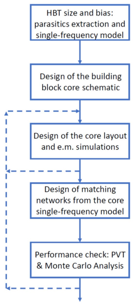
Figure 1.
The proposed flow diagram for the design of D-band receiver building blocks.
The first step consists of selecting the optimal device sizing and current density to achieve the best trade-off among transition frequency fT, minimum Noise Figure NFmin, and linearity metrics, such as the 1 dB compression point and—most importantly—the level of third-order intermodulation distortion. The performance of the LNA, in terms of transducer gain, Noise Figure, and IP3, strongly influences overall system metrics such as BER and EVM, which are defined according to the selected modulation scheme [3]. At this preliminary stage, a dedicated layout of the device under test must be implemented, followed by parasitic extraction. This step is essential to ensure that the design is based on a realistic device model that includes layout-induced parasitic effects. It should be emphasized that the active device under test is often not a single HBT, but rather a composite structure consisting of multiple transistors—for example, a cascode stage or a stacked common-base configuration. For a given device (or composite structure), an approximate evaluation of the transition frequency fT can be obtained from the short-circuit current gain AI. Specifically, for a selected bias current, fT corresponds to the frequency at which the magnitude of AI becomes equal to unity (0 dB). Subsequently, a parametric analysis versus bias current must be performed to determine the operating point that maximizes fT.
The second step of the design flow involves the design of the block core, i.e., the (composite) device together with its output load, excluding the matching networks. For example, this core block may consist of a cascode device with a tuned load for a D-band amplifier, a Gilbert-cell mixer with a resistive (or inductive) load for D-band down-conversion to baseband (or to an intermediate frequency), or a cascode differential pair with a tuned load. Passive components—such as inductors or zero-ohm transmission lines at the base of the common-base device in a cascode topology, or inductive/resistive degeneration at the emitter—can be incorporated into the composite device under test, following the techniques described in Section 1 or newly proposed approaches. At this stage, the output load and any additional passive components are selected to achieve the best trade-off among fT, NFmin, and IP3 in accordance with the system requirements.
First, a single-frequency model is derived for the selected three-terminal composite device, following the scheme shown in Figure 2. The model includes the transconductance (gm), the input resistance (Rin) and capacitance (Cin) modeled in parallel, and similarly, the output resistance (Rout) and capacitance (Cout). These parameters are extracted by biasing the devices at the chosen operating current density and performing S-parameter simulations. The values of gm, Rin and Cin, and Rout and Cout are then derived from the simulated Y-parameters at the design frequency. Although broadband effects, such as feedthrough capacitances, are not fully captured, the model provides sufficient accuracy for narrowband D-band circuit design while significantly simplifying the preliminary design phase. Using this model, the designer can proceed with an analytical (pencil-and-paper) evaluation of the output load components. In particular, the device transconductance gain (gm) and the output impedance Rout//Cout are used to determine the gain, the −3 dB bandwidth, and the center frequency of the core stage. In the case of a tuned load, it consists of a parallel combination of a resistor RC, a capacitor CC, and an inductor LC. The unloaded quality factor QUN can be expressed in terms of the capacitor CC and the resistor RC of the tuned load as follows:
where ω0 is the desired angular resonant frequency. The external capacitor CC is introduced to ensure that the resonance frequency is not determined solely by the parasitic capacitance Cout.
QUN = ω0 × (Cout + CC) × (RCmax//Rout),
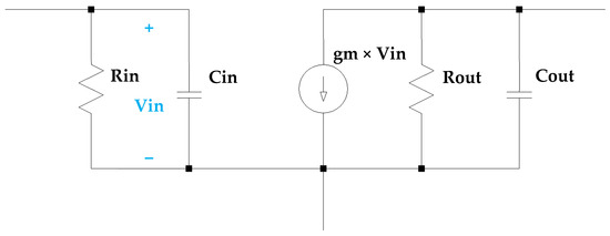
Figure 2.
Single frequency equivalent model of a 3-terminal composite active device.
The loaded quality factor QL is determined by the specified bandwidth:
QL = f0/BW
The loaded quality factor QL can be directly related to the unloaded quality factor QUN, thus enabling the determination of the maximum allowable value of RC (denoted as RCmax) that ensures a bandwidth greater than or equal to the specified BW. In particular, under the assumption of conjugate matching to the external load Rload (i.e., Rload = Rout//RC), the relationship QL = QUN/2 holds. The resistor RC is therefore selected close to RCmax, typically slightly lower, in order to provide a design margin with respect to the specified bandwidth. The value of the tuning inductance LC is determined so as to achieve resonance at the specified angular frequency ω0:
ω02 = 1/[LC × (CC + Cout)],
Finally, small-signal, noise, and harmonic balance simulations of the designed core are performed using the transistor models provided by the foundry in order to verify the performance in terms of maximum available gain (MAG), NFmin and IP3. If the required specifications are not met, the procedure is iterated by modifying the passive components of the composite device, re-extracting the single-frequency model, re-evaluating the output load, and reassessing the core performance in terms of MAG, NFmin and IP3. At the conclusion of this phase, the core block is fully designed. Its robustness is then evaluated by means of PVT and Monte Carlo analyses.
The third step concerns the layout design of the core block. The core is defined as the active device(s) together with the actual biasing network(s), and it also includes the tuned load, degeneration elements, and compensation network, if present. Matching networks are not considered at this stage. The layout is designed after replacing the ideal passive components with the corresponding components from the design kit. Their interconnections are then implemented using the available metal layers. These interconnections must be designed to minimize their length and, consequently, their parasitic effects, thereby avoiding excessive performance degradation with respect to the previously designed lumped-element circuit. Compliance with the foundry design rules is first verified through an automatic Design Rule Check (DRC). Subsequently, consistency between the layout netlist and the original schematic netlist is verified by means of an automatic Layout Versus Schematic (LVS) analysis. Performance verification is then carried out using EM simulations of the interconnections. To this end, a dedicated layout is prepared in which all lumped active and passive components (transistors, resistors, inductors, and capacitors) are removed and replaced with 50 Ω ports. Additional ports are inserted at the input and output of the core. Each of these ports consists of two terminals: a signal pin on an upper metal layer and a ground pin on a lower metal layer. The ground pin is made significantly wider than the signal pin so that the overall structure emulates the behavior of a microstrip line. In the Cadence environment, each terminal of the input and output ports is implemented as a separate 50 Ω port. The result of the EM simulation is an N-port scattering matrix. A new circuit is then assembled, including the extracted N-port matrix together with the lumped active and passive components properly connected. This circuit is simulated to evaluate the core performance, now accounting for the parasitic effects of the interconnections. At this stage, minor adjustments to the tuned load values may be required to ensure that the condition expressed in Equation (3) is satisfied at the specified angular frequency ω0.
The subsequent step involves the design of the matching networks; there may be two or three networks depending on the block functionality (e.g., LNA or mixer). Possible topologies include single-stub networks, three-element lumped networks (π or T configurations), and coupled-line transformers, selected according to the required fractional bandwidth and impedance transformation ratio. The design procedure follows an approach similar to that adopted for the core and makes use of selected parameters (Rin, Cin, Rout, and Cout) extracted from the single-frequency model of the previously designed core. First, an ideal output matching network is synthesized based on Rout and Cout, assuming a 50 Ω termination at its input. Subsequently, an ideal input matching network is designed using Rin and Cin, evaluated for the core terminated with the previously designed output matching network. If necessary, the procedure may be iterated to improve the performance in terms of matching. The layout of the matching networks is then developed and optimized through EM simulations, following a procedure analogous to that described for the core layout, with iterative refinement if required.
The final step consists of assessing the overall circuit performance. This is accomplished by simulating a complete circuit comprising the EM-extracted S-parameter matrices of both the core and the matching networks, together with all lumped components. At this stage, PVT and Monte Carlo analyses are again performed to verify the robustness of the final design and to ensure an acceptable production yield.
3. Design of D-Band LNAs and of D-Band-to-E-Band Downconverters
A D-band LNA and a down-conversion mixer from the D-band to the E-band were designed in SiGe BiCMOS technology following the design flow described in Section 2, with the objective of covering an input bandwidth ranging from 130 GHz to 165 GHz. The design was carried out in the Cadence Virtuoso environment, using the Spectre simulator for linear and harmonic balance analyses and the EMX tool for EM simulations. The simulation models and layout views of both active and passive devices were provided by the foundry as part of the process design kit (PDK). After a preliminary analysis of the system requirements and candidate topologies, the overall frequency range was divided into two sub-bands: a low band (130–150 GHz) and a high band (150–165 GHz). Consequently, one LNA and one down-conversion mixer were designed for each of the two sub-bands.
3.1. D-Band LNA Design
For each of the two sub-bands, a two-stage LNA was designed using a single-stage core based on a cascode topology with a tuned load, as shown in Figure 3. Both stages were matched to 50 Ω to ensure straightforward cascadability. Following a comparison among different emitter areas and device configurations, a cascode composite device employing 4 μm, two-finger transistors was selected in order to meet the specified output 1 dB compression point. As commonly observed, a trade-off exists between Nfmin and gain, which is closely related to the selected current density. In practice, it is advantageous to bias the device at a current density lower than that corresponding to the maximum fT, operating instead in a sweet spot where the shot-noise contribution is reduced without significantly degrading the gain. As shown in Figure 4, fT reaches its maximum at a bias current of 14 mA; however, a bias current of 10 mA allows a reduction of approximately 1.5 dB in Nfmin, with only a minor decrease in fT. Based on this operating point, the single-frequency model was extracted, and the tuned-load components were determined from Equations (1)–(3) to provide a gain of 9 dB at 140 GHz for the low-band amplifier and a gain of 8 dB at 157.5 GHz for the high-band amplifier. No collector capacitor CC was included in the tuned load, since in both designs, the required inductance LC is sufficiently small (on the order of 30–40 pH) to be implemented as a narrow microstrip line shorter than 100 μm, thereby avoiding self-resonance up to at least 200 GHz. The stability of the proposed LNAs was verified through S-parameter simulations by evaluating the stability factor (K-factor). The simulation results indicate unconditional stability (K > 1) over the entire frequency range of interest and beyond the D-band. Stability was ensured through careful design of the input and output matching networks and by leveraging the intrinsic losses of the matching elements and device parasitics. Furthermore, the use of a cascode topology improves reverse isolation, thereby enhancing overall robustness.
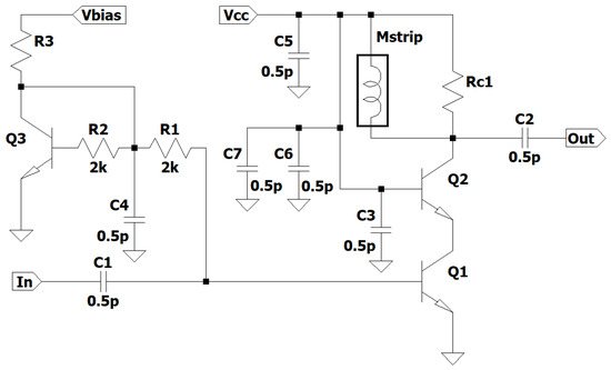
Figure 3.
Schematic of the single-stage LNA core.
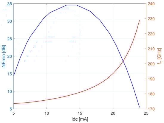
Figure 4.
Transition frequency (red curve) and minimum Noise Figure (blue curve) of the 2-finger 4 μm device as a function of the bias current.
The relatively low fractional bandwidth (below 15% in both cases) enabled the use of single-stub matching networks. Microstrip lines provided by the technological process were employed to transform Rin and Rout to 50 Ω. The negative susceptive component at the input was compensated by means of a shunt capacitor to ground. At the output, where the resulting susceptance was positive, a narrow microstrip line short-circuited to ground was used to emulate the required tuning inductance. The simulated gain of the complete two-stage LNA was 18 dB for the low-band design and 14 dB for the high-band design. For both amplifiers, the simulated Noise Figure remained below 8 dB across the entire specified bandwidth. To assess design robustness, PVT analyses were performed by considering multiple process corners for HBTs and resistors, together with supply–voltage variations (±5%) and temperature variations in the range of 0–70 °C. Post-layout simulation results for the low-band LNA at 140 GHz are reported in Table 1. The most significant performance variation is attributed to temperature. In particular, since the HBT bias current decreases as temperature increases, the adoption of a PTAT (proportional-to-absolute-temperature) bias circuit could mitigate the sensitivity of the amplifier to temperature variations.

Table 1.
Post-layout low-band LNA performance at 140 GHz under PVT variation.
3.2. Design of D-Band-to-E-Band Down-Converter
For each of the two sub-bands, a down-conversion mixer from the D-band to the E-band was designed in order to form, together with the corresponding LNA, a complete down-conversion front-end. An initial mixer implementation was developed using a two-quadrant multiplier architecture and E-band passive baluns, as shown in Figure 5. The same 4 μm, two-finger HBT device selected for the LNA design was adopted for the transconductor stage, whereas 2 μm, two-finger devices were employed in the switching stage. In the transconductor stage, inductive emitter degeneration was introduced to improve linearity and optimize the overall performance. A bias current of 13 mA was selected for the transconductor, since, in this case, conversion gain is a more critical design parameter than the Noise Figure. The second step of the proposed design flow was then applied by defining a composite device comprising the transconductor, the emitter degeneration inductor, and the switching stage. The corresponding single-frequency model was extracted for different values of the degeneration inductance in order to evaluate its impact on the small-signal parameters and to identify the optimal design trade-off.
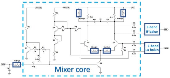
Figure 5.
Schematic of the down-conversion mixer.
In this case, a collector capacitance CC was introduced in the tuned load in order to limit the required value of LC and, consequently, to reduce the corresponding microstrip length at the collector node, thereby preventing self-resonance phenomena. A single-stub matching network was designed at the D-band input.
The simulated conversion gain for both the low-band and high-band mixers is reported in Figure 6. The simulated input 1 dB compression point is −7.6 dBm at 140 GHz for the low-band mixer and −6.6 dBm at 157.5 GHz for the high-band mixer.
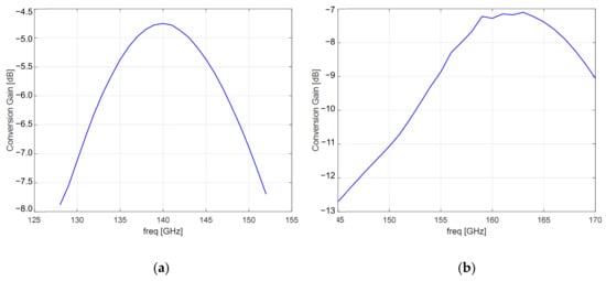
Figure 6.
Simulated conversion gain of the low-band (130–150 GHz RF input) (a) and high-band (150–165 GHz RF input) (b) mixers.
4. Measurement Results and Discussion
Two chips, one containing the stand-alone LNA and the other integrating the complete D-band-to-E-band down-converter, were fabricated in 55 nm SiGe BiCMOS technology [6] developed by STMicroelectronics, featuring fT = 385 GHz and fMAX = 500 GHz. Each chip includes both the low-band and high-band implementations of the designed circuits. The die area is 1 mm × 1 mm. The adopted technology provides high-speed HBTs, low-loss microstrip transmission lines, and high-quality-factor (high-Q) RF inductors and capacitors. The capacitors used in the LNA design are integrated metal–oxide–metal (MOM) capacitors available in the PDK. According to PDK specifications and EM-assisted simulations, the quality factor Q of these capacitors ranges approximately from 20 to 40 within the D-band frequency range (130–165 GHz), depending on the capacitance value and layout configuration. To supply the DC bias voltages, the dies were mounted and wire-bonded onto a dedicated test board designed at the University of Rome. Circuit characterization was performed at the laboratories of University of Rome Tor Vergata using D-band ground–signal–ground (GSG) probes.
For each sub-band, the two-stage LNA was characterized in terms of S-parameters using a probe station. Figure 7 shows the microphotograph of the LNA die during the S-parameter measurements. The measured S-parameters of the low-band and high-band LNAs are reported in Figure 8 and Figure 9, respectively. In both cases, a measured gain exceeding 13 dB was achieved, with a −3 dB bandwidth of approximately 14 GHz. However, a downward shift in the center frequency was observed for both designs. In particular, the shift amounts to approximately 14.5 GHz (11%) for the low-band LNA (see the comparison in Figure 9) and 20 GHz (16%) for the high-band LNA (see Figure 10). The simulated NF is also included in the corresponding figures for comparison.
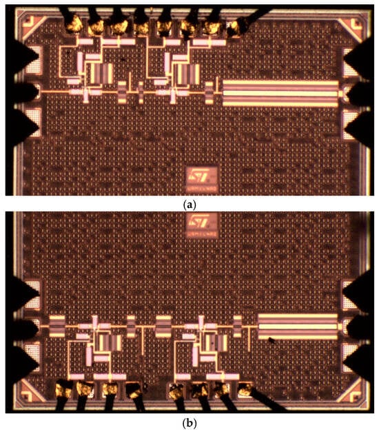
Figure 7.
Micro-photograph of the two sections of the chip (1 mm × 1 mm die size) showing the high-band (a) and the low-band (b) LNAs during measurements by D-band GSG probes.
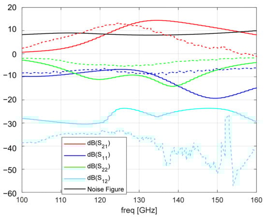
Figure 8.
Comparison of measured (dot lines) and simulated (solid lines) performance of the low-band LNA and simulated Noise Figure.
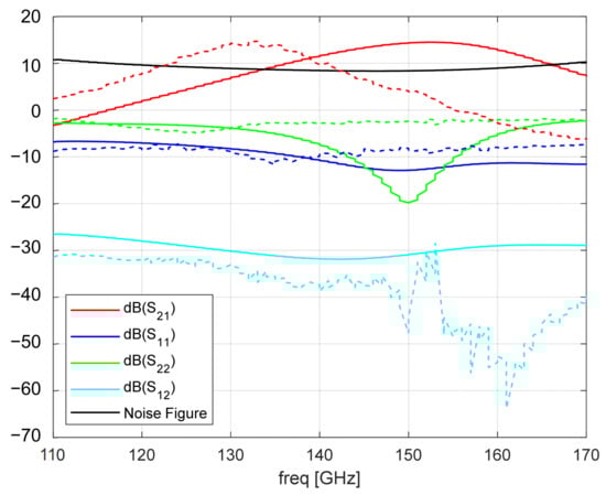
Figure 9.
Comparison of measured (dot lines) and simulated (solid lines) performance of the high-band LNA and simulated Noise Figure.
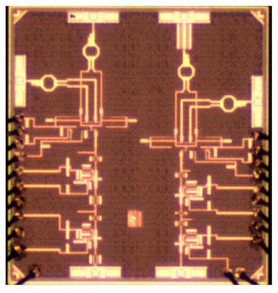
Figure 10.
Micro-photograph of the chip (die size 1.4 mm × 1.3 mm) hosting the two downconverters bonded to the test board.
A detailed analysis of the measurement results indicates that the parasitic elements of the HBTs were underestimated during the design phase. This underestimation led to a frequency downshift of the LNA bandwidth, with the effect becoming more pronounced as the carrier frequency increases.
The die area of the chip integrating the two down-converters is 1.4 mm × 1.3 mm. For both sub-bands, a preliminary characterization of the fabricated down-converters (shown in Figure 10) was carried out in terms of conversion gain, using a spectrum analyzer connected to the intermediate-frequency (IF) port. An external ×3 E-band (60–90 GHz) frequency multiplier was employed to generate the local oscillator (LO) signal from a K-band signal generator. A photograph of the measurement setup is provided in Figure 11. Figure 12 reports the measured conversion gain in the E-band for an LO frequency of fLO = 60 GHz, obtained from two different low-band front-end down-converter boards.
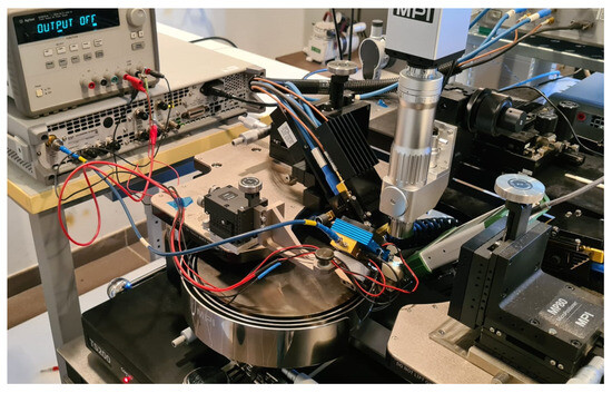
Figure 11.
Lab setup for conversion gain measurement.
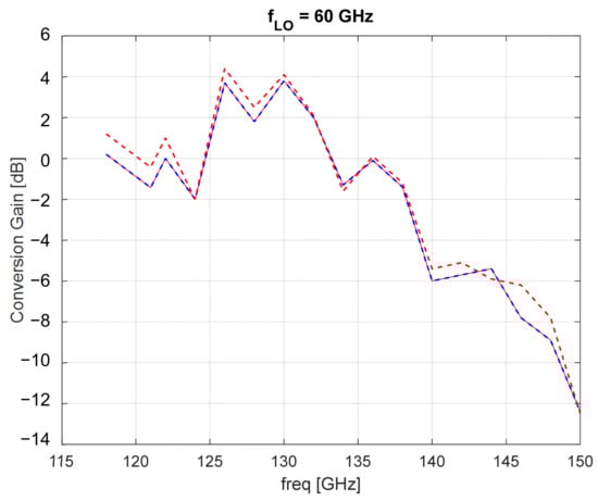
Figure 12.
Measured conversion gain of two different low-band down-converter boards.
As can be observed, the measured performance is highly repeatable across the two boards. Nevertheless, a significant reduction in conversion gain is observed compared to the simulated results.
In Figure 13, the measured conversion gain of the high-band down-converter at fLO = 65 GHz is reported, once again showing a significant reduction compared to the simulated results. Based on the measured down-converter conversion gain (approximately +4 dB) and the measured LNA gain (approximately +14 dB), the stand-alone mixer conversion loss can be estimated to be about 10 dB. This value is approximately 3 dB (5 dB) lower than the simulated value shown in Figure 6 for the high-band (low-band) mixer.
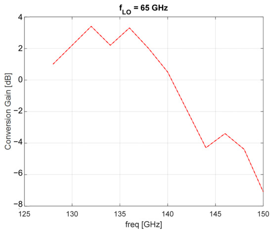
Figure 13.
Measured conversion gain of a high-band down-converter board.
Further analysis is required to determine whether the downward shift in the center frequency is the only factor responsible for the gain degradation (the previously measured LNAs correspond to the first stage of the down-converter). Another possible explanation is that insufficient LO power is delivered to the circuit, since 60 GHz lies outside the LO port bandwidth. Moreover, the frequency multiplier used has a minimum operating frequency of 60 GHz; however, a lower frequency would be required to compensate for the RF input downshift.
5. Conclusions and Future Work
A comprehensive design methodology for the receiver blocks of a D-band receiver has been proposed and validated through the design, prototyping, and characterization of two-stage LNAs and D-band-to-E-band downconverters consisting of an LNA followed by a mixer. Two different circuit pairs were designed to operate at center frequencies of 140 GHz and 157.5 GHz, respectively, in order to cover the 130–165 GHz band. Experimental results confirmed the validity of the proposed approach and emphasized the importance of accurate parasitic extraction for both active and passive devices, as a downward shift in the center frequency was observed. To address this issue, a more accurate parasitic extraction procedure was implemented, and a new set of circuits was designed and prototyped to provide further validation of the proposed methodology in future work.
Author Contributions
Conceptualization, P.T. and A.T.; methodology, G.D.F., L.P., A.M. and P.T.; software, H.S. and P.T.; validation, H.S.; formal analysis, P.T. and A.T.; investigation, G.D.F., A.M. and L.P.; resources, A.T.; data curation, P.T. and H.S.; writing—original draft preparation, P.T. and A.T.; writing—review and editing, G.D.F., L.P. and P.T.; visualization, H.S. and A.T.; supervision, A.T.; project administration, A.T.; funding acquisition, A.T. All authors have read and agreed to the published version of the manuscript.
Funding
This work was supported by the Commission of the European Union under the HORIZON-KDT-JU grant SHIFT “Sustainable tecHnologies enablIng Future Telecommunication applications”, no. 101096256.
Data Availability Statement
The raw data supporting the conclusions of this article will be made available by the authors upon request.
Acknowledgments
The authors wish to thank the research team of E. Limiti at Roma Tor Vergata University for S-parameters and conversion gain measurements carried out in their labs.
Conflicts of Interest
The authors declare no conflicts of interest.
References
- Amendola, G.; Boccia, L.; Centurelli, F.; Chevalier, P.; Fonte, A.; Karman, S.; Levantino, S.; Mazzanti, A.; Mustacchio, C.; Pallotta, A.; et al. SiGe BiCMOS building blocks for E-and D-band backhauling front-ends. In Proceedings of the 2021 16th European Microwave Integrated Circuits Conference (EuMIC), London, UK, 3–4 April 2022; pp. 113–116. [Google Scholar]
- Frecassetti, M.G.; Mazzanti, A.; Sevillano, J.F.; Del Rio, D.; Ermolov, V. D-band transport solution to 5G and beyond 5G cellular networks. In Proceedings of the 2019 European Conference on Networks and Communications (EuCNC), Valencia, Spain, 18–21 June 2019; pp. 214–218. [Google Scholar]
- Maiwald, T.; Li, T.; Hotopan, G.R.; Kolb, K.; Disch, K.; Potschka, J.; Haag, A.; Dietz, M.; Debaillie, B.; Zwick, T.; et al. A review of integrated systems and components for 6G wireless communication in the D-band. Proc. IEEE 2023, 111, 220–256. [Google Scholar] [CrossRef]
- del Rio, D.; Sevillano, J.F.; Torres, R.; Irizar, A.; Roux, P.; Pirbazari, M.M.; Mazzanti, A.; Säily, J.; Lamminen, A.; de Cos, J.; et al. A D-band 16-element phased-array transceiver in 55-nm BiCMOS. IEEE Trans. Microw. Theory Tech. 2022, 71, 854–869. [Google Scholar] [CrossRef]
- Heinemann, B.; Rücker, H.; Barth, R.; Bärwolf, F.; Drews, J.; Fischer, G.G.; Fox, A.; Fursenko, O.; Grabolla, T.; Herzel, F.; et al. SiGe HBT with fx/fmax of 505 GHz/720 GHz. In Proceedings of the 2016 IEEE International Electron Devices Meeting (IEDM), San Francisco, CA, USA, 3–7 December 2016; pp. 3.1.1–3.1.4. [Google Scholar]
- Chevalier, P.; Cacho, F.; Durand, C.; Derrier, N.; Milon, V.; Monsieur, F.; Gauthier, A.; Billy, P.; Fregonese, S.; Zimmer, T.; et al. A Versatile 55-nm SiGe BiCMOS Technology for Wired, Wireless, and Satcom Applications. In Proceedings of the 2024 IEEE BiCMOS and Compound Semiconductor Integrated Circuits and Technology Symposium (BCICTS), Fort Lauderdale, FL, USA, 27–30 October 2024; pp. 13–17. [Google Scholar]
- Böck, J.; Aufinger, K.; Knapp, H.; Mukherjee, A.; Wohlmuth, H.D.; Komenko, V.; Rothenhäußer, S.; Tschumakow, D.; Stavrev, M. 530GHz fmax 90nm SiGe BiCMOS Technology for Sensing and Communication Applications. In Proceedings of the 2025 16th German Microwave Conference (GeMiC), Dresden, Germany, 17–19 March 2025; pp. 358–361. [Google Scholar]
- Hou, D.; Xiong, Y.Z.; Goh, W.L.; Hong, W.; Madihian, M. A D-band cascode amplifier with 24.3 dB gain and 7.7 dBm output power in 0.13μm SiGe BiCMOS technology. IEEE Microw. Wirel. Compon. Lett. 2012, 22, 191–193. [Google Scholar]
- Fritsche, D.; Carta, C.; Ellinger, F. A Broadband 200 GHz Amplifier with 17 dB Gain and 18 mW DC-Power Consumption in 0.13 μm SiGe BiCMOS. IEEE Microw. Wirel. Compon. Lett. 2014, 24, 790–792. [Google Scholar] [CrossRef]
- Ulusoy, A.Ç.; Song, P.; Khan, W.T.; Kaynak, M.; Tillack, B.; Papapolymerou, J.; Cressler, J.D. A SiGe D-band low-noise amplifier utilizing gain-boosting technique. IEEE Microw. Wirel. Compon. Lett. 2015, 25, 61–63. [Google Scholar] [CrossRef]
- Aguilar, E.; Hagelauer, A.; Kissinger, D.; Weigel, R. A low-power wideband D-band LNA in a 130 nm BiCMOS technology for imaging applications. In Proceedings of the 2018 IEEE 18th Topical Meeting on Silicon Monolithic Integrated Circuits in RF Systems (SiRF), Anaheim, CA, USA, 14–17 January 2018; pp. 27–29. [Google Scholar]
- Ustundag, B.; Turkmen, E.; Cetindogan, B.; Guner, A.; Kaynak, M.; Gurbuz, Y. Low-noise amplifiers for W-band and D-band passive imaging systems in SiGe BiCMOS technology. In Proceedings of the 2018 Asia-Pacific Microwave Conference (APMC), Kyoto, Japan, 6–9 November 2018; pp. 651–653. [Google Scholar]
- Turkmen, E.; Cetindogan, B.; Yazici, M.; Gurbuz, Y. Design and characterization of a D-band SiGe HBT front-end for Dicke radiometers. IEEE Sens. J. 2020, 20, 4694–4703. [Google Scholar] [CrossRef]
- Petricli, I.; Lotfi, H.; Mazzanti, A. Analysis and design of D-band cascode SiGe BiCMOS amplifiers with gain-bandwidth product enhanced by load reflection. IEEE Trans. Microw. Theory Tech. 2021, 69, 4059–4068. [Google Scholar] [CrossRef]
- Andree, M.; Grzyb, J.; Heinemann, B.; Pfeiffer, U. A D-band to J-band low-noise amplifier with high gain-bandwidth product in an advanced 130 nm SiGe BiCMOS technology. In Proceedings of the 2023 IEEE Radio Frequency Integrated Circuits Symposium (RFIC), San Diego, CA, USA, 11–13 June 2023; pp. 137–140. [Google Scholar]
- Maiwald, T.; Potschka, J.; Kolb, K.; Dietz, M.; Aufinger, K.; Visweswaran, A.; Weigel, R. A full D-band low noise amplifier in 130 nm SiGe BiCMOS using zero-ohm transmission lines. In Proceedings of the 2020 15th European Microwave Integrated Circuits Conference (EuMIC), Utrecht, The Netherlands, 10–15 January 2021; pp. 13–16. [Google Scholar]
- Moradinia, A.; Rao, S.G.; Cressler, J.D. A SiGe HBT D-band LNA utilizing asymmetric broadside coupled lines. IEEE Microw. Wirel. Technol. Lett. 2023, 33, 707–710. [Google Scholar] [CrossRef]
- Urain, A.; del Rio, D.; Beriain, A.; Solar, H. Area-Efficient SiGe BiCMOS LNA with Wideband Frequency Tuning Capability Across D and G Bands. IEEE Trans. Circuits Syst. I Regul. Pap. 2025, 72, 1114–1125. [Google Scholar] [CrossRef]
- Roux, P.; Singh, A.; Jorge, F.; Moretto, M.; Baeyens, Y. Wideband variable gain amplifier for D-band Backhaul Transceiver in 55 nm BiCMOS Technology. In Proceedings of the 2019 IEEE Asia-Pacific Microwave Conference (APMC), Singapore, 10–13 December 2019; pp. 1313–1315. [Google Scholar]
- Karakuzulu, A.; Eissa, M.H.; Kissinger, D.; Malignaggi, A. Full D-band transmit–receive module for phased array systems in 130-nm SiGe BiCMOS. IEEE Solid-State Circuits Lett. 2021, 4, 40–43. [Google Scholar] [CrossRef]
- Ahmed, F.; Furqan, M.; Heinemann, B.; Stelzer, A. A SiGe-based broadband 140–170-GHz downconverter for high resolution FMCW radar applications. In Proceedings of the 2016 IEEE MTT-S International Conference on Microwaves for Intelligent Mobility (ICMIM), San Diego, CA, USA, 19–20 May 2016; pp. 1–4. [Google Scholar]
- Fritsche, D.; Tretter, G.; Stärke, P.; Carta, C.; Ellinger, F. A low-power SiGe BiCMOS 190-GHz receiver with 47-dB conversion gain and 11-dB noise figure for ultralarge-bandwidth applications. IEEE Trans. Microw. Theory Tech. 2017, 65, 4002–4013. [Google Scholar] [CrossRef]
- Stärke, P.; Seidel, A.; Carta, C.; Ellinger, F. Direct-conversion receiver front-end for 180 GHz with 80 GHz bandwidth in 130 nm SiGe. In Proceedings of the 2019 IEEE Asian Solid-State Circuits Conference (A-SSCC), Macao, China, 4–6 November 2019; pp. 161–164. [Google Scholar]
- Maiwald, T.; Potschka, J.; Kolb, K.; Dietz, M.; Hagelauer, A.; Visweswaran, A.; Weigel, R. A broadband zero-IF down-conversion mixer in 130 nm SiGe BiCMOS for beyond 5G communication systems in D-band. IEEE Trans. Circuits Syst. II Express Briefs 2021, 68, 2277–2281. [Google Scholar] [CrossRef]
- Luo, X.; Zhou, W.; Cheng, X.; Rao, Y.; Han, C.; Han, J.; Zhang, L.; Cheng, B.; Deng, X. A D-band down-conversion gilbert mixer based on electromagnetic coupling gain-boosted topology in 130 nm SiGe BiCMOS. Analog Integr. Circuits Signal Process. 2025, 123, 38. [Google Scholar] [CrossRef]
- Abbassi, F.; Aziri, S.; Abbas, W.; Wagner, C.; Aufinger, K.; Ostermann, T. A D-Band Active Down-Conversion Mixer with 80 GHz IF for FMCW Radar Frequency Extension. In Proceedings of the 2025 Austrochip Workshop on Microelectronics (Austrochip), Linz, Austria, 24–25 September 2025; pp. 29–32. [Google Scholar]
- Petricli, I.; Riccardi, D.; Mazzanti, A. D-Band SiGe BiCMOS Power Amplifier With 16.8 dBm P1dB and 17.1% PAE Enhanced by Current-Clamping in Multiple Common-Base Stages. IEEE Microw. Wirel. Compon. Lett. 2021, 31, 288–291. [Google Scholar] [CrossRef]


Disclaimer/Publisher’s Note: The statements, opinions and data contained in all publications are solely those of the individual author(s) and contributor(s) and not of MDPI and/or the editor(s). MDPI and/or the editor(s) disclaim responsibility for any injury to people or property resulting from any ideas, methods, instructions or products referred to in the content. |
© 2026 by the authors. Licensee MDPI, Basel, Switzerland. This article is an open access article distributed under the terms and conditions of the Creative Commons Attribution (CC BY) license.