Abstract
This study introduces a rectenna, functioning as an RF envelope detector, utilizing a 16 nm bulk MOS transistor (metal-oxide-semiconductor field-effect transistor) for nonlinear detection. A circuit architecture is presented alongside a detailed design methodology and simulations. The detector efficiently demodulates a 2.4 GHz OOK (On/Off Keying) encoded signal, comprising a 32-bit word, within 320 μs. Remarkably, the circuit operates passively, requiring no voltage supply or bias current, and functions effectively with dBm input power at the antenna. This capability enables the decoding of 32-bit unsigned integer radio packets as a wakeup radio event. The effectiveness of the envelope detector is substantiated through comprehensive simulations.
1. Introduction
Wireless sensor networks (WSNs) and IoT edge-nodes are pivotal in developing long-lasting, low-energy applications, ideally functioning without maintenance. Given the reliance on batteries or energy harvested from the environment, maximizing the operational lifespan is crucial. In WSNs and IoT edge-nodes, the energy consumption for network communication predominates over other tasks like managing node hardware resources (e.g., sensors and microcontrollers). Consequently, a major research focus in WSN and IoT applications is the minimization of unnecessary communication while maintaining network efficacy. To reduce energy expenditure in wireless communication, two techniques are employed: (i) duty-cycle protocols, where the transceiver is active for a set percentage of time, and (ii) radio event-triggered receivers using ultra-low-power wakeup circuits or rectennas.
While the former method is prevalent due to the ready availability of IEEE 802.15.4-compliant radio transceivers (such as the radio transceiver CC2420 or the CC2538 system-on-chip (SoC) with an integrated ARM Cortex-M3-based microcontroller), it typically operates at the software level, fostering short duty cycles to conserve energy.
Consequently, the transceiver spends most of its time in deep sleep mode, significantly reducing battery current consumption (to the order of μA), and activates only to acknowledge communication or relay packets. Several techniques are proposed in the literature to optimize the transceiver’s duty cycle, focusing on how nodes can awaken solely for net synchronization or packet transmission to adjacent nodes. The duty-cycle method has faced criticism due to its significant increase in microcontroller computational load and memory usage. Consequently, many WSN designers are shifting toward the event-triggered radio approach. This method involves nodes equipped with an auxiliary receiver (WuRx (wakeup-receiver) or rectenna) that continuously monitors the radio channel with minimal battery consumption. This receiver can detect specific signal patterns from a remote node attempting communication, triggering the activation of the main radio transceiver and the node itself.
A wakeup receiver (or rectenna) offers substantial advantages over the sleep/wakeup duty-cycle method in terms of both power dissipation and latency. This is further elaborated in [1], which includes a comprehensive state-of-the-art survey.
Comparing our approach with the state of the art is essential. We refer to Table 1, updated from our previous work [2], to address two points: (i) the need to clarify our definition of “sensitivity”, as the term is interpreted differently in the literature (either as voltage surpassing a certain threshold or BER (bit error rate) exceeding a specific threshold), and (ii) the absence of a mature technology for constructing rectennas, with options including diodes or MOS transistors.
Regarding our previous work [2], we will mention here that there are significant differences. In this case study, we use a MOS transistor with zero bias and the bulk connected to the source as the nonlinear detecting element, instead of a biased diode. Moreover, this novel simple rectenna does not require a voltage power supply.
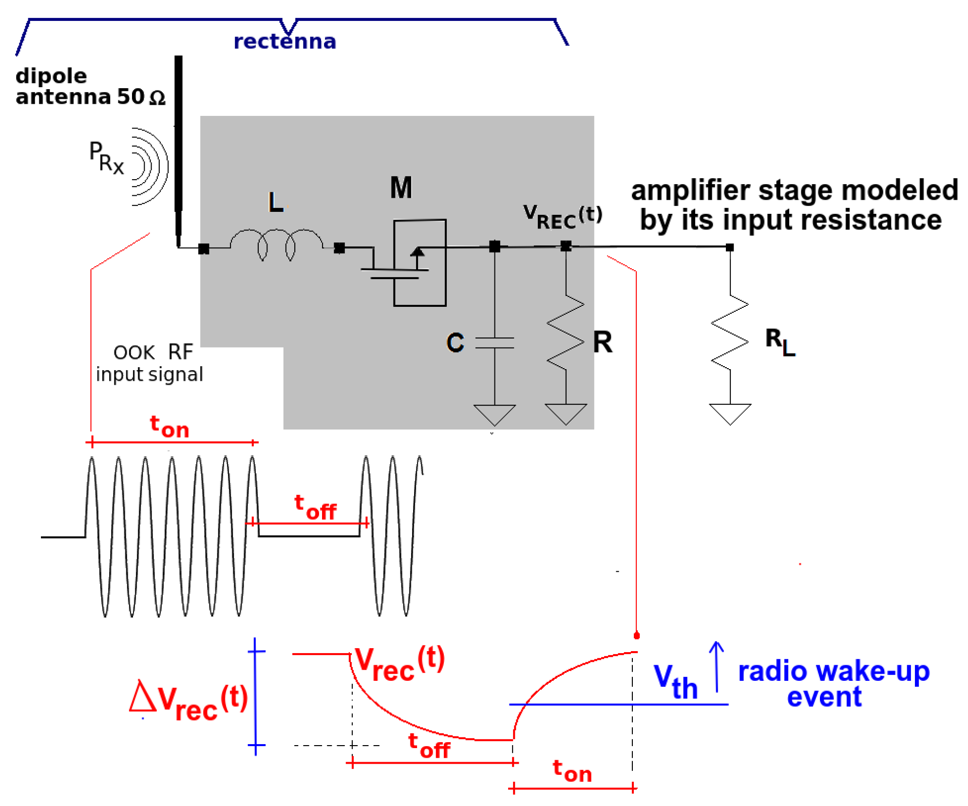
For “sensitivity”, we define it as the minimum antenna input power required to induce a bit switch in the subsequent rectenna back-end circuit, such as a comparator or latch (Figure 1; modeled by ). It can be implemented, for example, by optimizing certain circuits architectures, as shown in [3].
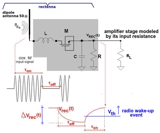
Figure 1.
Proposed rectenna architecture.
Table 1 presents a performance comparison with other publications, providing references for wakeup circuit design methods and technological alternatives.

Table 1.
Summary and comparison of WuRx receiver front-end performance with state-of-the-art technologies (updated from [2]).
Table 1.
Summary and comparison of WuRx receiver front-end performance with state-of-the-art technologies (updated from [2]).
| Reference | Band (MHz) | Minimum (dBm) for a Reliable Wakeup Event (1) | Reliable Wakeup Event Criterion | Data Rate (), Modulation Scheme | Reported Power Consumption | Rectenna Technology | Load Resistance () for Amplification |
|---|---|---|---|---|---|---|---|
| [2] | 2450 | −54.7 | when | 3.276, OOK | 0.98 μA | one diode | assumed infinite |
| [4] | 868 | −55 | 10, OOK | 0 (2) | diodes | N/A | |
| [5] | 2000 | −72 | when | 40 typical, OOK | 52 μW (3) | 90 nm CMOS | N/A |
| [6] | 2400/915 | −75/−64 | when dB (4) | 100, OOK | 51 μW (4) | 90 nm CMOS | N/A |
| [7] | 2400/5800 | −65/−50 | when dB (5) | 100, OOK | 1.5 μW (5) | 180 nm CMOS | N/A |
| [8] | 2400 | −50 | when | 100, OOK | 2.4 μW (6) | 180 nm CMOS | N/A |
| [9] | 2400/915 | −43.4/−43.2 | when | 12.5, OOK (7) | 0 (7) | 130 nm CMOS | N/A |
| [10] | 2450/868 | −45.2/−53.4 | (8) | 10, OOK | 0 (8) | diodes | N/A |
| This work | 2450 | −53 | 100, OOK | 0, passive | 16 nm CMOS | 500 M |
(1) RF OOK (On/Off Keying) input power signal, referred to as wakeup sensitivity. (2) Total circuit power consumption 196 nW in idle listening. is the offset voltage of comparators, e.g., with LPV7215 mV. (3) Prototype uses RF-MEMS resonators; voltage power supply at 0.5 V; rectenna power consumption in idle listening. (4) Total circuit power consumption when in idle listening; rectenna consumption is not separately reported. Final WuRx output SNR. (5) Envelope detector (rectenna) power consumption in idle listening. Final WuRx output SNR. (6) The rectenna power consumption is 2.4 μW; the total circuit current consumption is 4.5 μA in idle listening. (7) The rectenna comprises a 30-stage ZVT MOS transistor as diode rectifier; 116 nW total circuit power in idle listening. (8) Total circuit power consumption 1.276 μW in idle listening; the rectenna functions as a voltage doubler. Threshold mV.
In this study, we evaluate a design based on a 16 nm MOS transistor, with zero bias and with the bulk connected to the source as the nonlinear detecting element. This choice is due to the widespread use of MOS transistors in GHz rectenna designs. We note that the recent literature on this topic often lacks a mathematical analysis of the nonlinear behavior of MOS transistors under zero-bias currents and 2.45 GHz signals. This is because there are no closed equations to model the nonlinear elements of the rectenna, and for this reason, we overcome the problem using simulations.
Therefore, formal simulations are crucial for advancing the performance beyond the current state of the art, which is a primary focus of this work. This includes the innovative use of a MOS transistor configuration, along with the matching and load networks. The authors are specifically focused on the rectenna design, aiming to achieve the following: (i) low cost, (ii) minimal components, (iii) compatibility with standard IEEE 802.15.4-compliant WSNs operating in the 2.4 GHz band, and (iv) operation without a voltage supply (passive).
2. Rectenna Design Criterion and Simulations
Figure 1 illustrates the rectenna, comprising the following components: (i) antenna, (ii) inductance L for impedance matching, (iii) envelope detector (consisting of a MOS transistor with capacitance and resistance), and (iv) amplifier stage, modeled by its input resistance (back-end, responsible for decision-making functionality). Detection is facilitated by the nonlinear current–voltage (I–V) characteristic in the MOS junctions. The antenna receives an OOK encoded signal at a carrier frequency of 2.45 GHz, with the involved times, (receiving bit “1”) and (receiving bit “0”), determining the baud rate.
It is important to note that most 802.15.4-compliant radio transceivers have a test mode, allowing the wireless sensor node to perform OOK transmissions solely for testing purposes. This capability is sufficient for implementing the OOK rectenna. However, most studies in the literature, including works such as [8], do not detail the generation of the OOK signal, and so generally, the rectennas in Table 1 are tested using a signal generator rather than a real antenna receiving signals or using accurate simulations of the antenna, as performed in this work.
Let represent the voltage level difference between bits ‘0’ and ‘1’. The design aims to determine the optimal set (W is the transistor width) for a given load , maximizing and the baud rate, using a zero-bias bulk-source connected MOS transistor without a voltage power supply. This multi-objective optimization framework can be simplified into a single-objective approach, given the minimal circuit design and the use of LTspice simulations. In particular, the .STEP command in LTspice simulator facilitates the repeated execution of a transient .TRAN analysis while adjusting global parameters, looking for performance corners. These steps can be linear or specified as a list of values, enabling the efficient exploration of the unknown circuit elements to identify the best values for achieving the maximum at the highest baud rate.
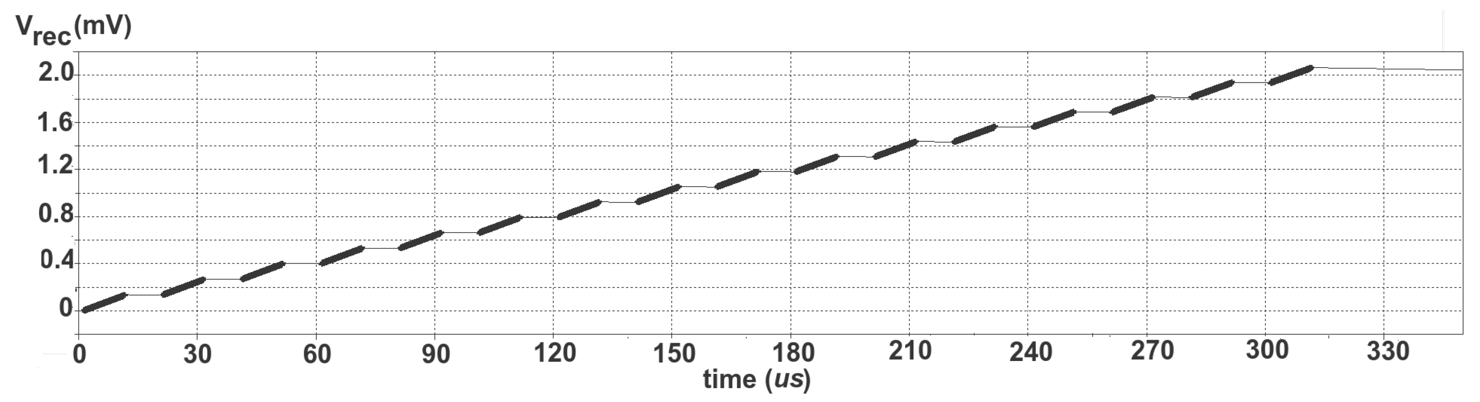
After several iterations, an optimal design is achieved with the following: nH, pF, M and nm; this results in mV at μs (see Figure 2). The input resistance of the subsequent amplification stage (assumed to be infinite) could be designed using MOSFET technology with capacitive input impedance. Notably, this straightforward design method relies on simulation, bypassing the need for a qualitative analysis of the RF signal’s contribution through the MOSFET to the output or complex equations to model the rectenna.
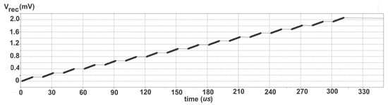
Figure 2.
A 32-bit signal detected at the receiver when reaches 2 mV (by transmitting a 32-bit unsigned integer). The preceding circuitry can trigger an event by amplifying the signal or using a latch to wake up the radio of the wireless sensor node.
We would like to highlight that our initial optimization, using the .STEP transitory analysis in LTspice, employs lumped components and does not account for package parasitics. Following this preliminary stage, we refine our solution by incorporating comprehensive LTspice models to accurately estimate the achievable performance.
Additionally, we take into account the perimeter of the MOS transistor to evaluate the extrinsic parasitic capacitances. A section of the LTspice netlist for this configuration is as follows (Listing 1):
| Listing 1. A relevant section of the LTspice code. |
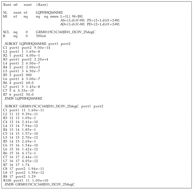 |
Consequently, our simulations and reports include the following components: The inductor L is an RF Inductor from Murata Manufacturing Co., Ltd., Kyoto, Japan, part number LQP03HQ16NH02, size code inch 0201, 16 nH inductance with a 3% tolerance, a self-resonance frequency of GHz, a current rating of 250 mA (SPICE model: [11]). The capacitor C is sourced from Murata Manufacturing Co., Ltd. part number GRM0115C1C160JE01, measuring 0.25 mm × 0.125 mm × 0.125 mm, with a capacitance of 16 pF and a 5% tolerance (SPICE model: [12]). The MOS transistor is based on the PTM Low-Power 16 nm Metal Gate, High-K, Strained-Si SPICE model level 54 (bsim4) [13].
The drain impedance of the MOS transistor is influenced by the received power , but from our experience, it remains approximately constant for values less than −15 dBm. This assumption is applicable to the current work, considering the maximum transmission power of the node () is 0 dBm, and in WSN applications, the received power is often significantly lower due to radio channel attenuation.
In our circuit model, replacing the antenna, we use an equivalent comprising a resistance and a series-connected voltage power supply V, representing the Thevenin equivalent circuit of the antenna. The maximum input power delivered to the load by the antenna is expressed as , assuming conjugate matching conditions. For our optimization method (maximizing using the .STEP command), we set V = 1mV, corresponding to a radio frequency input power of −53 dBm. This value is selected as the target minimum input power for our case study. The final result is depicted in Figure 2.
3. Conclusions
Wakeup receivers, or rectennas, present novel avenues for energy-efficient communication in WSNs. We have designed a rectenna based on a simple, minimal topology, employing a MOS transistor as the nonlinear detecting element. This transistor is uniquely configured with its bulk connected to the source and operated at zero bias, differing from traditional MOS configurations.
Our results demonstrate the feasibility of deploying such a solution in wireless sensor nodes.
Through simulations, we have verified that the optimal set of design parameters , including the transistor size, maximizes the . This optimization is achieved using a straightforward LTspice command to vary parameters in transient simulations.
The sensitivity and simplified circuitry of our rectenna design outperform those of the design proposed in [9] and other MOS transistor-based designs, as shown in Table 1.
Funding
This research received no external funding.
Institutional Review Board Statement
Not applicable.
Informed Consent Statement
Not applicable.
Data Availability Statement
Circuit netlist and code for simulations are available upon request.
Conflicts of Interest
The authors declare no conflicts of interest.
References
- Demirkol, I.; Ersoy, C.; Onur, E. Wake-Up Receivers for Wireless Sensor Networks: Benefits and Challenges. IEEE Wirel. Commun. 2009, 16, 88–96. [Google Scholar] [CrossRef]
- Siniscalchi, M.; Pieruccioni, A.; Vanzini, F.; Reyes, L.; Barboni, L. Schottky Diode Assessment for Implementing a Rectenna for Radio-Triggered Wireless Sensor Networks. IEEE Microw. Wirel. Components Lett. 2017, 27, 763–765. [Google Scholar] [CrossRef]
- Ramkaj, A.; Steyaert, M.; Tavernier, F. A 13.5-Gb/s 5-mV-Sensitivity 26.8-ps-CLK–OUT Delay Triple-Latch Feedforward Dynamic Comparator in 28-nm CMOS. IEEE Solid-State Circuits Lett. 2019, 2, 167–170. [Google Scholar] [CrossRef]
- Magno, M.; Benini, L. An ultra low power high sensitivity wake-up radio receiver with addressing capability. In Proceedings of the 2014 IEEE 10th International Conference on Wireless and Mobile Computing, Networking and Communications (WiMob), Larnaca, Cyprus, 8–10 October 2014; pp. 92–99. [Google Scholar] [CrossRef]
- Pletcher, N.; Rabaey, J. Ultra-Low Power Wake-Up Receiver for Wireless Sensor Networks. Ph.D. Thesis, EECS Department, University of California, Berkeley, CA, USA, 2008. [Google Scholar]
- Huang, X.; Rampu, S.; Wang, X.; Dolmans, G.; de Groot, H. A 2.4 GHz/915 MHz 51 μW wake-up receiver with offset and noise suppression. In Proceedings of the IEEE International Solid-State Circuits Conference—(ISSCC), San Francisco, CA, USA, 7–11 February 2010; pp. 222–223. [Google Scholar] [CrossRef]
- Cheng, K.; Liu, X.; Je, M. A 2.4/5.8 GHz 10 uW Wake-Up Receiver with -65/-50 dBm Sensitivity Using Direct Active RF Detection. In Proceedings of the IEEE Asian Solid-State Circuits Conference, Kobe, Japan, 12–14 November 2012. [Google Scholar]
- Chen, S.; Yang, C.; Cheng, K. A 4.5 uW 2.4 GHz wake up receiver based on complementary current reuse RF detector. In Proceedings of the 2015 IEEE International Symposium on Circuits and Systems (ISCAS), Lisbon, Portugal, 24–27 May 2015; pp. 1214–1217. [Google Scholar] [CrossRef]
- Seunghyun, O.; Roberts, N.; Wentzloff, D. A 116nW multi-band wake-up receiver with 31-bit correlator and interference rejection. In Proceedings of the IEEE 2013 Custom Integrated Circuits Conference, San Jose, CA, USA, 22–25 September 2013; pp. 1–4. [Google Scholar] [CrossRef]
- Prete, M.D.; Masotti, D.; Costanzo, A.; Magno, M.; Benini, L. A 2.4 GHz-868 MHz dual-band wake-up radio for wireless sensor network and IoT. In Proceedings of the 2015 IEEE 11th International Conference on Wireless and Mobile Computing, Networking and Communications (WiMob), Abu Dhabi, United Arab Emirates, 19–21 October 2015; pp. 322–328. [Google Scholar] [CrossRef]
- Murata Manufacturing Co., Ltd. MURATA P/N GRM0115C1C160JE01; Murata Manufacturing Co., Ltd.: Kyoto, Japan, 2023. [Google Scholar]
- Murata Manufacturing Co., Ltd. MURATA P/N LQP03HQ16NH02; Murata Manufacturing Co., Ltd.: Kyoto, Japan, 2023. [Google Scholar]
- Predictive Technology Model Level 54. In PTM LP Model. Available online: https://mec.umn.edu/ptm (accessed on 30 June 2024).
Disclaimer/Publisher’s Note: The statements, opinions and data contained in all publications are solely those of the individual author(s) and contributor(s) and not of MDPI and/or the editor(s). MDPI and/or the editor(s) disclaim responsibility for any injury to people or property resulting from any ideas, methods, instructions or products referred to in the content. |
© 2024 by the author. Licensee MDPI, Basel, Switzerland. This article is an open access article distributed under the terms and conditions of the Creative Commons Attribution (CC BY) license (https://creativecommons.org/licenses/by/4.0/).