Abstract
We investigated the radio frequency (RF) performance of AlGaN/GaN high electron mobility transistors (HEMTs) fabricated on silicon carbide substrates, featuring two distinct T-shaped gate structures. A comparative analysis between a silicon nitride (SiNx)-passivated T-gate and a floating T-gate design reveals significant differences in parasitic capacitance and high-frequency behavior. The floating gate structure effectively reduces fringe capacitance, resulting in improved cut-off frequency (fT) and maximum oscillation frequency (fmax), achieving fT = 82.7 GHz and fmax = 80.2 GHz, respectively. These enhancements underscore the critical importance of optimizing gate structures to advance GaN-based HEMTs for high-speed and high-power applications. The findings provide valuable insights for the design of future RF and millimeter-wave (mm-wave) devices.
1. Introduction
Gallium nitride (GaN)-based HEMTs have emerged as a crucial enabling technology for next-generation radio frequency (RF) and power systems, particularly as wireless communication systems advance toward millimeter-wave frequencies [1,2,3]. Owing to GaN’s exceptional material properties, including its wide bandgap, high electron mobility, and high breakdown electric field [4,5,6], GaN HEMTs demonstrate outstanding high-frequency performance and power density, making them strong candidates for Ka-band applications in 5G base station infrastructure [7,8,9].
As the operating frequency increases, enhancing key RF metrics, such as fT, fmax, and power-added efficiency (PAE), becomes increasingly critical. Among various strategies, gate engineering has emerged as a vital approach. In particular, T-shaped gate (T-gate) structures have been widely adopted to reduce gate resistance and improve RF characteristics [10,11,12]. However, traditional T-gate structures typically utilize a SiNx layer for mechanical support. While this method provides structural stability, it also introduces additional parasitic capacitance, most notably the gate-to-source (Cgs) and gate-to-drain (Cgd) components, which negatively impact high-frequency performance [13,14].
In this study, we propose and experimentally demonstrate an optimized floating T-gate structure that eliminates the need for a SiNx support layer. Instead, we utilize a bilayer photoresist stack composed of oly(methyl methacrylate) A4 and methyl methacrylate EL11 during the gate fabrication process. Following development and resist removal, an air cavity is created beneath the gate stem. Since air has a dielectric constant close to 1, which is significantly lower than that of SiNx, this structure effectively suppresses parasitic capacitance.
Experimental results demonstrate that the proposed GaN HEMTs exhibit significant improvements in both fT and fmax when operating in the Ka-band. Due to space limitations, this paper primarily focuses on the high-frequency characteristics (fT and fmax). Detailed discussions on output power (Pout) and PAE, including load-pull measurements, will be presented in a future publication. This straightforward yet effective gate process enhancement significantly improves RF performance without adding fabrication complexity, offering a highly promising pathway for integrating high-efficiency 5G devices.
2. Device Structure and Fabrication
The epitaxial heterostructure was grown on a silicon carbide (SiC) substrate through metal–organic chemical vapor deposition (MOCVD). The layer stack comprised a 60 nm aluminum nitride (AlN) nucleation layer, followed by a 250 nm gallium nitride (GaN) channel, a 14 nm undoped Al0.28Ga0.72N barrier, and a thin 2 nm GaN cap layer. Hall effect characterization confirmed the formation of a high-quality two-dimensional electron gas (2DEG) with an electron mobility of 2028 cm2/V·s and a sheet carrier concentration of 1.2 × 1013 cm−2.
The T-gate HEMT fabrication process commenced with mesa isolation to delineate the active region, which was realized through inductively coupled plasma reactive ion etching (ICP-RIE) employing chlorine-based chemistry. Subsequently, a Ti/Al/Ti/Au (25/125/45/60 nm) multilayer metal stack was deposited via electron-beam evaporation to form the source and drain electrodes. These contacts were then subjected to rapid thermal annealing (RTA) at 850 °C for 30 s to ensure low-resistance ohmic behavior. The gate electrode, composed of Ni/Au (40/400 nm), was deposited using thermal evaporation. To minimize surface-related traps and enhance device stability, a passivation layer was deposited over the device surface. Contact openings were defined using reactive ion etching (RIE), and the final ground-signal-ground (GSG) probe pads were realized by patterning Ni/Au (40/400 nm) interconnect metallization. The completed device structure is shown in Figure 1.
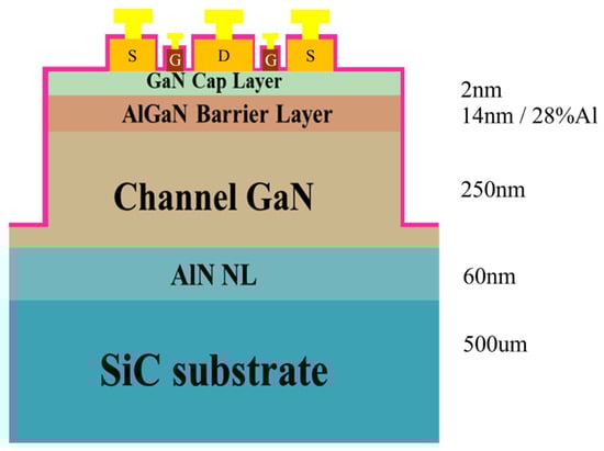
Figure 1.
Cross-sectional schematic illustrating the structure of the fabricated GaN-based T-gate HEMT.
Two distinct T-gate configurations were investigated in this work. For Sample A, the T-gate structure was fabricated using a dual-layer photoresist system with different sensitivities. In contrast, Sample B incorporated a SiNx layer at the base of the T-gate stem. The gate region—defining both the footprint and gate length—was patterned through electron beam lithography (EBL), followed by etching via RIE to complete the structure definition.
Both fabricated devices possessed a gate length (LG) of 100 nm and a total gate width (WG) of 50 μm × 2, with symmetric gate-to-source (LGs) and gate-to-drain (LGD) spacings of 1.6 μm.
3. Results and Discussion
3.1. GaN-HEMTs DC Characteristics
Figure 2 presents the linear-scale transfer characteristics and corresponding transconductance (Gm) for Samples A and B. The threshold voltage (Vth) was extracted at a drain current density of 1 mA/mm, taking specific contact resistance into account. Sample A exhibited a Vth of –3.6 V and a peak Gm of 319 mS/mm, while Sample B showed a Vth of –2.9 V and a peak Gm of 259 mS/mm. Figure 3 shows the output characteristics with the gate voltage (VGS) swept from −5 V to 5 V. Sample A achieves a maximum drain saturation current density (JDS, max) of 1561 mA/mm, which is slightly higher than that of Sample B at 1175 mA/mm. The corresponding ON-resistances (Ron) are 3.5 ohm-mm and 3.3 ohm-mm, respectively.
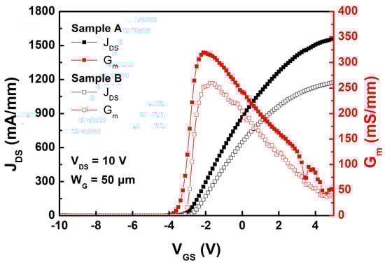
Figure 2.
Comparison of the transfer and transconductance (Gm) characteristics for Samples A and B.
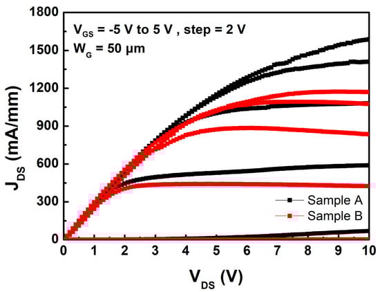
Figure 3.
Output characteristics comparison between Samples A and B.
Figure 4 illustrates the transfer characteristics and gate leakage current plotted on a logarithmic scale. The on/off current ratios are 1.2 × 10⁴ for Sample A and 3 × 10⁶ for Sample B, indicating better off-state suppression in Sample B. The subthreshold swing (SS) was extracted from the log-scale transfer curve by analyzing five data points in the subthreshold region (JDS < 1 mA/mm). The extracted SS values are 438 mV/dec and 167 mV/dec for Samples A and B, respectively, suggesting weaker gate control in Sample A. The gate leakage current at VGS = 5 V was measured to be 3.7 × 10⁻⁴ mA/mm for Sample A and 1 × 10⁻³ mA/mm for Sample B.
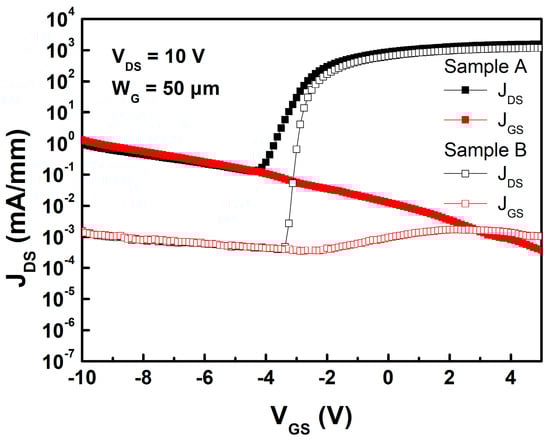
Figure 4.
Comparison of the transfer characteristics and gate leakage current (in logarithmic scale) for Samples A and B.
3.2. GaN-HEMTs Small Signal Performance
Figure 5a,b present the small-signal characteristics of Samples A and B, specifically illustrating fT and fmax. Measurements were performed under a bias condition of (VGS, VDS) = (−2 V, 10 V), where the gate voltage was selected to correspond to the peak transconductance (Gm, max) for both samples. Sample A achieved fT and fmax values of 82.7 GHz and 80.2 GHz, respectively, while Sample B exhibited lower values of 66.2 GHz and 50.1 GHz.
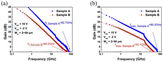
Figure 5.
(a) Current gain and (b) maximum available gain versus frequency for Samples A and B. Sample A shows higher fT and fmax due to lower parasitic effects.
The superior high-frequency performance of Sample A is primarily attributed to its reduced parasitic capacitances. Smaller capacitances result in lower signal propagation delays, thereby directly improving the device’s frequency response. In addition, reduced parasitic capacitance leads to shorter carrier transit times and faster signal transitions, collectively contributing to the higher fT and fmax observed in Sample A.
This improvement is closely related to the gate structure. The floating T-gate used in Sample A provides superior electrostatic control and lower overlap capacitance compared to the conventional T-gate fabricated on a SiNx dielectric layer. This structural advantage effectively reduces parasitic effects, enhances signal integrity, and supports high-speed operation. Therefore, the floating T-gate architecture is particularly well suited for high-frequency and millimeter-wave applications, such as next-generation RF front ends and 5G base stations. Table 1 summarizes key characteristics and measured data of both samples for easy comparison.

Table 1.
Summary of key DC and small-signal characteristics of Samples A and B for performance comparison.
4. Conclusions
We report the successful realization of two variants of 100 nm T-gate AlGaN/GaN HEMTs fabricated on SiC substrates, followed by a thorough investigation of their DC and RF behavior. To improve high-frequency performance, a floating T-gate configuration was implemented by removing the conventional SiNx supporting layer, effectively lowering the parasitic capacitance. Experimental observations show that this structural modification enhances the peak drain current from 1175 mA/mm to 1561 mA/mm and raises the transconductance from 259 mS/mm to 319 mS/mm. In RF characterization, the floating T-gate device exhibits fT of 82.7 GHz and fmax of 80.2 GHz. These results clearly demonstrate that the gate configuration plays a crucial role in determining RF performance, validating the potential of the proposed fabrication process for advanced high-power and high-frequency GaN device applications.
Author Contributions
Conceptualization, Y.-C.L. and M.-C.W.; investigation, H.-C.H. and I.-H.W.; formal analysis, Y.-C.L. and D.-Y.W.; data curation, Y.-C.L., H.-C.H. and I.-H.W.; writing—original draft preparation, Y.-C.L.; writing—review and editing, Y.-C.L. and M.-C.W.; supervision, M.-C.W.; project administration, M.-C.W.; funding acquisition, M.-C.W. All authors have read and agreed to the published version of the manuscript.
Funding
This work was supported by the Ministry of Science and Technology, Taiwan, under Grant No. 112-2622-E-007-020.
Institutional Review Board Statement
Not applicable.
Informed Consent Statement
Not applicable.
Data Availability Statement
No new data were created or analyzed in this study.
Conflicts of Interest
The authors declare no conflict of interest.
References
- Miller, N.C.; Bui, K.; Lee, K.H.; Wu, T.; Hicks, R.; Shigesato, G.; Brown, E.R. A survey of GaN HEMT technologies for millimeter-wave low noise applications. IEEE J. Microw. 2023, 3, 1134–1146. [Google Scholar] [CrossRef]
- Mahin, R.; Mahbub, I. A 3.1 W high gain 51% fractional bandwidth GaN HEMT power amplifier design for far-field wireless power transfer (WPT) applications. In Proceedings of the 2023 IEEE Texas Symposium on Wireless and Microwave Circuits and Systems (WMCS), Waco, TX, USA, 27–28 April 2023; pp. 1–5. [Google Scholar] [CrossRef]
- Dubey, S.K.; Islam, A. Analysis of AlGaN/GaN based HEMT for millimeter-wave applications. In Proceedings of the 2022 IEEE International Conference of Electron Devices Society Kolkata Chapter (EDKCON), Kolkata, India, 26–27 November 2022; pp. 547–552. [Google Scholar] [CrossRef]
- Islam, N.; Mohamed, M.F.P.; Khan, M.F.A.J.; Falina, S.; Kawarada, H.; Syamsul, M. Reliability, Applications and Challenges of GaN HEMT Technology for Modern Power Devices: A Review. Crystals 2022, 12, 1581. [Google Scholar] [CrossRef]
- Nahhas, A.M. Review of AlGaN/GaN HEMTs Based Devices. Am. J. Nanomater. 2019, 7, 10–21. [Google Scholar]
- Tian, Z.; Ji, X.; Yang, D.; Liu, P. Research Progress in Breakdown Enhancement for GaN-Based High-Electron-Mobility Transistors. Electronics 2023, 12, 4435. [Google Scholar] [CrossRef]
- Nakajima, S. GaN HEMTs for 5G Base Station Applications. In Proceedings of the 2018 IEEE International Electron Devices Meeting (IEDM), San Francisco, CA, USA, 1–5 December 2018; pp. 14.2.1–14.2.4. [Google Scholar] [CrossRef]
- Lu, H.; Zhang, M.; Yang, L.; Hou, B.; Perez Martinez, R.; Mi, M.; Du, J.; Deng, L.; Wu, M.; Chowdhury, S.; et al. A review of GaN RF devices and power amplifiers for 5G communication applications. Fundam. Res. 2025, 5, 315–331. [Google Scholar] [CrossRef] [PubMed]
- Chen, K.J.; Häberlen, O.; Lidow, A.; Tsai, C.I.; Ueda, T.; Uemoto, Y.; Wu, Y. GaN-on-Si Power Technology: Devices and Applications. IEEE Trans. Electron Devices 2017, 64, 779–795. [Google Scholar] [CrossRef]
- Akshaykranth, A.; Ajayan, J.; Bhattacharya, S.; Nirmal, D.; Paramasivam, S.; Gatto, G.; Kumar, A. Aggressively Scaled T-Gated GaN-on-Silicon RF Power HEMT Featuring Step Graded SRL-AlGaN Buffer for Next Generation Broadband Power Amplifiers. Results Eng. 2025, 25, 104151. [Google Scholar] [CrossRef]
- Jung, H.-W.; Choi, I.-G.; Kim, D.-H.; Jung, H.-S.; Choi, S.-M.; Chang, S.-J.; Ahn, H.-K.; Lim, J.-W.; Kang, D.-M.; Kim, D.-H.; et al. Improved Frequency Performance in AlGaN/GaN HEMTs on Si Using Hydrogen Silsesquioxane-Assisted Gate. Mater. Sci. Semicond. Process. 2024, 170, 107985. [Google Scholar] [CrossRef]
- Androse, D.R.; Deb, S.; Radhakrishnan, S.K.; Sekar, E. T-Gate ALGaN/GaN HEMT with Effective Recess Engineering for Enhancement Mode Operation. Mater. Today Proc. 2021, 45, 3556–3559. [Google Scholar] [CrossRef]
- Bi, L.; Yao, Y.; Jiang, Q.; Huang, S.; Wang, X.; Jin, H.; Dai, X.; Xu, Z.; Fan, J.; Yin, H.; et al. Instability of Parasitic Capacitance in T-Shape-Gate Enhancement-Mode AlGaN/GaN MIS-HEMTs. J. Semicond. 2022, 43, 032801. [Google Scholar] [CrossRef]
- Luo, H.; Zhong, Z.; Hu, W.; Guo, Y. Analysis and Modeling of the Temperature-Dependent Nonlinearity of Intrinsic Capacitances in AlGaN/GaN HEMTs. IEEE Microw. Wirel. Compon. Lett. 2021, 31, 373–376. [Google Scholar] [CrossRef]
Disclaimer/Publisher’s Note: The statements, opinions and data contained in all publications are solely those of the individual author(s) and contributor(s) and not of MDPI and/or the editor(s). MDPI and/or the editor(s) disclaim responsibility for any injury to people or property resulting from any ideas, methods, instructions or products referred to in the content. |
© 2025 by the authors. Licensee MDPI, Basel, Switzerland. This article is an open access article distributed under the terms and conditions of the Creative Commons Attribution (CC BY) license.