


Abstract
In energy-harvesting storage systems, in order to guarantee the correct operation and integration of its parts into the system, different power converters must be used. Using several stages increases energy processing and therefore decreases the overall efficiency of the system. In this paper, an integrated multi-port converter with galvanic isolation is proposed. It allows the transfer of energy between the solar panel, the battery, and the user using the fewest possible stages, thus maximizing efficiency. Operating in three modes depending on the battery’s state of charge, solar radiation and load conditions, the converter can conduct electric power between its ports. The proposal was validated in a 1 kW prototype performing the different modes of operation. It should be noted that a PV emulator (ETS150X5.6C-PVF) was used in the experimental setup; by means of this device, conditions such as solar irradiance and temperature, which affect the energy generation of PV panels, were controlled. In addition, the transformer employed in the prototype implementation was handmade; therefore, its design could be improved to obtain better performance. The experimental results show efficiencies exceeding 94%, and an analysis of the distribution of losses in the circuit was carried out. Also, a comparison with previous proposals is presented, showing competitive features.
1. Introduction
One of the most pressing problems worldwide today is global warming. It affects all countries on all continents, causing a negative impact on their economies, people’s lives, and their communities. Climate change has spurred various sectors toward the development and promotion of renewable energies at different stages of the electric system as one of the solutions to mitigate greenhouse gas emissions. One of these alternatives is distributed generation (DG) based on renewable energies, whose philosophy is to locate energy sources closer to consumption centers [1]. This alternative provides both technical and environmental benefits. Among its main advantages are the following [2]:
- Reduction in losses in electric transmission and distribution lines.
- Improvement in voltage profiles in distribution circuits.
- Reduction in the need for circuit expansion.
- Control of reactive power injection.
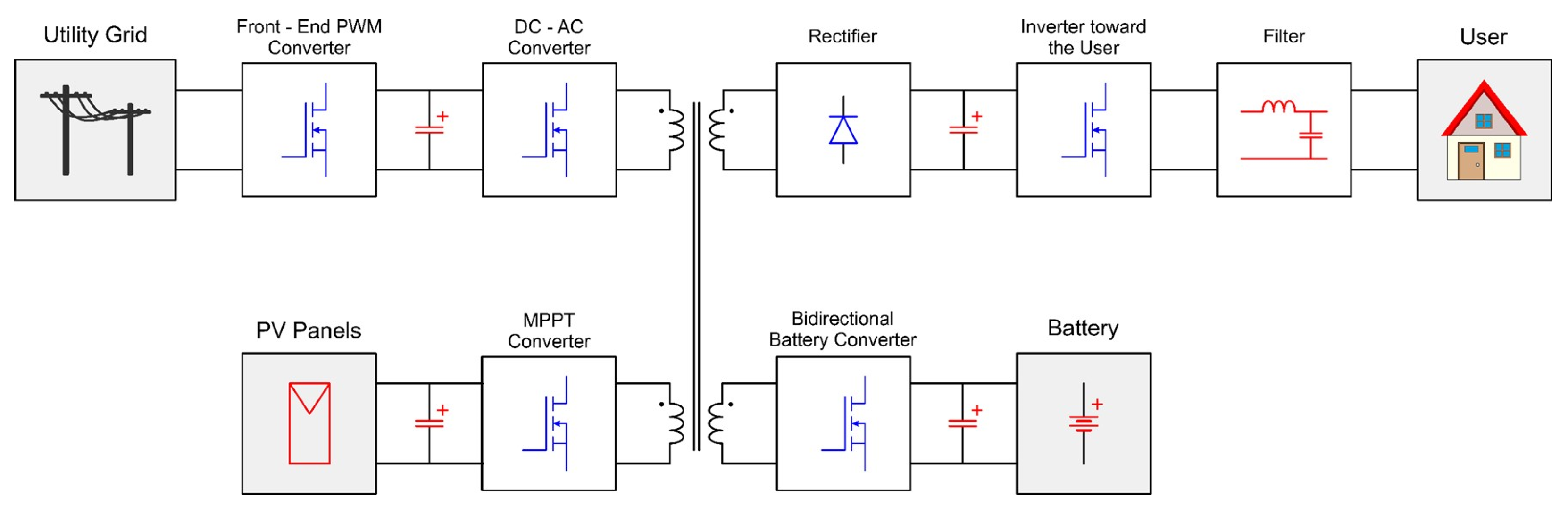
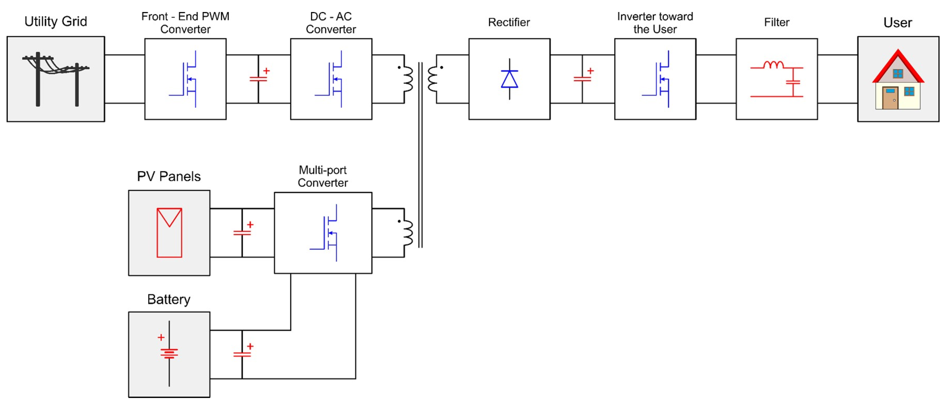
In distributed generation systems, one of the most widely used is grid-connected solar systems. Figure 1 depicts the typical general scheme of these systems [3]. The system includes as energy sources the utility grid, solar energy and a battery-based energy storage system. The integration of different energies sources makes it a complex system. But it has the advantage that the user is always energized, at least while the battery is charged, even during a natural disaster. In this type of system, by safety regulatory requirements, galvanic isolation is mandatory on the electrical grid side.
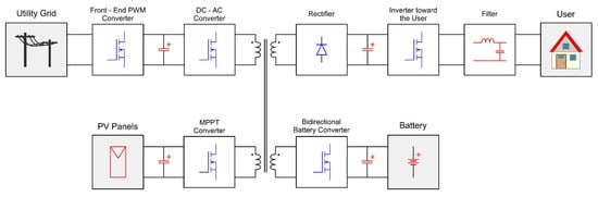
Figure 1.
Isolated grid-connected PV topology with integrated storage.
One of the main drawbacks in this scheme is efficiency due to the multiple stages. For example, in the scheme of Figure 1, when energy needs to be transferred from the PV panel to the battery, it must pass through both the MPPT converter (which connects the PV panel to the transformer) and the bidirectional battery converter (which connects the battery to the transformer). The use of multiple stages enhances the control capability of the topology but considerably diminishes the overall efficiency of the system.
In [4], a converter based on a solid-state transformer is used to achieve isolated interconnection to the utility grid, the PV panels, and the storage system. This topology employs different converters with independent control in each part of the system. This allows an optimization of control goals in each stage but increases the number of stages that must process energy as it moves from one point to another. Therefore, the overall system efficiency is reduced. Additionally, it inevitably raises the cost of the system.
An alternative to this type of system is the use of multi-port converters [5,6,7,8,9]. This family of converters shares common elements in their topology across different configurations. This reduces the implementation volume and the energy processed during the exchange between the different ports of the system (Figure 2).
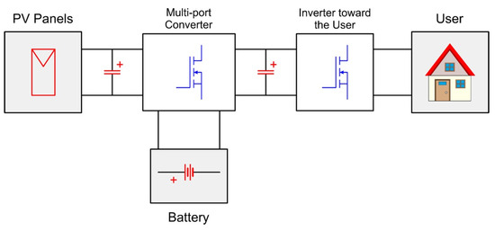
Figure 2.
Typical multi-port converter interface.
To use multi-port converters (MPCs) in photovoltaic applications with storage systems brings a significant advantage over traditional solutions. By employing MPCs, it ensures that through sharing common elements of the same structure, the same functions are performed within a more compact topology.
Among the isolated multi-port converter topologies are the two-winding transformer-coupled MPCs [10,11,12,13,14,15]. This type of topology uses a two-winding transformer with a single regular core, and two or more ports are combined at the primary or secondary terminal of the transformer. Another existing isolated topology is the multiple-winding transformer-coupled MPC [4,16,17,18,19]. These topologies are constructed by combining three or more ports using a single high-frequency transformer with multiple windings, providing isolation for all ports. The main advantage of these topologies is that they provide galvanic isolation between all converter ports and facilitate handling high power and power flow due to the presence of the transformer.
In the literature, there are also MPCs coupled through multiple transformers [20,21], which are achieved by combining two or more transformers to ensure isolation between ports. The main advantage of these topologies is that they allow energy exchange between multiple ports simultaneously, although due to the construction of the transformer, they are generally a more expensive alternative.
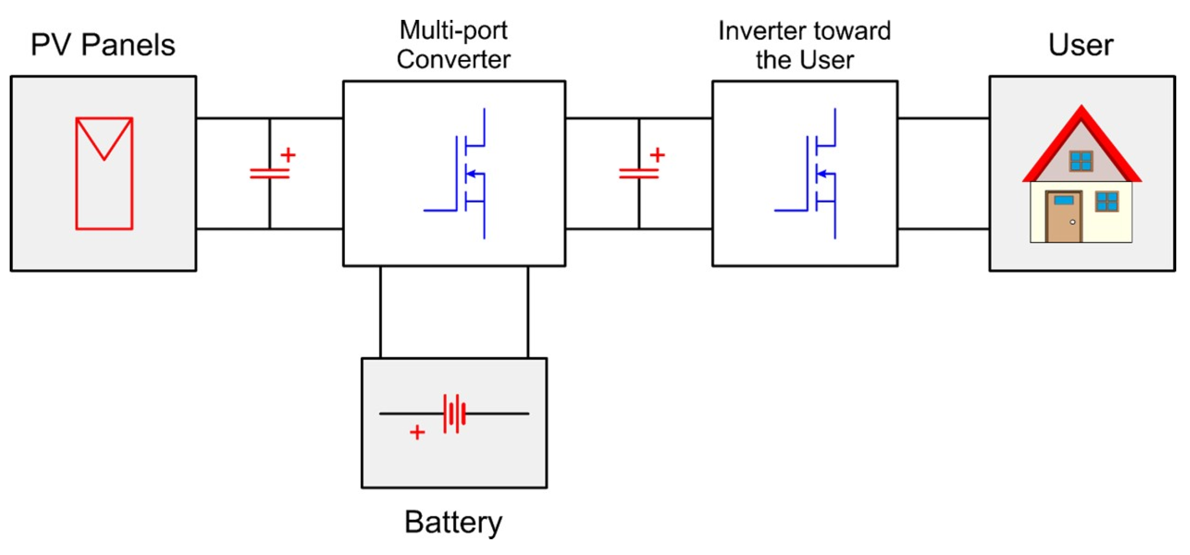
This paper proposes a topology that, reduces the number of energy processing stages while maintaining the basic control capabilities between the energy-generating and storage element, thereby improving efficiency and reducing costs. Building upon the topology shown in Figure 2, the aim is to eliminate one stage in the energy processing when transferring energy between the solar panel and the battery. This results in a topology for the interconnection between the battery, the solar panel, and the user or the grid through a transformer, as depicted in Figure 3. The multi-port converter is responsible for transferring energy from either the solar panels or the battery to the user as well as charging the battery from either the electrical grid or the solar panel.
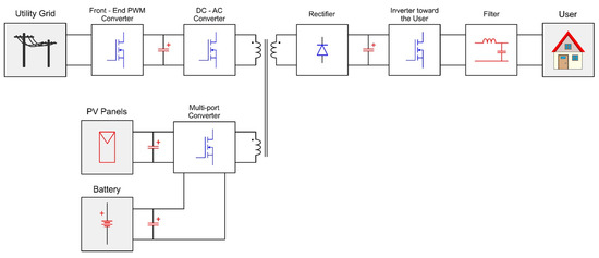
Figure 3.
General scheme with the proposed multi-port converter.
2. Proposed Multi-Port Converter
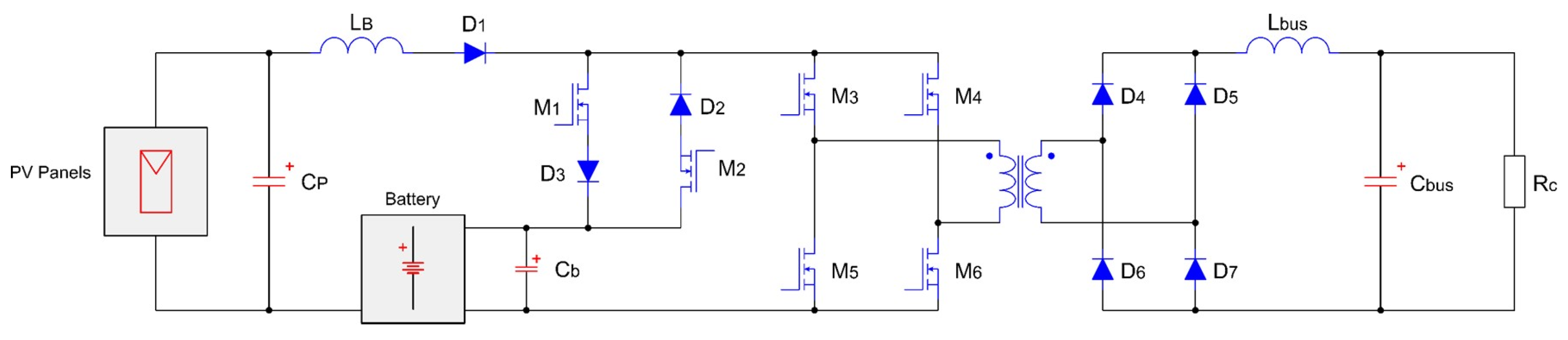
In an effort to reduce the number of electrical power processing stages, it becomes necessary to share components, meaning that certain elements perform multiple functions depending on the operating mode of the converter. This approach may increase the complexity of the converter design and potentially raise implementation costs, since the components cannot be fully optimized for all required functions. Nevertheless, when justified by the application, the initial implementation cost can be amortized through improved overall efficiency. The higher efficiency allows for increasing the output power or to extend the system’s autonomy. One of the fundamental premises for using multi-port converters is their ability to share elements to transfer energy from one port to another. Figure 4 shows the proposed converter, which improves the efficiency by reducing the power stages where the energy is processed, particularly from the PV panels to the battery.
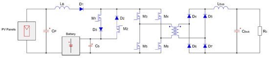
Figure 4.
Proposed multi-port converter.
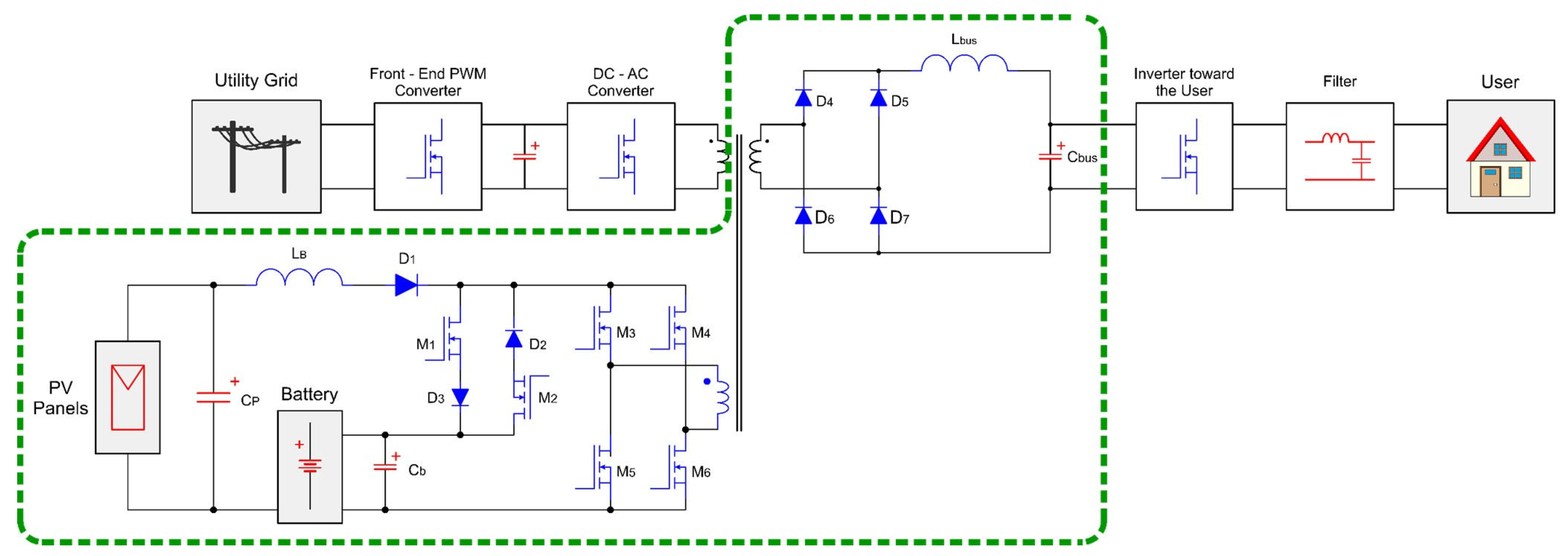
This converter will replace the two stages of energy processing commonly used between the PV panel and the battery, resulting in the general scheme as shown in Figure 5.
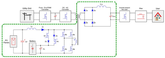
Figure 5.
General scheme including the proposed multi-port converter (inside the green line area).
The proposed converter can operate in three modes:
- PV panels–battery;
- PV panels–DC bus;
- Battery–DC bus.
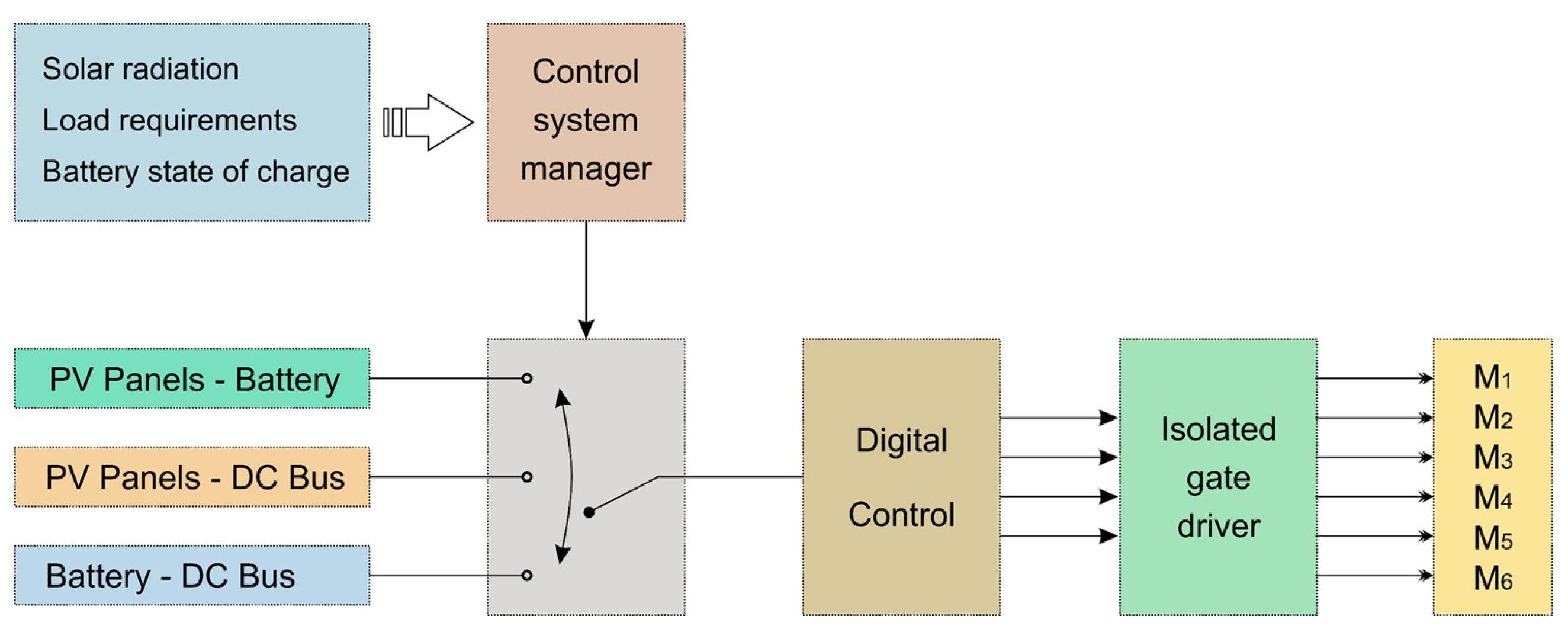
The operating modes of the proposed converter are accomplished by a control circuit manager which guarantees the different modes according to the system conditions (solar radiation, load requirements, and battery state of charge). The structure of the manager system is shown in Figure 6. The control system manager, based on user decisions and measurements, has the authority to make the decision to operate in one or another mode. This circuit controls the semiconductors M1–M6 according to the desired operating mode. The details of the operation will be explained later in this paper.
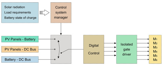
Figure 6.
General control circuit diagram for the proposed converter.
3. Analysis of the Proposed Multi-Port Converter
As mentioned, the proposed converter has three operating modes, which will be analyzed in the following sections.
3.1. PV Panels–Battery Mode
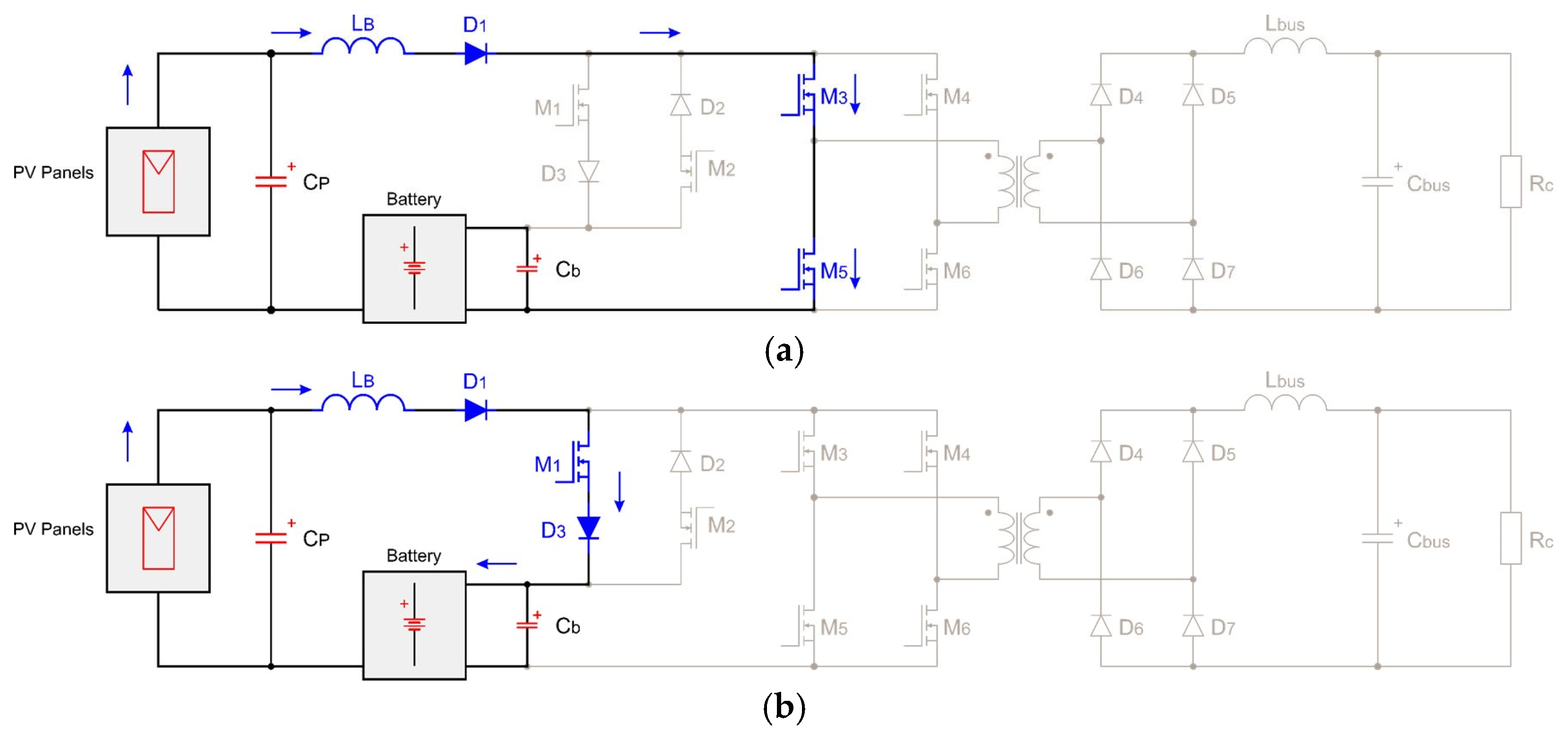
This operation mode takes place when solar radiation exists and the battery is discharged. Assume that the load does not require energy. In the PV panel–battery mode, the equivalent topology is a boost converter; the boost switch is M3 and M5 switched On at the same time (actually, switches M3 to M6 could be the boost switch), the boost inductor is LB, and the freewheeling diode is D3 (M1 is always On in this operation mode). In this operation mode, the Cb capacitor reduces the battery current ripple, increasing its useful life.
Figure 7a shows the energy store stage into the inductor LB. During this stage, M3 and M5 are On. This equivalent circuit is like the On time in the very well-known boost converter. The energy transfer to the battery is shown in Figure 7b. In a common boost converter, the Cb capacitor supplies energy to the load in the inductor LB storing energy stage, but in the PV panel–battery mode, it reduces the current ripple on the battery, increasing its useful life.
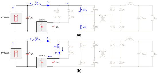
Figure 7.
Proposed multi-port converter in PV panel–battery mode, (a) On time, (b) Off time.
Equation (1) is used to calculate the boost inductor value in this operation mode; however, the final value will be determined by the maximum required by the modes which share this inductance.
where the following apply:
is the voltage in the set of PV panels;
is the boost switch duty cycle in the PV panel–battery mode;
is the desired current ripple on inductance LB;
is the switched frequency in this operation mode.
The duty cycle depends on the ratio between the voltage in the set of PV panels and the battery voltage, that is,
The Cb capacitor is calculated with the following equation.
where the following apply:
is the desired voltage ripple on the Cb capacitor.
This capacitor also functions as a clamp capacitor in the PV panels–DC bus operation mode; so the value to be used will be according to the maximum required. In this operation mode, it is used like a battery current ripple reductor. The control circuit for this operation mode is any battery-charging technique, such as constant current, constant voltage, combination constant current followed by constant voltage, or another advanced battery-charging technique according to the stage of charge of the battery, state of health of the battery, etc.
3.2. PV Panels–DC Bus
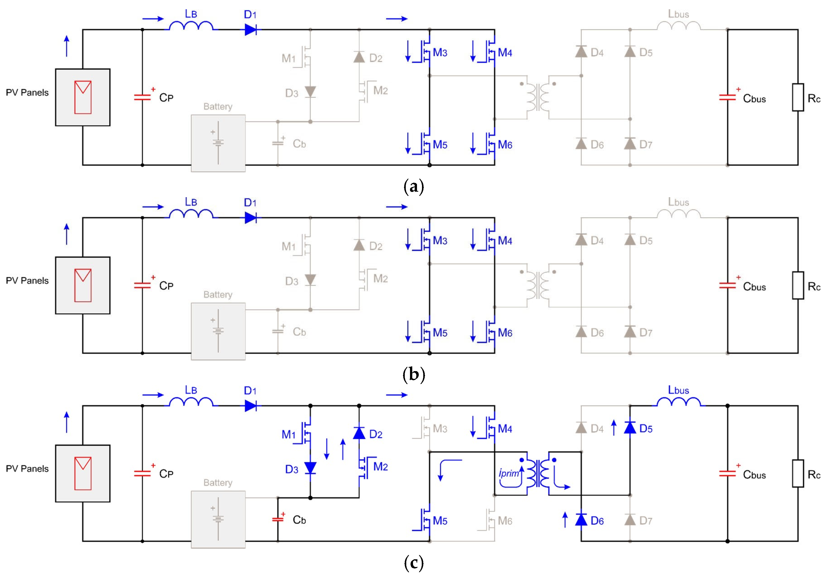
In this operation mode, the user is totally powered by the generated photovoltaic energy. During this operation mode, the equivalent topology is the active–clamp isolated full-bridge boost converter. The active–clamp circuits are M1, M2, D2, D3, and Cb components (see Figure 8). The switches M1 and M2 must be appropriately switched On according to the instantaneous value of the current in the primary side of the transformer and the inductor LB current.
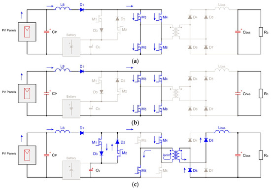
Figure 8.
Proposed multi-port converter in PV panels–DC bus operation mode: (a) boost inductor energy storage, (b) energy transfer toward the secondary with positive current in the transformer primary side, (c) energy transfer toward the secondary with negative current in the transformer primary side.
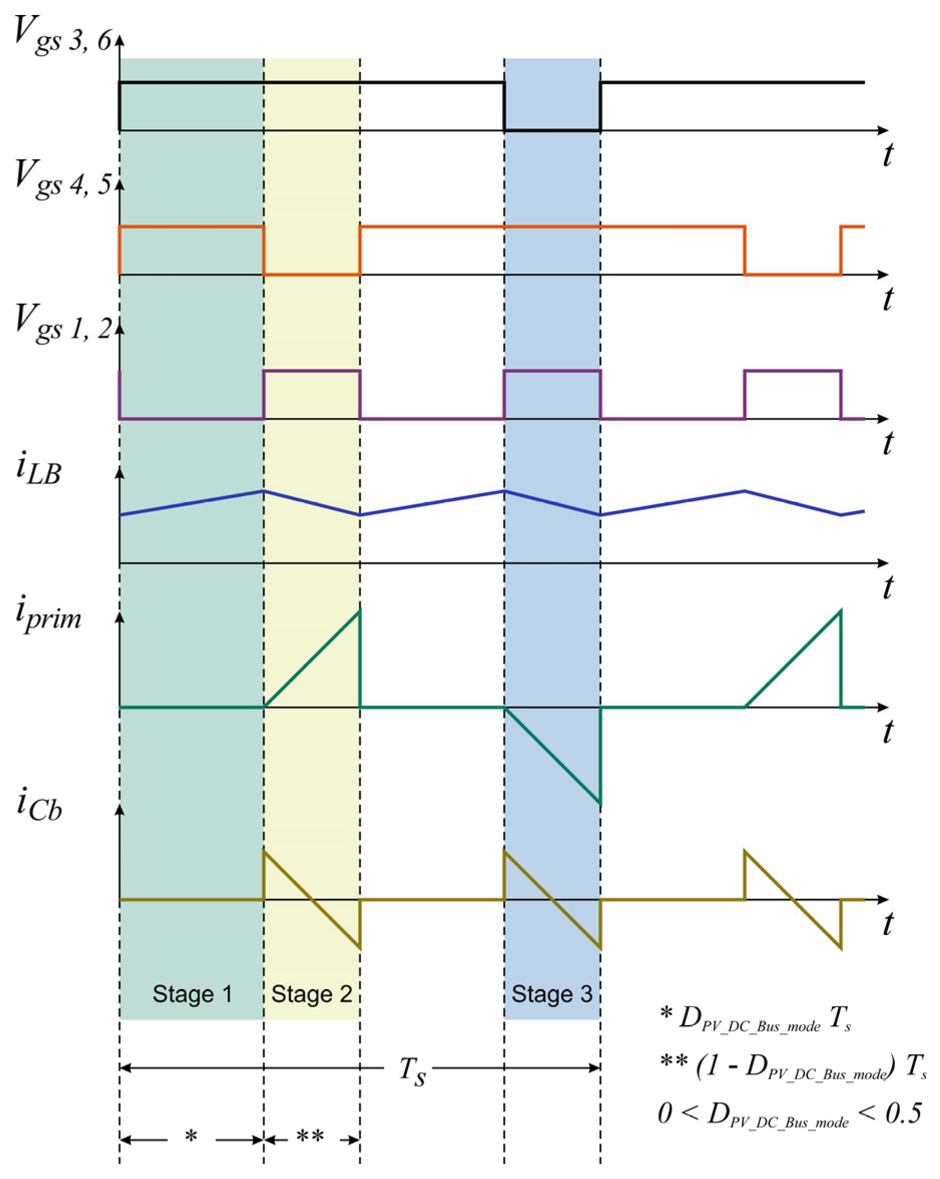
During this operation mode, four stages of operation exist in a switching period (omitting the soft switching details), but two of them are similar. Let us consider three stages: the boost inductor storing energy stage, and two stages in which the energy is transferred to the latter stage, one with positive current in the primary side of the transformer and the other with negative current in the primary side of the transformer.
Figure 8a shows the energy storing time on inductor LB. During this time, the switches M3 to M6 are On simultaneously. Switches M1 and M2 are Off. This stage is like the On time on the boost converter. Figure 8b shows the boost inductor energy transfer toward the secondary (in this case with positive current in the primary side of the transformer, magnetizing the transformer). At the beginning of this stage, the current in the transformer primary side begins from zero, while the boost inductor current is higher than the current in the transformer primary side; then, part of the boost inductor current goes to the clamp capacitor Cb. After that, while the boost inductor current is lower than the current in the transformer primary side, then the clamp capacitor supplies the complementary current. Figure 8c shows the third stage, which is very similar to the second stage, but now the current in the transformer primary side is negative (demagnetizing the transformer).
Figure 9 shows the main waveforms of the equivalent circuit of the converter in the PV panels–DC bus (note that soft-switching operation is omitted by simplification).
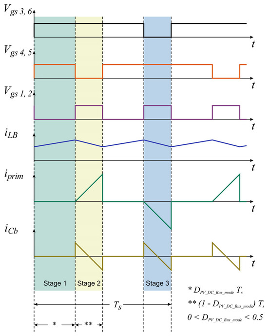
Figure 9.
Key waveforms of the converter in the PV panels–DC bus operation mode.
The boost inductance value in this operation mode is shown below:
where the following apply:
is the duty cycle in the PV panels–DC bus mode;
is the current ripple on boost inductance.
is the switched frequency in this operation mode.
The boost inductance is shared in the PV panels–battery mode and the PV panels–DC bus mode. So, the selected value will be the higher value obtained by Equation (1) or Equation (4). The DC voltage gain ratio of the converter is derived from the operation of the converter in this operation mode, which is obtained from the following equation:
where the following apply:
n is the turns ratio of the transformer;
Lk is the leakage inductance in the primary of the transformer;
Lbus_prim is the Lbus reflected to the primary of the transformer.
The turns ratio of the transformer must be as large as possible to reduce the voltage stress on the primary switches and the current stress on the secondary diodes. This is fulfilled under no-load conditions:
Under this condition, the DC voltage gain is determined simply by the turn ratio of the transformer and the duty cycle. Lbus–Cbus are the output filter components; their values are calculated in the Battery–DC Bus operation mode.
3.3. Battery–DC Bus
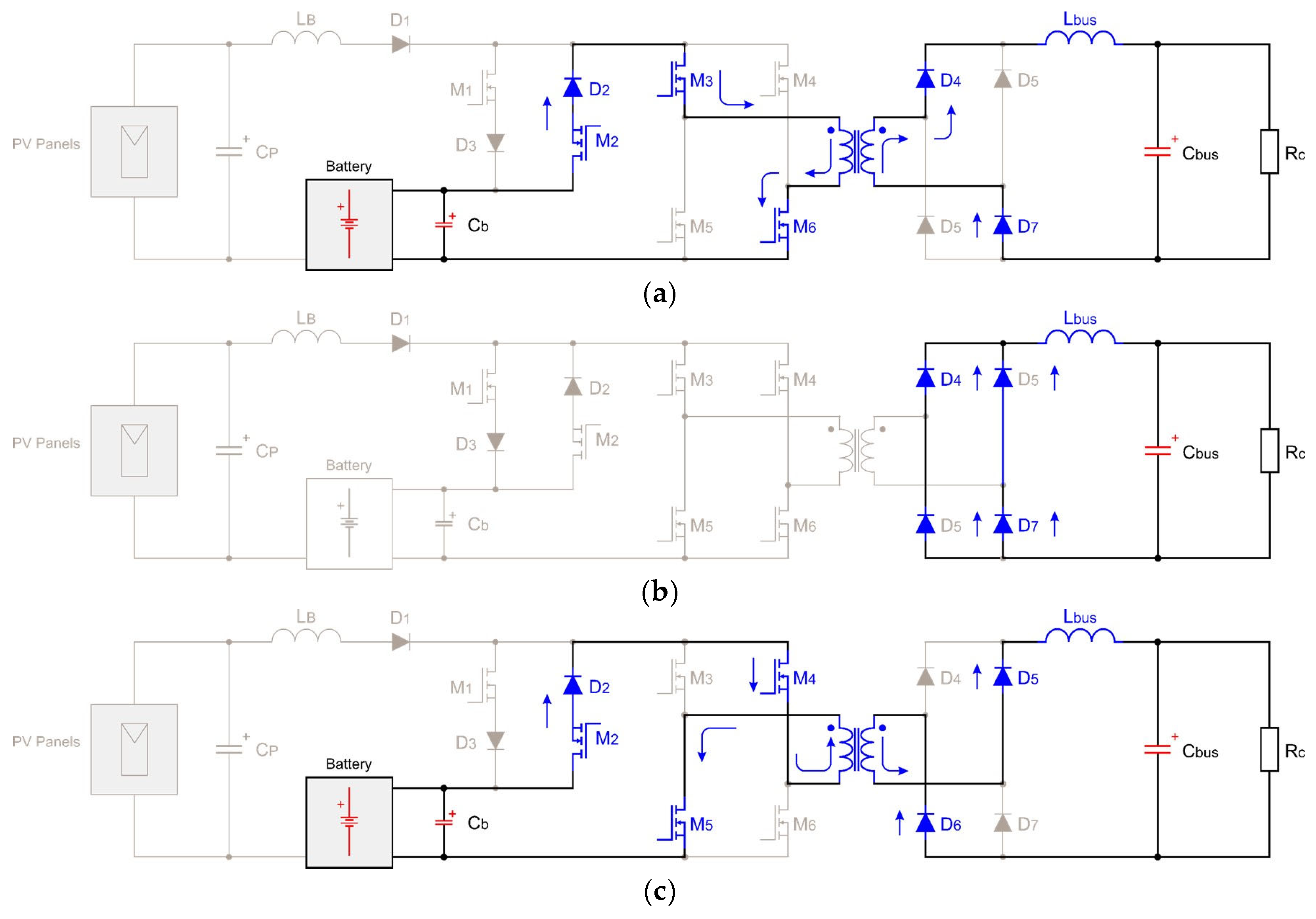
In this operation mode, the load is fed by the stored energy in the battery. The equivalent circuit is the full-bridge converter. In this operation mode, the M1 switch is always Off and M2 is always On. There are four equivalent circuits in a switching period, but two are similar, so let us consider three equivalent circuits.
Figure 10a shows the inductor Lbus energy storing with positive current in the transformer primary side (magnetization of the transformer). Figure 10b shows the energy transfer to the load, and Figure 10c shows the inductor Lbus energy storage with negative current in the transformer primary side (demagnetization of the transformer).
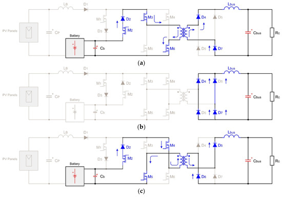
Figure 10.
Proposed multi-port converter in battery–bus mode, (a) energy storage on Lbus with positive current in the transformer, (b) energy transfer to the load, (c) energy storage on Lbus with negative current in the transformer.
In this operation mode the Lbus inductance value is shown below:
where the following apply:
is the duty cycle in the battery–DC bus mode;
is the current ripple on Lb inductance;
is the switching frequency in the battery–DC bus mode.
The duty cycle is calculated from the equation of the DC gain (full-bridge converter), that is,
The output capacitor Cbus is calculated using Equation (9).
where the following applies:
is output ripple in Vbus.
4. Experimental Results
To verify the feasibility of the multi-port converter, an experimental prototype was implemented. The PV panel and battery specifications are shown in Table 1. In the experimental prototype, two PV panels connected in series and ten batteries connected in series were used.

Table 1.
PV panel and battery specifications.
Table 2 shows the parameters used in the experimental prototype.
Table 2.
Parameters for the experimental prototype.
The section mainly presents the results regarding the system’s efficiency, which is the parameter we are looking to improve. In the experimental tests, the PV panels were substituted by a programmable power supply PV simulator. This simulator can emulate PV panels under distinct solar conditions. During the test, the conditions were controlled to a certain state; therefore, constant output power was obtained. While the PV panels were the energy supply for the battery, the power was limited to 500 W so as not to exceed the recommended battery charge current (0.2 C). In the PV panels–DC bus mode, the power was limited to 600 watts, which is close to the limit of the maximum power of the real panel set. In the battery–DC bus mode, the test was carried out from 500 W to 1 kW.
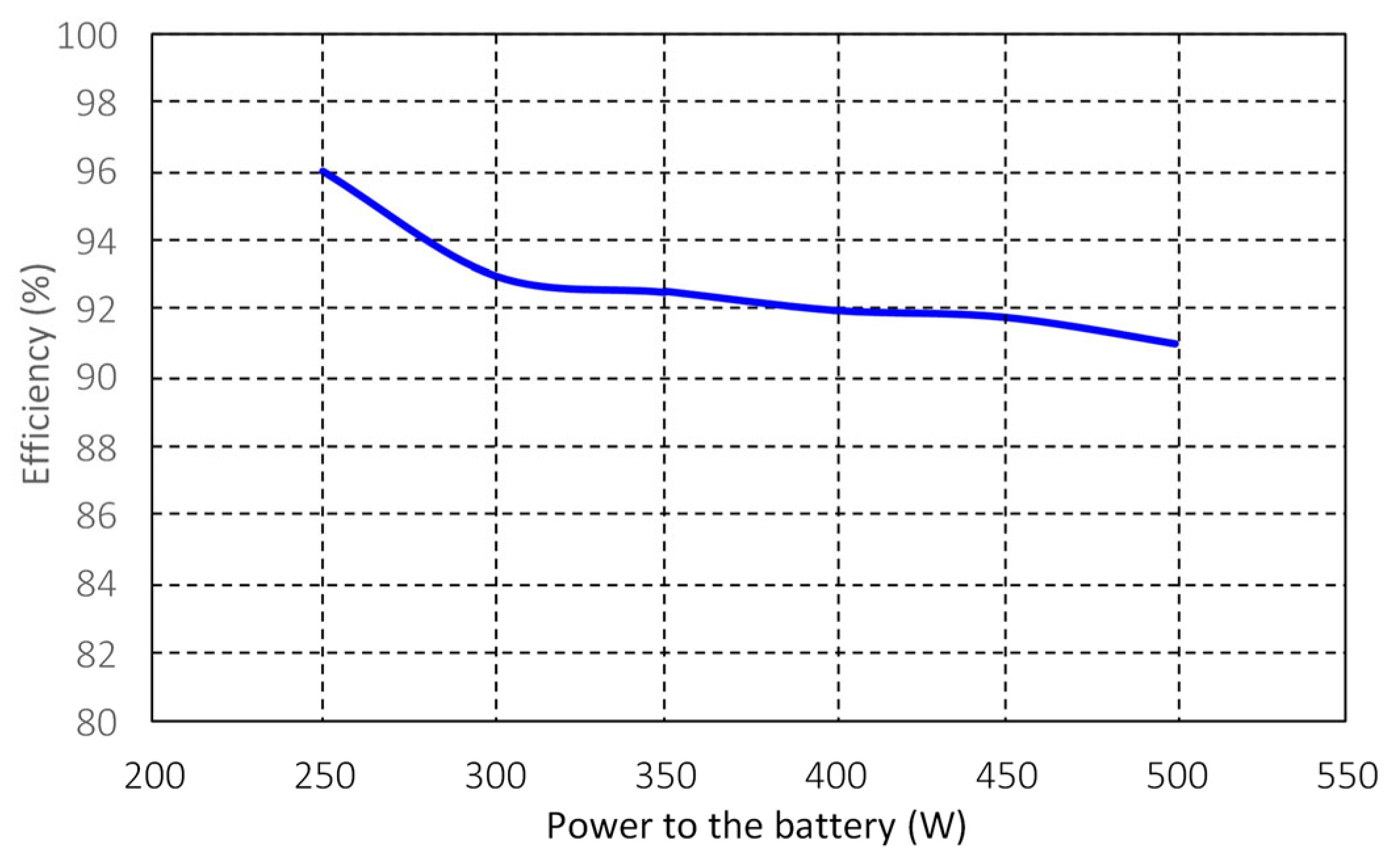
Figure 11 shows the efficiency in the PV panel–battery mode. The highest efficiency was around 96%. The lower efficiency was around 91% (at charge current of 0.2 C approximately). In this operating mode, the equivalent circuit is the boost converter, while the battery is acting as the output load. The voltage difference between the photovoltaics panels and the batteries is small, which is why the efficiency is very high.
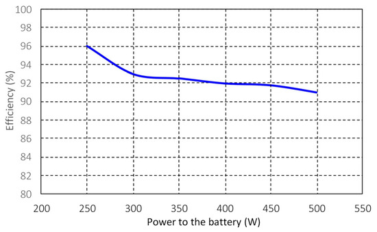
Figure 11.
Efficiency in PV panel–battery mode.
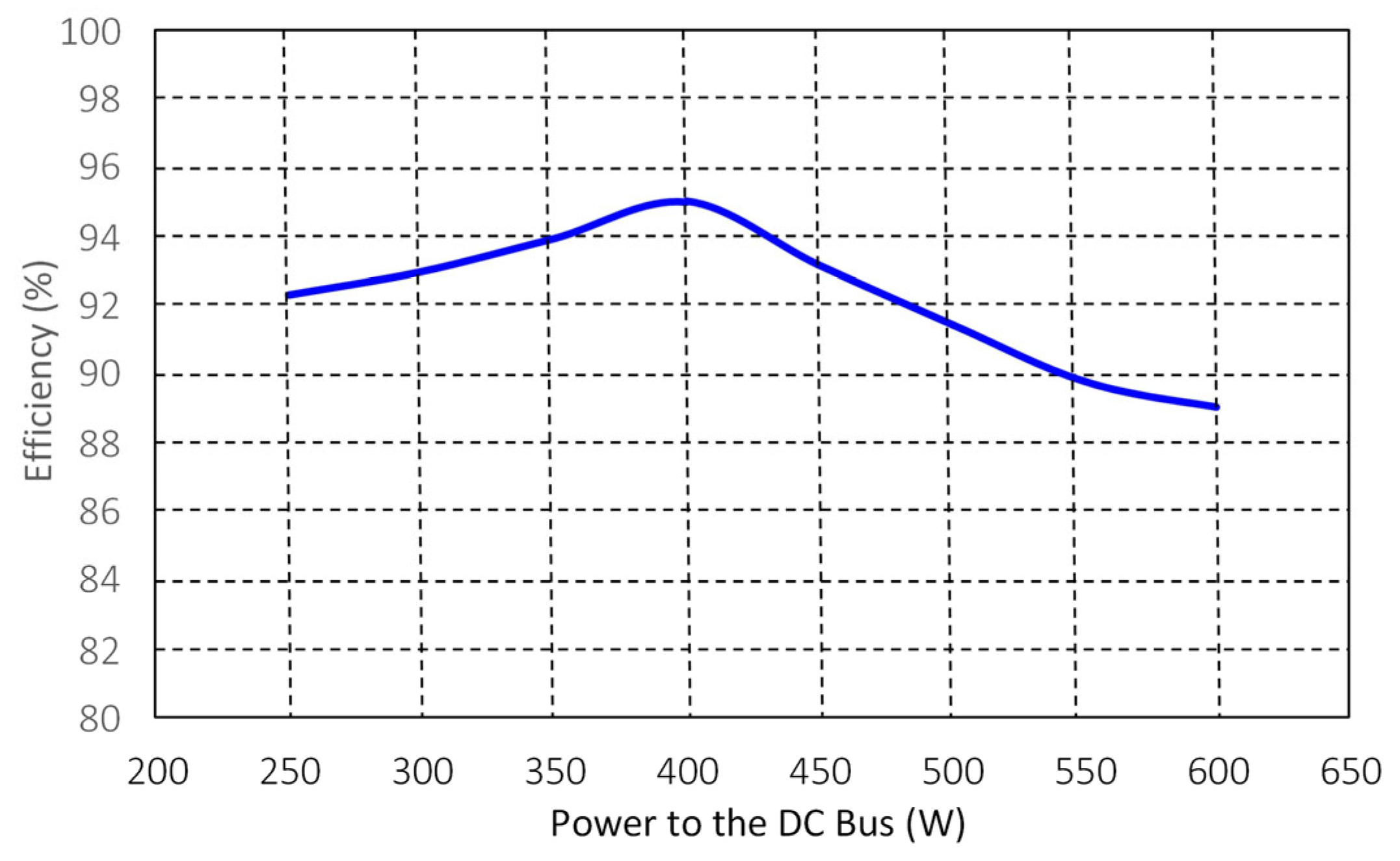
Figure 12 shows the efficiency in the PV panels–DC bus mode. The highest efficiency obtained was around 95%. In the PV panels–DC bus operating mode, the equivalent circuit corresponds to the active-clamp isolated full-bridge boost converter, operating under zero-voltage switching in all power switches. The zero-voltage switching operating condition allows high efficiency.
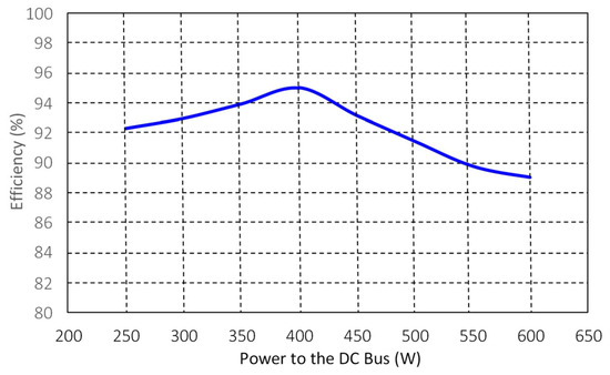
Figure 12.
Efficiency in PV panel–DC bus mode.
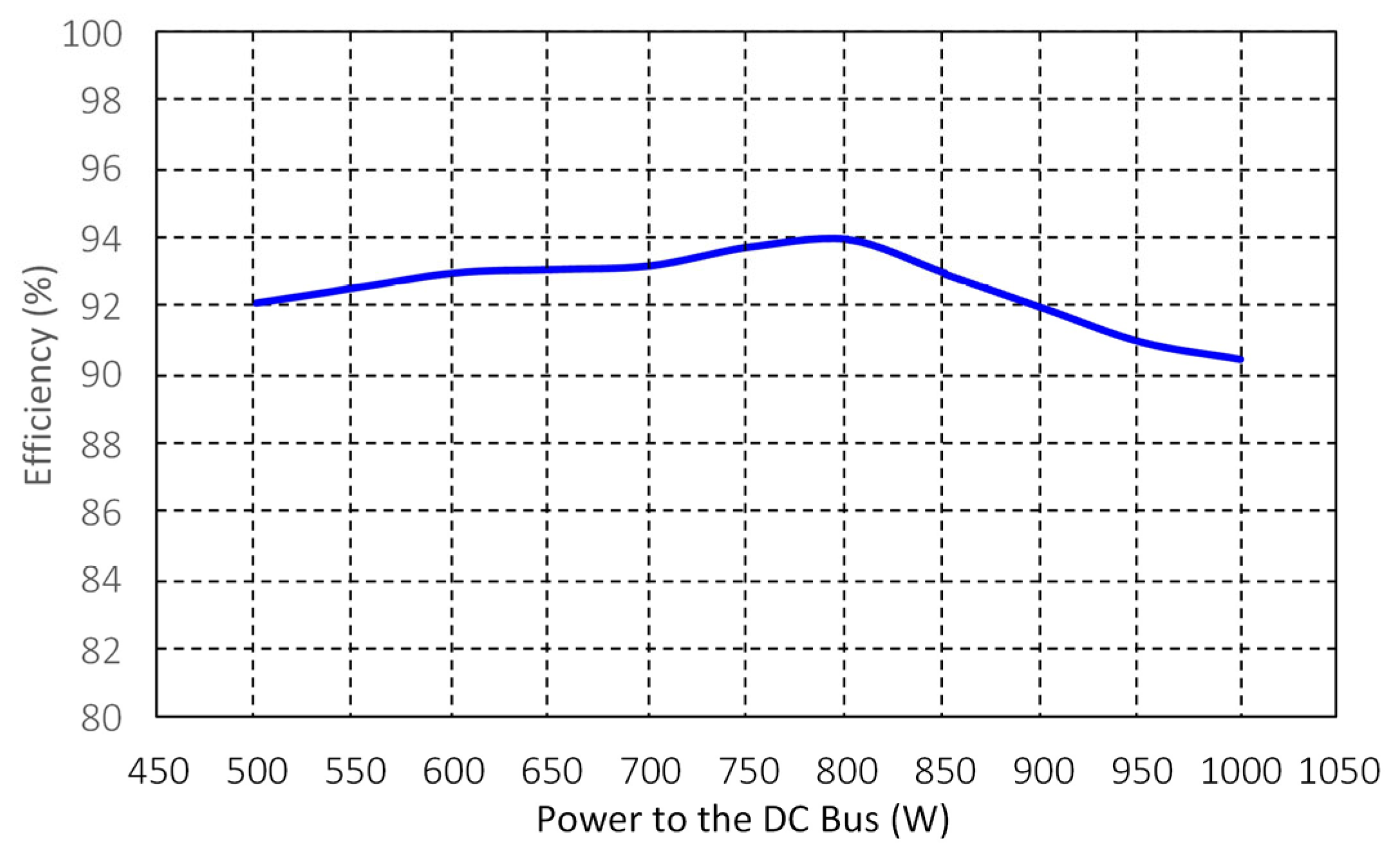
Figure 13 shows the efficiency obtained in the experimental test in the battery–DC bus operation mode. In this case, the equivalent circuit is a boost converter; however, the output is now the DC bus. Since the voltage difference between the input and output is large, the efficiency tends to be lower than that obtained in the PV panel–battery operating mode. In addition, the output power is higher than in the PV panel–battery mode, resulting in higher circulating currents within the converter.
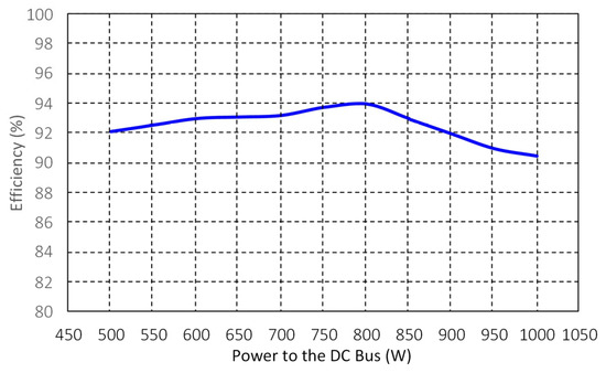
Figure 13.
Efficiency in battery–DC bus mode.
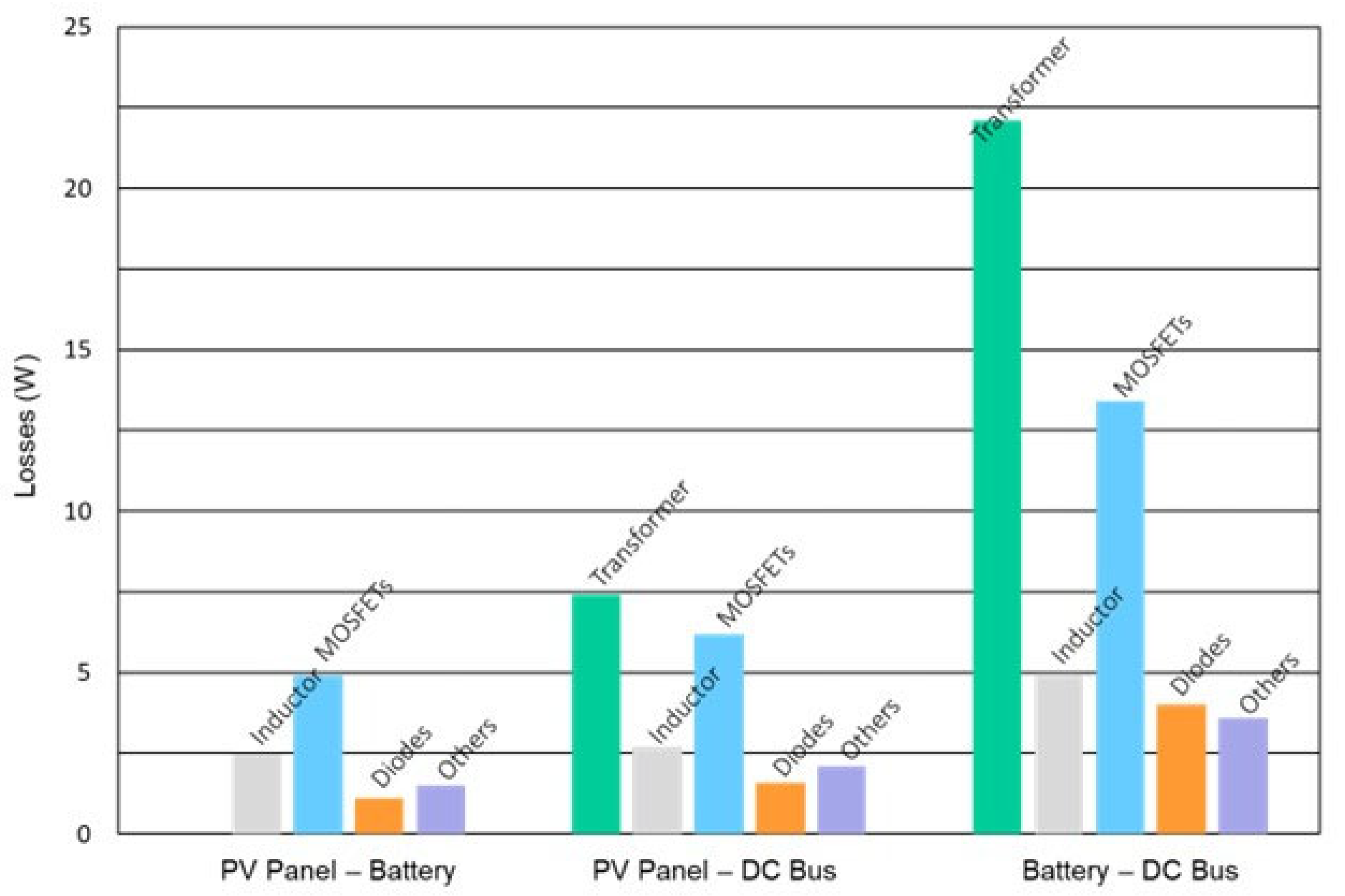
Figure 14 shows the component losses distribution of the proposed converter in the different operations mode at maximum efficiency. The losses of the transformer and inductor were evaluated by measuring the input and output power with the power difference representing the losses. For the semiconductor devices, the oscilloscope’s measurement capabilities were used to determine the input and output power from which the losses were calculated. The highest losses occur in the transformer and the MOSFETs.
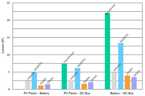
Figure 14.
Losses distribution across the components in the proposed converter in different operation modes.
As previously mentioned, the transformer was hand-made using materials available in the laboratory. Consequently, improving the transformer design and implementation would increase the overall efficiency. In high-frequency transformers, most losses are primarily due to AC resistance rather than DC resistance. Planar transformer technology significantly reduces AC resistance; therefore, it enhances transformer efficiency.
On the other hand, the use of state-of-the-art MOSFET technology is expected to further improve the system’s efficiency.
5. Discussion
In some cases, integrated multi-port converters involve additional complexity and, in some instances, a greater number of components. This is justified when the number of power-processing stages is reduced and the overall efficiency is improved. Table 3 presents a brief comparison of the component count with other proposals focused on multiport converters for PV systems with battery-based energy storage. In general, the component count of the proposed converter is quite similar to that of other proposals. The main difference of the proposed converter is related to the energy-processing stage at which power is transferred.
Table 3.
Component count comparison of multi-port converters with battery-based energy storage.
The use of multi-port converters has significantly contributed to improving the efficiency of photovoltaic systems. Their capability to operate under different modes enables more effective energy management by adapting to variations in solar generation and load demand.
This paper introduces a multi-port converter that interconnects the PV panel, the battery, and the load in both on-grid and off-grid configurations. The main objective of this work is to present an alternative approach for improving system efficiency by reducing the number of energy processing stages, particularly in the battery–DC bus operating mode. Each operating mode is described in detail, including the analytical expressions required for the design of the power stages. In addition, an experimental prototype was implemented to validate the proposed converter and demonstrate its feasibility.
The experimental results show an average efficiency exceeding 94%, which is comparable to values previously reported in the literature. Table 4 presents a comparison with prior works; however, not all publications operating under similar conditions report efficiency data. A loss analysis of the different circuit components reveals that the transformer accounts for the dominant portion of the total losses. In this implementation, the transformer was manually fabricated, leading to higher losses than initially expected. It is anticipated that improvements in transformer manufacturing techniques, together with the adoption of next-generation semiconductor devices, would significantly enhance the overall system efficiency.
Table 4.
Efficiency comparison with previous proposal.
6. Conclusions
In summary, multi-port converters offer a promising solution for addressing the challenges associated with energy management in photovoltaic systems. Their improved efficiency and operational versatility make them a viable and attractive option for constantly evolving photovoltaic applications. With further research and development, their full potential can be harnessed, contributing to the sustainable advancement of solar energy.
In this paper, an integrated multi-port converter is presented. The proposed converter interconnects the photovoltaic panels, the battery-based energy storage system, and the DC bus. Locating the battery within the converter reduces the number of energy processing stages, thereby improving efficiency during battery charging. The proposed topology exploits the active-clamp section and the power switches of an active-clamp full-bridge boost converter to implement both the battery charging and discharging stages. This level of integration contributes to an improvement in the overall system efficiency.
However, reducing the number of power-processing stages requires component sharing, whereby certain elements must perform multiple functions depending on the converter operating mode. This approach increases the design complexity and may raise implementation costs, as shared components cannot be optimally designed for all operating conditions. In the practical implementation, the transformer was required to fulfill multiple functions, making its optimization particularly challenging. This limitation may affect the practical applicability of the proposed converter.
Author Contributions
Conceptualization, D.M. and C.A.; validation, D.M. and J.D.M.; writing—review and editing, D.M., J.E.A., R.A.V. and C.A.; investigation: C.A. and G.L.O. All authors have read and agreed to the published version of the manuscript.
Funding
This research received no external funding.
Institutional Review Board Statement
Not applicable.
Informed Consent Statement
Not applicable.
Data Availability Statement
The original contributions presented in this study are included in the article. Further inquiries can be directed to the corresponding author.
Conflicts of Interest
The authors declare no conflict of interest.
References
- Walling, R.; Saint, R.; Dugan, R.; Burke, J.; Kojovic, L. Summary of Distributed Resources Impact on Power Delivery Systems. IEEE Trans. Power Deliv. 2008, 23, 1636–1644. [Google Scholar] [CrossRef]
- Zobaa, A.; Cecati, C. A Comprehensive Review on Distributed Power Generation. In Proceedings of the International Symposium on Power Electronics, Electrical Drives, Automation and Motion, SPEEDAM 2006, Taormina, Italia, 23–26 May 2006; pp. 514–518. [Google Scholar]
- Narayanaswamy, J.; Mandava, S. Non-Isolated Multiport Converter for Renewable Energy Sources: A Comprehensive Review. Energies 2023, 16, 1834. [Google Scholar] [CrossRef]
- Falcones, S.; Ayyanar, R.; Mao, X. A DC–DC Multiport Converter Based Solid State Transformer Integrating Distributed Generation and Storage. IEEE Trans. Power Electron. 2013, 28, 2192–2202. [Google Scholar] [CrossRef]
- Almutairi, A.; Sayed, K.; Albagami, N.; Abo-Khalil, A.G.; Saleeb, H. Multi-Port PWM DC-DC Power Converter for Renewable Energy Applications. Energies 2021, 14, 3490. [Google Scholar] [CrossRef]
- Chandrasekar, A.; Subramanian, V.; Rajamanickam, N.; Shorfuzzaman, M.; Emara, A. Design and Control of Four-Port Non-Isolated SEPIC Converter for Hybrid Renewable Energy Systems. Sustainability 2024, 16, 8423. [Google Scholar] [CrossRef]
- Koroglu, T.; Ekici, E.; Savrun, M.M. Five-Port Isolated Bidirectional DC-DC Converter for Interfacing a Hybrid Photovoltaic–Fuel Cell–Battery System with Bipolar DC Microgrids. Electronics 2024, 13, 1036. [Google Scholar] [CrossRef]
- Yildirim, B.; Elgendy, M.A.; Smith, A.; Kulan, M.C.; Akbal, B. Modular-Multi-Port-Converter-Based Battery Energy Storage System with Integrated Battery Management Functions. Energies 2025, 18, 3142. [Google Scholar] [CrossRef]
- Shi, C.; Wang, S. A Study on the Device Topology and Control Strategy of a Hybrid Three-Port Photovoltaic Energy Storage Grid-Connected Converter. Electronics 2025, 14, 1966. [Google Scholar] [CrossRef]
- Wu, H.; Chen, R.; Zhang, J.; Xing, Y.; Hu, H.; Ge, H. A Family of Three-Port Half-Bridge Converters for a Stand-Alone Renewable Power System. IEEE Trans. Power Electron. 2011, 26, 2697–2706. [Google Scholar] [CrossRef]
- Qian, Z.; Abdel-Rahman, O.; Hu, H.; Batarseh, H. An Integrated Three-Port Inverter for Stand-Alone PV Applications. In Proceedings of the 2010 IEEE Energy Conversion Congress and Exposition, Atlanta, GA, USA, 12–16 September 2010; pp. 1471–1478. [Google Scholar]
- Al-Atrash, H.; Tian, F.; Batarseh, I. Tri-Modal Half-Bridge Converter Topology for Three-Port Interface. IEEE Trans. Power Electron. 2007, 22, 341–345. [Google Scholar] [CrossRef]
- Shen, C.-L.; Chen, L.-Z.; Chen, G.-Y.; Yang, C.-M. Multi-Port Multi-Directional Converter with Multi-Mode Operation and Leakage Energy Recycling for Green Energy Processing. Energies 2022, 15, 5629. [Google Scholar] [CrossRef]
- Soldado-Guamán, J.; Herrera-Perez, V.; Pacheco-Cunduri, M.; Paredes-Camacho, A.; Delgado-Prieto, M.; Hernandez-Ambato, J. Multiple Input-Single Output DC-DC Converters Assessment for Low Power Renewable Sources Integration. Energies 2023, 16, 1652. [Google Scholar] [CrossRef]
- Wu, H.; Sun, K.; Chen, R.; Hu, H.; Xing, Y. Full-Bridge Three-Port Converters with Wide Input Voltage Range for Renewable Power Systems. IEEE Trans. Power Electron. 2012, 27, 3965–3974. [Google Scholar] [CrossRef]
- Chen, Y.-M.; Liu, Y.-C.; Wu, F.-Y. Multi-input DC/DC Converter Based on the Multiwinding Transformer for Renewable Energy Applications. IEEE Trans. Ind. Appl. 2002, 38, 1096–1104. [Google Scholar] [CrossRef]
- Granata, S.; Di Benedetto, M.; Terlizzi, C.; Leuzzi, R.; Bifaretti, S.; Zanchetta, P. Power Electronics Converters for the Internet of Energy: A Review. Energies 2022, 15, 2604. [Google Scholar] [CrossRef]
- Itoh, K.; Ishigaki, M.; Yanagizawa, N.; Tomura, S.; Umeno, T. Analysis and design of a multiport converter using a magnetic coupling inductor technique. IEEE Trans. Ind. Appl. 2015, 51, 1713–1721. [Google Scholar] [CrossRef]
- Pham, V.-L.; Wada, K. Applications of Triple Active Bridge Converter for Future Grid and Integrated Energy Systems. Energies 2020, 13, 1577. [Google Scholar] [CrossRef]
- Asa, E.; Colak, K.; Bojarski, M.; Czarkowski, D. Asymmetrical duty-cycle and phase-shift control of a novel multiport CLL resonant converter. IEEE J. Emerg. Sel. Top. Power Electron. 2015, 3, 1122–1131. [Google Scholar] [CrossRef]
- Jakka, V.N.S.R.; Shukla, A.; Demetriades, G.D. Dual-Transformer-Based Asymmetrical Triple-Port Active Bridge (DT-ATAB) Isolated DC-DC Converter. IEEE Trans. Ind. Electron. 2017, 64, 4549–4560. [Google Scholar] [CrossRef]
- Marei, M.I.; Alajmi, B.N.; Abdelsalam, I.; Ahmed, N.A. An Integrated Topology of Three-Port DC-DC Converter for PV-Battery Power Systems. IEEE Open J. Ind. Electron. Soc. 2022, 3, 409–419. [Google Scholar] [CrossRef]
- Shi, S.; Xu, S.; Jiang, W.; Hashimoto, S. Design and Analysis of a Step-Up Multi-Port Converter Applicable for Energy Conversion in Photovoltaic Battery Systems. Energies 2024, 17, 223. [Google Scholar] [CrossRef]
- Wang, P.; Lu, X.; Wang, W.; Xu, D. Hardware Decoupling and Autonomous Control of Series-Resonance-Based Three-Port Converters in DC Microgrids. IEEE Trans. Ind. Appl. 2019, 55, 3901–3914. [Google Scholar] [CrossRef]
- Santoro, D.; Kortabarria, I.; Toscani, A.; Concari, C.; Cova, P.; Delmonte, N. PV Modules Interfacing Isolated Triple Active Bridge for Nanogrid Applications. Energies 2021, 14, 2854. [Google Scholar] [CrossRef]
- Zhu, H.; Zhang, D.; Athab, H.S.; Wu, B.; Gu, Y. PV Isolated Three-Port Converter and Energy-Balancing Control Method for PV-Battery Power Supply Applications. IEEE Trans. Ind. Electron. 2015, 62, 3595–3606. [Google Scholar] [CrossRef]
- Mira, M.C.; Zhang, Z.; Knott, A.; Andersen, M.A.E. Analysis, Design, Modeling, and Control of an Interleaved-Boost Full-Bridge Three-Port Converter for Hybrid Renewable Energy Systems. IEEE Trans. Ind. Electron. 2015, 62, 3595–3606. [Google Scholar] [CrossRef]
Disclaimer/Publisher’s Note: The statements, opinions and data contained in all publications are solely those of the individual author(s) and contributor(s) and not of MDPI and/or the editor(s). MDPI and/or the editor(s) disclaim responsibility for any injury to people or property resulting from any ideas, methods, instructions or products referred to in the content. |
© 2026 by the authors. Licensee MDPI, Basel, Switzerland. This article is an open access article distributed under the terms and conditions of the Creative Commons Attribution (CC BY) license.