Abstract
Recent advancements in nanotechnology have intensified research efforts to address security concerns like hardware trojans and intellectual property (IP) piracy, particularly by exploring novel alternatives to traditional MOSFET devices. Spin-based devices, known for their low power consumption, non-volatility, and seamless integration with silicon substrates, have emerged as promising candidates. This research proposes a novel approach to enhance the security of integrated circuits using spin-based devices known as magnetic tunnel junctions (MTJs). A Non-volatile Polymorphic Logic (NPL) is optimized and designed to perform multiple operations, effectively concealing its true functionality. The analytical studies conducted on the Cadence Virtuoso platform using TSMC 65 nm MOS technology demonstrate the feasibility and efficacy of the proposed approach. The proposed NPL circuit enables polymorphism by allowing the circuit to perform all one- and two-input Boolean logic operations, including NOT, AND/NAND, OR/NOR, and XOR/XNOR, through adjustments of applied keys. This dynamic functionality makes it challenging for attackers to determine the circuit’s true operation. The proposed design exhibits similar timing characteristics for different logic operations, which further complicates the tampering attempts. Additionally, the circuit’s layout is designed to be symmetric, ensuring the execution of all possible operations by the same physical layout. This provides post-manufacturing security from reverse engineering and finds its applications in securing custom IC designs against the evolving landscape of hardware-based threats.
1. Introduction
The landscape of custom integrated circuit (IC) design has undergone a profound transformation in recent years, driven by the rapid and expansive growth of embedded systems across various industries. This globalization of IC design has introduced significant complexities, particularly as technology nodes have scaled down to the nanometer range, leading to an exponential increase in fabrication costs. As a result, only a handful of semiconductor manufacturers now possess the resources and capabilities to control the entire supply chain, from the design and production of each component to the final packaging of the ICs. These leading manufacturers dominate the market, while many others have shifted away from in-house fabrication, choosing instead to outsource their manufacturing needs. Outsourcing fabrication to third-party facilities has become an attractive option for many IC designers due to its cost-effectiveness and the potential for faster production cycles [1]. However, this reliance on external and often untrustworthy fabrication facilities introduces substantial security vulnerabilities into the IC supply chain. Untrusted fabrication environments are prone to various security threats, which pose significant risks to the integrity and reliability of the final product. Among the most pressing security concerns are the potential for reverse engineering (RE), where attackers attempt to deduce the design and functionality of a circuit to replicate or alter it. Additionally, counterfeiting and cloning of ICs have become pervasive issues, leading to unauthorized duplication and distribution of critical components. Overproduction, where more units are produced than originally intended, can flood the market with unauthorized products, further complicating supply chain management. Furthermore, the threat of intellectual property (IP) theft looms large, with untrusted facilities having the opportunity to steal or copy proprietary designs, leading to significant financial losses and compromised technological leadership. Perhaps most concerning is the insertion of hardware Trojans—malicious modifications to the circuitry that can remain undetected until activated under specific conditions. These Trojans can compromise the functionality, security, and reliability of the ICs, with potentially devastating consequences in critical applications [2].
Given the growing security challenges in the field of custom IC design, ensuring the integrity and trustworthiness of the fabrication process has emerged as a critical concern. The globalization of IC manufacturing has introduced various vulnerabilities, making it imperative to develop innovative security measures and design methodologies that can effectively mitigate the risks associated with untrusted fabrication environments. Addressing these concerns is essential to safeguarding the integrity of ICs and protecting them from a wide range of security threats, including hardware Trojans, IP theft, and unauthorized cloning or overproduction. In response to these challenges, recent advancements in emerging nanotechnologies have opened new avenues for enhancing hardware security. Among the most promising of these technologies is spintronics, a rapidly evolving field that is gaining significant attention for its potential applications in in-memory computing, non-volatile memories, and various other domains, including hardware security. Spintronics stands out among other emerging technologies due to its unique advantages, including non-volatile behavior, lower power consumption, high endurance, and the ability to achieve greater circuit integration density [3,4,5,6]. The exploration of spintronic devices for hardware security threats and countermeasures has led to significant progress in addressing the vulnerabilities inherent in modern ICs. Researchers have been investigating the potential of spintronic devices to provide robust defenses against various hardware security threats, leveraging their unique properties to create more secure and reliable circuits [7,8,9,10].
Notably, the concept of polymorphic gates, introduced by A. Stoica in 2001, has laid the foundation for reconfigurable logic circuits that can adapt their functionality in response to changing control parameters such as supply voltage, temperature, and external inputs [11]. This ability to perform function transformations on-the-fly offers a powerful tool for enhancing the security of ICs by obfuscating their true functionality during the fabrication process and throughout their operational life. Building on these foundational ideas, spintronic-based reconfigurable circuitry is emerging as a promising approach to strengthening the security of ICs. By leveraging the reconfigurable nature of spintronic devices, it is possible to develop circuits that can dynamically alter their behavior, making it significantly more challenging for attackers to reverse engineer, clone, or insert malicious hardware modifications [12,13,14,15,16,17].
Recent research demonstrates that spintronic devices, such as magnetic tunnel junctions (MTJs), can be used to implement polymorphic logic gates, non-volatile flip-flops, and true random number generators (TRNGs) with in-memory randomness, enabling both hardware security and cryptographic applications [18,19,20]. For example, SOT-MTJ-based non-volatile flip-flops can serve dual purposes as memory elements and TRNGs, eliminating the need for dedicated hardware for random number generation and enhancing area and energy efficiency in cryptographic circuits [19]. Additionally, MTJ-based physical unclonable functions (PUFs) have been shown to provide robust resistance against machine learning and deep learning modeling attacks, making them highly suitable for secure authentication and anti-counterfeiting applications [21]. Furthermore, the security evaluation of MTJ-CMOS circuits against power analysis attacks has revealed that conventional designs can leak information during switching, but secure MTJ-CMOS logic circuits can mask MTJs during write operations, achieving uniform energy consumption and resistance to side-channel attacks [18]. These advancements highlight the potential of spintronic-based circuitry to not only enhance the flexibility and adaptability of ICs but also to provide robust countermeasures against a wide range of hardware-based threats, including side-channel attacks, reverse engineering, and hardware Trojans.
Building on these advancements, there is a need for spintronic logic that combines non-volatility, reconfigurability, and compact design within a single framework. Such circuits can switch between different logic functions, and embedding this reconfigurability makes it harder for attackers to analyze or tamper with the design. Therefore, this work introduces a novel hybrid MOS/MTJ-based reconfigurable Non-volatile Polymorphic Logic (NPL) circuit to execute all one- and two-input boolean logic operations dynamically. This dynamic functionality makes it challenging for attackers to determine the circuit’s true operation. The analytical studies are conducted using TSMC 65 nm MOS technology on the Cadence Virtuoso platform. A detailed analysis is carried out to demonstrate the circuit operation to be used to counter the time-based side-channel attack (by having similar timing characteristics for different logic functions) and reverse engineering (by having a symmetric layout for various logic functions). The proposed circuit not only enhances the flexibility and adaptability of ICs but also serves as a powerful tool in the ongoing effort to secure custom IC designs against the evolving landscape of hardware-based threats.
2. Background
2.1. Magnetic Tunnel Junction
An MTJ is a multilayer structure typically composed of three critical layers: a magnetization-fixed layer, an insulating oxide layer, and a magnetization-free layer. This configuration allows the MTJ to exhibit unique magnetic and electronic properties that are crucial for various applications, particularly in non-volatile memory technologies. The magnetization-fixed layer has a magnetic orientation that remains stable, while the magnetization-free layer’s orientation can be altered, making the MTJ a dynamic component in data storage and logic circuits. MTJs with perpendicular magnetic anisotropy (PMA) have gained significant attention due to their superior performance characteristics compared to those with in-plane magnetic anisotropy (IMA). PMA MTJs are known for their longer data retention times, which means they can store information reliably over extended periods. Additionally, they offer lower power dissipation, making them more energy-efficient—a crucial factor in modern electronic devices where power consumption is a critical concern. Enhanced thermal stability is another key advantage of PMA MTJs, allowing them to maintain consistent performance even under varying temperature conditions. Furthermore, the perpendicular alignment of the magnetic layers in PMA MTJs facilitates easier scaling to smaller dimensions, which is essential as the demand for miniaturization in electronic components continues to grow.
The structural diversity of MTJs is evident in different designs, each tailored for specific applications. Figure 1 illustrates three distinct MTJ structures. The first, a 2-terminal spin-transfer torque (STT) PMA MTJ, features an oxide layer sandwiched between two ferromagnetic (FM) layers [22]. This design is widely used due to its simplicity and effectiveness in switching the magnetization of the free layer through the application of spin-polarized current. The second structure is a 3-terminal spin–orbit torque (SOT) PMA MTJ, which incorporates a metal layer below the MTJ stack [23]. This design leverages spin–orbit coupling to induce magnetization switching, offering the advantage of separating the read and write paths, which can enhance the device’s endurance and performance. The third structure is a double oxide layer MTJ with shape-perpendicular magnetic anisotropy (s-PMA DMTJ) [24]. This advanced design utilizes two oxide layers to achieve shape-induced PMA, providing even greater control over the magnetic properties and improving the device’s overall stability and efficiency.
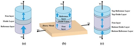
Figure 1.
Structure of a (a) 2-terminal STT PMA MTJ. (b) 3-terminal SOT PMA MTJ. (c) 2-terminal s-PMA DMTJ.
One of the most significant attributes of MTJs is their non-volatile behavior, which allows them to retain stored data for many years without requiring a continuous power supply [25]. This makes MTJs highly suitable for memory applications, where long-term data retention is essential. The operating principle of an MTJ is based on the relative alignment of the magnetization directions in the fixed and free layers. When the magnetizations of both ferromagnetic layers are aligned in the same direction, the MTJ exhibits low electrical resistance, a state known as the parallel state (P). Conversely, when the magnetizations are aligned in opposite directions, the MTJ exhibits high resistance, referred to as the anti-parallel state (AP). These two states, parallel and anti-parallel, correspond to the binary data storage states in memory applications. The difference in resistance between the P and AP states is quantified by tunnel magnetoresistance (TMR), a key parameter that defines the MTJ’s performance, given by Equation (1). TMR is calculated as the relative change in resistance between these two states and is a critical factor in determining the efficiency and reliability of MTJs in practical applications. The ability to precisely control and manipulate TMR in MTJs has led to their widespread use in spintronic devices, where they serve as the fundamental building blocks for non-volatile memory, logic circuits, and other advanced technologies that rely on the interplay of magnetic and electronic properties.
2.2. Hybrid MOS/MTJ Logic Structure
Figure 2 illustrates a hybrid MOS/MTJ structure designed within a logic-in-memory architecture, offering a sophisticated approach to integrating non-volatile memory with logic operations [5]. This hybrid structure comprises three main components: a sensing amplifier, a volatile and non-volatile logic structure, and a writing circuit dedicated to programming the non-volatile devices. This design leverages the strengths of both MOS transistors and MTJs to enhance the efficiency and functionality of the circuit, making it particularly suitable for applications requiring low-power, high-performance, and non-volatile data storage. The operation of this hybrid structure is influenced by both the data stored in the non-volatile logic elements and the input sequence provided to the NMOS logic structure. The interplay between these components determines the circuit’s overall output, enabling complex logic functions to be performed directly within the memory array, a key feature of logic-in-memory architectures. This integration reduces the need for extensive data movement between separate memory and processing units, thereby enhancing computational speed and energy efficiency.
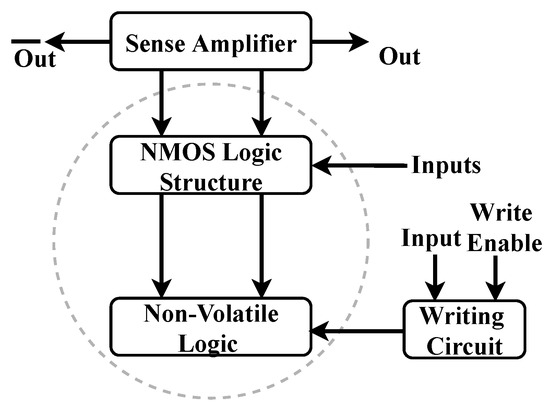
Figure 2.
Overview of MOS/MTJ hybrid logic structure.
The writing circuit plays a crucial role in this architecture by allowing specific bits to be written into the non-volatile logic. This is particularly important when utilizing MTJs as the non-volatile logic elements. For 2-terminal STT-MTJs, data is written by passing a charge current through the MTJ stack, which alters the magnetization state of the free layer, thereby changing the stored data. The STT effect is a well-established mechanism for switching the magnetic state, offering a reliable method for non-volatile data storage with low power consumption. In contrast, when employing a 3-terminal SOT-MTJ, the writing process becomes more complex. In this case, a larger charge current is directed through a metal layer positioned below the MTJ stack to induce the SOT effect, which switches the magnetization of the free layer. Simultaneously, a smaller charge current passes through the MTJ stack itself, contributing to the spin-transfer torque effect. This dual-current approach allows for more efficient and reliable switching of the MTJ, combining the benefits of both SOT and STT mechanisms. The writing circuit’s versatility is further demonstrated by its ability to write data to one or two MTJs connected in series. This is achieved using a four-transistor writing circuit, which provides precise control over the current flow and switching events within the MTJ structure [22,26]. By carefully managing the currents and voltages applied to the MTJs, the writing circuit ensures that the correct data is reliably stored in the non-volatile logic elements, making the hybrid MOS/MTJ structure a powerful tool for advanced memory and logic applications.
3. Proposed Work
Circuit Operation
The circuit illustrated in Figure 3a is a design based on a hybrid MOS/MTJ structure, combining the strengths of both technologies to achieve efficient sensing and logic operations. Central to the circuit’s operation is a pre-charge sense amplifier (PCSA), which plays a critical role in generating complementary outputs [27]. The use of a PCSA allows the circuit to effectively sense the resistance differences between the two MTJs, which arise due to the distinct magnetization directions of their free layers. This difference in resistance is key to the circuit’s ability to distinguish between logic states, enabling accurate data processing and storage.
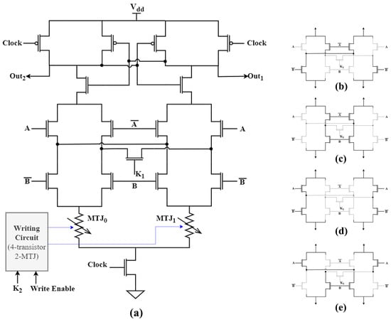
Figure 3.
(a) Schematic of the NPL circuit with complementary MTJs as non-volatile logic, four-transistor two-MTJ writing circuit, and pre-charge sense amplifier, and (b–e) NMOS logic circuit operation when is disabled for all potential combinations of A and B (00, 01, 10, and 11).
The operation of the circuit is divided into two distinct phases: the precharge phase and the evaluation phase. During the precharge phase, the Clock signal is held low, which activates the p-channel transistors within the PCSA. These transistors then charge both output nodes to the supply voltage, effectively precharging the circuit in preparation for the subsequent evaluation phase. This precharge phase is essential for ensuring that the circuit starts from a known state, allowing for precise and reliable sensing of the MTJ states in the following phase. Once the Clock signal transitions from 0 to 1, the circuit enters the evaluation phase. In this phase, the tail n-channel transistor of the PCSA is activated, initiating the discharge of the output nodes. As the outputs begin to discharge, the difference in resistance between the two MTJs becomes apparent. The MTJ with lower resistance (in the parallel state) allows faster discharge, leading to a rapid drop in voltage at the corresponding output node. Conversely, the output associated with the MTJ in the antiparallel state, which has higher resistance, discharges more slowly. The PCSA is designed with inverter pairs, which play a crucial role during the evaluation phase. As one of the outputs discharges completely to 0 V, the inverter pairs respond by driving the other output to the supply voltage. This mechanism ensures that the circuit generates a strong, complementary output signal, clearly distinguishing between the two possible states of the MTJs. The use of inverters in the PCSA not only amplifies the differential signal but also contributes to the robustness and speed of the circuit’s operation.
To facilitate the writing of states to the MTJs, the circuit incorporates a 4-transistor, 2-MTJ-based writing circuit. This writing circuit is responsible for programming the magnetic state of the MTJs, effectively setting the logic state that the circuit will subsequently sense and process. The writing operation is controlled by the signal, which is gated by the Write Enable signal. The signal remains inactive unless the Write Enable signal is asserted, preventing accidental or unauthorized writing to the MTJs.
To understand how the circuit functions across different input and key combinations, Table 1 provides a detailed listing of the resistances encountered in each branch of the PCSA. These resistances, determined by the on-resistance () of the MOS transistors and the specific states of the MTJs, play a crucial role in the circuit’s behavior during the evaluation phase. The width of the NMOS transistor connected to the input has been increased to minimize its resistance, thereby reducing its impact on output signals. All other NMOS transistors retain their default dimensions as per the TSMC 65 nm technology node. The width of the PMOS transistors remains consistent at 2.5 times that of the NMOS transistors. During the evaluation phase, the circuit distinguishes between the two branches of the PCSA based on their resistance levels. Since the transistors in the NMOS logic circuit have identical dimensions, in most cases shown in Table 1, the MTJ state determines the output of the PCSA. The branch with lower total resistance discharges to 0 V more quickly, while the branch with higher resistance discharges more slowly. These resistance values are governed by the P or AP state of the MTJs. This differential discharge process is essential for the circuit’s ability to generate complementary output signals. As one output node discharges rapidly, the associated inverter pairs within the PCSA drive the other output node high, resulting in a clear and distinct logic state. The delay in pulling down the PCSA output to 0 V depends on the resistance of each branch. However, this delay can be controlled by adjusting the dimensions of the respective transistors if necessary. Since the same circuit performs multiple operations, to reduce overall delay, only the width of the tail transistors can be increased to allow better current flow. Figure 3b–e further illustrate the behavior of NMOS logic circuitry when is set to 0 for all potential combinations of A and B (00, 01, 10, and 11). The circuit’s flexibility in executing various logic operations is one of its standout features. By adjusting the applied keys, specifically and , the circuit can perform all one- and two-input Boolean logic functions, including fundamental operations like AND, OR, NAND, NOR, XOR, and XNOR. The versatility of the circuit is further demonstrated in Table 2, which outlines the specific logic operations achieved at the output terminals based on the resistance values provided in Table 1. This table serves as a comprehensive guide to the circuit’s functionality, showing how different key combinations translate into specific logic operations.

Table 1.
Resistance offered by NMOS logic structure and MTJs to left and right branch of PCSA.
Table 2.
NPL circuit Operation with certain inputs and key combinations.
Beyond basic logic functions, the circuit’s design also allows it to perform more complex arithmetic operations. For instance, when the input carry is applied to key , the NPL circuit is capable of generating both the sum and carry outputs of a full adder (FA). This capability is particularly valuable in arithmetic logic units (ALUs), where efficient and reliable addition operations are essential. The ability to seamlessly integrate these arithmetic functions into the same circuit that performs Boolean logic operations highlights the circuit’s versatility and potential for use in a wide range of applications, from basic logic processing to complex computational tasks.
4. Results and Discussion
4.1. Analytical Results
The circuit operation is validated using the Cadence Spectre simulator, incorporating all MTJ configurations illustrated in Figure 1. For performance evaluation, Verilog-A-based MTJ behavioral models are integrated with the TSMC 65 nm CMOS technology node. The key parameters influencing MTJ behavior—such as device dimensions, temperature, and TMR—are summarized in Table 3. These parameters are carefully chosen to reflect typical operating conditions and to evaluate the circuit’s functionality under diverse scenarios. All simulations are conducted at 300 K using circular-shaped MTJs, known for their superior thermal stability and data retention.
Table 3.
Parameters of MTJ used for analytical modeling.
Although the proposed circuit is compatible with various MTJ designs, this study primarily concentrates on the STT-MTJ. The three investigated MTJ types differ mainly in their switching mechanisms and scaling behavior. The STT-MTJ employs perpendicular magnetic anisotropy, achieving reduced switching current through subvolume activation while maintaining thermal stability at around the 40 nm scale. The SOT-MTJ introduces a heavy metal layer that generates additional spin current via the spin-Hall effect, enabling faster switching and improved energy efficiency. In contrast, the sub-10 nm sPMA-DMTJ leverages a thicker free layer and shape anisotropy to preserve thermal stability and low switching current at nanoscale dimensions, albeit with higher resistance. Each configuration therefore offers distinct trade-offs among energy efficiency, switching speed, and scalability.
The output waveforms obtained from the circuit when using a two-terminal STT-MTJ are illustrated in Figure 4 and Figure 5. Figure 4 illustrates the circuit’s response to various input conditions, confirming its capability to perform the desired logic functions accurately. The key values are varied across all possible combinations, and their effect on the output logic has been recorded. Figure 5 demonstrates the circuit’s operation as an FA when the carry input is applied at . The results indicate that the same circuit can generate both the Sum and Carry outputs effectively. The obtained results, as presented in these figures, align closely with the expected behavior outlined in Table 2. The consistency between the simulated waveforms and the theoretical predictions underscores the accuracy of the circuit’s design and its effectiveness in implementing non-volatile logic operations. Additionally, other MTJ structures exhibited similar behavior with the specified inputs. The successful operation of the circuit across different MTJ types, especially under challenging sub-10nm conditions, highlights its versatility and potential for use in a wide range of advanced electronic applications.
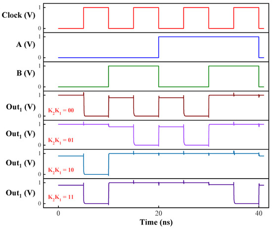
Figure 4.
Analytical input and output plots of the NPL circuit with specific key values.
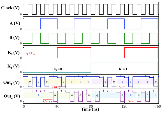
Figure 5.
Simulated waveform of the NPL circuit behaving as a full adder.
In the output of the circuit at , as illustrated in Figure 4, the response for all key combinations exhibits a distinctive behavior. Since both output nodes are pre-charged to the supply voltage, the rise time during the evaluation phase is effectively considered zero when measuring the output. To gain deeper insights into the circuit’s operation, a timing analysis was conducted to measure the delay between input and output, as well as the fall time at the output. The fall time indicates how quickly the circuit’s output can be pulled to the ground. For different operations using STT-MTJ devices, the observed delay and fall times are summarized in Table 4. Further analysis confirmed that increasing the width of the NMOS tail transistor can reduce both the delay and fall time. A wider NMOS tail transistor allows the output nodes to discharge more rapidly, improving the circuit’s overall speed. Despite these optimizations, the circuit’s power consumption remains low, at only a few microwatts, with minimal variation across all operations.
Table 4.
Maximum delay and fall time observed for various operations.
4.2. Security Aspects
The non-volatile nature of MTJs presents a unique opportunity to both prevent and detect tampering in integrated circuits. By leveraging this property, a circuit can be designed to perform multiple operations, thereby concealing its true functionality or layout after fabrication. Attackers in the fabrication facility are effectively prevented from introducing malicious modifications, as they are unaware of how certain logic blocks behave. This dynamic functionality can be achieved by altering the state of MTJs using predefined key values, making it possible to modify the operation or functionality of gates as needed. Once the fabrication process is complete, the MTJ state can be permanently set to ensure the circuit operates as intended, adding a layer of post-manufacturing security.
One of the key advantages of this approach is that the timing characteristics for different logic operations are similar, which further complicates any attempt at tampering. For instance, the fall time and delay for operations like NAND, OR, and XNOR are almost indistinguishable, with delays such as 14 ps, and only minor variations in other parameters. This similarity makes it difficult for an attacker to identify the correct operation of the circuit using timing-based side-channel attacks, as there are no obvious differences to exploit. The delay characteristics are governed by the resistance of the left and right branches of the PCSA. Further optimization of the circuit to achieve uniform timing characteristics across all operations is beyond the scope of the present work.
The layout of the NPL circuit implemented using the TSMC 65nm MOS technology node, as shown in Figure 6, further demonstrates the symmetry of the design. This symmetry is critical because it means that the same physical layout can execute all possible operations depending on the unique key values. Consequently, this approach eliminates the need for additional camouflage at the layout level, as the uniformity of the layout provides inherent protection against reverse engineering. In essence, the proposed structure serves as a form of logic locking or circuit obfuscation without the need to incorporate extra components, unlike conventional logic locking techniques.
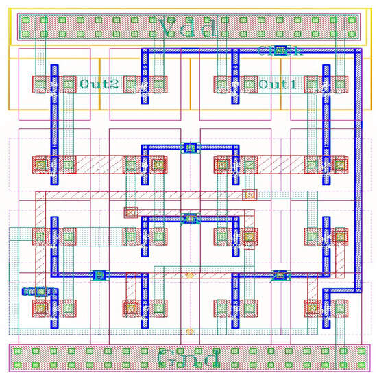
Figure 6.
Layout of the NPL circuit.
In addition to security against tampering, IP protection techniques such as watermarking and fingerprinting can be integrated into this design to obfuscate authorship details or include unique identifiers without affecting circuit performance [10]. The operational process of the logic circuit utilizing NPL for enhanced watermarking and fingerprinting, as illustrated in Figure 7, reveals several mechanisms allowing these security features to be effectively integrated and managed without compromising circuit performance. In the depicted design, each input (A, B, C) is routed through individual NPL units, which are based on MTJ devices. These units possess programmable, non-volatile states, meaning that specific “keys” or configuration bits can be set to encode unique identifiers or watermarks into the hardware itself. The final output is then determined by the programmed states of the NPL blocks.
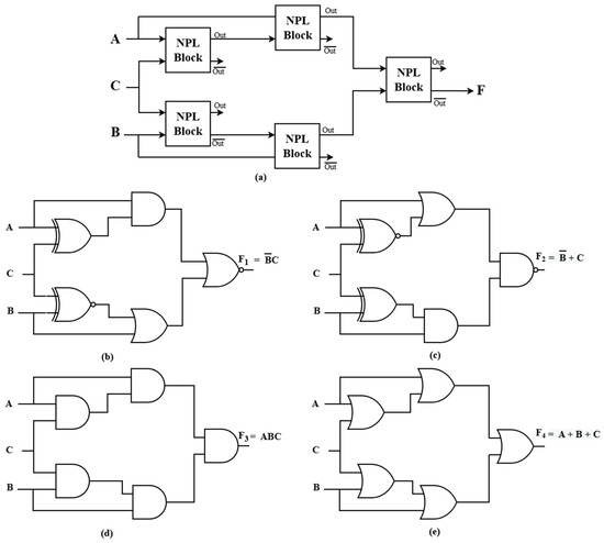
Figure 7.
(a) Logic circuit utilizing NPL for enhanced watermarking and fingerprinting, (b–e) Examples of various configurations of the NPL-based logic circuit.
In watermarking, the NPL can be configured such that certain programmed states remain hidden under normal operation (with fixed keys), while only under specific key changes does the circuit reveal its embedded watermark or IP identifier. This operational concealment is supported by the stable MTJ properties, which prevent inadvertent state changes and guarantee fidelity of the embedded identifier until a deliberate “reveal” is initiated. For fingerprinting, unique keys specific to the authorized user or design house can be programmed into the NPL blocks. Upon validation—by toggling the corresponding key states—the fingerprint becomes observable in the output without disrupting normal logic function or performance. This feature is valuable for secure authorship or ownership assertion. Figure 7 demonstrates how such NPL-based design enables multiple logic functions to be implemented using reprogrammable logic gates. The NPL blocks can be dynamically programmed so the same circuit hardware selectively operates as different combinational functions depending on the programmed key settings. Initially, the embedded watermark or fingerprint remains locked and concealed, preserving circuit integrity and standard operation. When verification or IP assertion is needed, the keys can be altered to activate alternate modes that disclose the relevant watermark or fingerprint. The stability of spintronic MTJ elements ensures that watermarking/fingerprinting mechanisms cannot be tampered with unintentionally; only explicit programming commands can change their state and reveal hidden information. The multifunctional and programmable nature of these NPL logic circuits enables robust defense against counterfeiting, unauthorized modifications, and design piracy, while maintaining the high-speed and low-power performance characteristic of MTJ devices.
Table 5 provides a valuable foundation for understanding the attempts made in developing spin-based polymorphic gates. The research summarized in this table demonstrates the potential of spintronic devices to revolutionize computing architectures by offering novel approaches to reconfigurable logic. Although several efforts have explored different spintronic devices for this purpose, the proposed approach offers distinct advantages. The same circuit can operate with various MTJ structures, enabling multiple logic operations without the need for separate circuits. A single design performs all one- and two-input Boolean logic functions. Furthermore, the symmetrical layout enhances the overall effectiveness of this approach in hardware security. Various other technologies have also been explored in the literature for achieving polymorphic behavior, such as memristors, multi-gate FETs, and 2D materials-based devices; however, discussion of these technologies is currently beyond the scope of this work. Future research efforts should focus on further enhancing the flexibility, efficiency, and scalability of these devices to meet the demands of emerging applications.
Table 5.
Different reconfigurable logic utilizing spintronic devices.
5. Conclusions
The proposed Non-volatile Polymorphic Logic circuit demonstrates the potential to obfuscate circuit functionality, making it challenging for attackers to compromise. analytical results confirm the feasibility and efficiency of the proposed approach, highlighting its ability to perform various boolean operations while maintaining similar timing characteristics. The symmetric circuit layout further strengthens security by providing post-manufacturing protection from reverse engineering to detect functionality. This work contributes to the development of more resilient and secure integrated circuits, addressing the growing concerns associated with hardware trojans and intellectual property theft while also paving the way for further optimization in power, area, and scalability for advanced nodes. Integrating MTJ-based designs into large-scale arrays or SoCs poses challenges including high write energy, device variability affecting reliability, and increasing complexity in key management. Nevertheless, with ongoing advancements in device performance and integration methods, practical deployment of MTJ-based polymorphic logic in secure, scalable systems is envisioned to be achievable in the future.
Author Contributions
Conceptualization, R.K., Y.S. and A.K.G.; Formal analysis, R.K. and Y.S.; Investigation, A.K.G.; Methodology, R.K. and A.K.G.; Supervision, A.K.G.; Validation, R.K. and Y.S.; Writing—original draft, R.K. and Y.S.; Writing—review and editing, R.K., Y.S. and A.K.G. All authors have read and agreed to the published version of the manuscript.
Funding
This research received no external funding.
Data Availability Statement
All data supporting the findings of this study are included in the article. Additional details may be obtained from the authors upon reasonable request.
Conflicts of Interest
The authors declare no conflicts of interest.
References
- Semiconductor Industry Association. Available online: https://www.semiconductors.org/ (accessed on 6 September 2025).
- Hu, W.; Chang, C.H.; Sengupta, A.; Bhunia, S.; Kastner, R.; Li, H. An Overview of Hardware Security and Trust: Threats, Countermeasures, and Design Tools. IEEE Trans. Comput.-Aided Des. Integr. Circuits Syst. 2021, 40, 1010–1038. [Google Scholar] [CrossRef]
- Rajendran, J.; Karri, R.; Wendt, J.B.; Potkonjak, M.; McDonald, N.; Rose, G.S.; Wysocki, B. Nano Meets Security: Exploring Nanoelectronic Devices for Security Applications. Proc. IEEE 2015, 103, 829–849. [Google Scholar] [CrossRef]
- Ghosh, S. Spintronics and Security: Prospects, Vulnerabilities, Attack Models, and Preventions. Proc. IEEE 2016, 104, 1864–1893. [Google Scholar] [CrossRef]
- Matsunaga, S.; Hayakawa, J.; Ikeda, S.; Miura, K.; Endoh, T.; Ohno, H.; Hanyu, T. MTJ-based nonvolatile logic-in-memory circuit, future prospects and issues. In Proceedings of the 2009 Design, Automation & Test in Europe Conference & Exhibition, Nice, France, 20–24 April 2009; pp. 433–435. [Google Scholar] [CrossRef]
- Wang, X.; Yang, J.; Zhao, Y.; Jia, X.; Qu, G.; Zhao, W. Hardware Security in Spin-based Computing-in-memory: Analysis, Exploits, and Mitigation Techniques. ACM J. Emerg. Technol. Comput. Syst. 2020, 16, 37. [Google Scholar] [CrossRef]
- Divyanshu, D.; Lone, A.H.; Tang, M.; Florica, C.; Amara, S.; Setti, G. Hardware Aware Polyalphabetic Cipher Design Using Spin-Orbit Torque Controlled Spintronic Devices. IEEE Trans. Circuits Syst. II Express Briefs 2025, 72, 963–967. [Google Scholar] [CrossRef]
- Perach, B.; Kvatinsky, S. An Asynchronous and Low-Power True Random Number Generator using STT-MTJ. In Proceedings of the 2020 IEEE International Symposium on Circuits and Systems (ISCAS), Online, 10–21 October 2020; p. 1. [Google Scholar] [CrossRef]
- Divyanshu, D.; Kumar, R.; Khan, D.; Amara, S.; Massoud, Y. FSM Inspired Unconventional Hardware Watermark Using Field-Assisted SOT-MTJ. IEEE Access 2023, 11, 8150–8158. [Google Scholar] [CrossRef]
- Kumar, R.; Divyanshu, D.; Khan, D.; Amara, S.; Massoud, Y. Polymorphic Hybrid CMOS-MTJ Logic Gates for Hardware Security Applications. Electronics 2023, 12, 902. [Google Scholar] [CrossRef]
- Stoica, A.; Zebulum, R.; Keymeulen, D. Polymorphic Electronics. In Evolvable Systems: From Biology to Hardware; Liu, Y., Tanaka, K., Iwata, M., Higuchi, T., Yasunaga, M., Eds.; Springer: Berlin/Heidelberg, Germany, 2001; pp. 291–302. [Google Scholar]
- Rakheja, S.; Kani, N. Polymorphic spintronic logic gates for hardware security primitives — Device design and performance benchmarking. In Proceedings of the 2017 IEEE/ACM International Symposium on Nanoscale Architectures (NANOARCH), Newport, RI, USA, 25–26 July 2017; pp. 131–132. [Google Scholar] [CrossRef]
- Zhao, W.; Belhaire, E.; Chappert, C.; Mazoyer, P. Spin transfer torque (STT)-MRAM–based runtime reconfiguration FPGA circuit. ACM Trans. Embed. Comput. Syst. 2009, 9, 14. [Google Scholar] [CrossRef]
- Roohi, A.; DeMara, R.F. PARC: A Novel Design Methodology for Power Analysis Resilient Circuits Using Spintronics. IEEE Trans. Nanotechnol. 2019, 18, 885–889. [Google Scholar] [CrossRef]
- Angizi, S.; He, Z.; Chen, A.; Fan, D. Hybrid Spin-CMOS Polymorphic Logic Gate with Application in In-Memory Computing. IEEE Trans. Magn. 2020, 56, 1–15. [Google Scholar] [CrossRef]
- Zhang, Y.; Yan, B.; Wu, W.; Li, H.; Chen, Y. Giant spin hall effect (GSHE) logic design for low power application. In Proceedings of the 2015 Design, Automation & Test in Europe Conference & Exhibition (DATE), Grenoble, France, 9–13 March 2015; pp. 1000–1005. [Google Scholar]
- Patnaik, S.; Rangarajan, N.; Knechtel, J.; Sinanoglu, O.; Rakheja, S. Advancing hardware security using polymorphic and stochastic spin-hall effect devices. In Proceedings of the 2018 Design, Automation & Test in Europe Conference & Exhibition (DATE), Dresden, Germany, 19–23 March 2018; pp. 97–102. [Google Scholar] [CrossRef]
- Kumar, S.D.; Thapliyal, H. Security evaluation of MTJ/CMOS circuits against power analysis attacks. In Proceedings of the 2017 IEEE International Symposium on Nanoelectronic and Information Systems (iNIS), Bhopal, India, 18–20 December 2017; IEEE: Piscataway, NJ, USA, 2017; pp. 117–122. [Google Scholar]
- Nisar, A.; Zahoor, F.; Thakker, S.S.; Das, K.K.; Maitra, S.; Kaushik, B.K.; Chattopadhyay, A. SOT-MTJ Based Non-Volatile Flip-Flop with In-Memory Randomness for Application in Grain Stream Ciphers. IEEE Access 2025, 13, 34677–34686. [Google Scholar] [CrossRef]
- Chowdhury, M.A.; Hossain, M.; Mastrangelo, C.; DeMara, R.F.; Salehi, S. S-Tune: SOT-MTJ manufacturing parameters tuning for securing the next generation of computing. Front. Electron. 2024, 5, 1409548. [Google Scholar] [CrossRef]
- Adel, M.J.; Rezayati, M.H.; Moaiyeri, M.H.; Amirany, A.; Jafari, K. A robust deep learning attack immune MRAM-based physical unclonable function. Sci. Rep. 2024, 14, 20649. [Google Scholar] [CrossRef] [PubMed]
- Zhang, Y.; Yan, B.; Kang, W.; Cheng, Y.; Klein, J.O.; Zhang, Y.; Chen, Y.; Zhao, W. Compact Model of Subvolume MTJ and Its Design Application at Nanoscale Technology Nodes. IEEE Trans. Electron Devices 2015, 62, 2048–2055. [Google Scholar] [CrossRef]
- Wang, Z.; Zhao, W.; Deng, E.; Klein, J.O.; Chappert, C. Perpendicular-anisotropy magnetic tunnel junction switched by spin-Hall-assisted spin-transfer torque. J. Phys. D Appl. Phys. 2015, 48, 065001. [Google Scholar] [CrossRef]
- Wang, H.; Kang, W.; Zhang, Y.; Zhao, W. Modeling and Evaluation of Sub-10-nm Shape Perpendicular Magnetic Anisotropy Magnetic Tunnel Junctions. IEEE Trans. Electron Devices 2018, 65, 5537–5544. [Google Scholar] [CrossRef]
- Chun, K.C.; Zhao, H.; Harms, J.D.; Kim, T.H.; Wang, J.P.; Kim, C.H. A Scaling Roadmap and Performance Evaluation of In-Plane and Perpendicular MTJ Based STT-MRAMs for High-Density Cache Memory. IEEE J. Solid-State Circuits 2013, 48, 598–610. [Google Scholar] [CrossRef]
- Zhang, Y.; Zhao, W.; Kang, W.; Deng, E.; Klein, J.O.; Revelosona, D. Current-Induced Magnetic Switching for High-Performance Computing. In Spintronics-Based Computing; Zhao, W., Prenat, G., Eds.; Springer International Publishing: Cham, Switzerland, 2015; pp. 1–51. [Google Scholar] [CrossRef]
- Kim, J.; Ryu, K.; Kang, S.H.; Jung, S.O. A Novel Sensing Circuit for Deep Submicron Spin Transfer Torque MRAM (STT-MRAM). IEEE Trans. Very Large Scale Integr. (VLSI) Syst. 2012, 20, 181–186. [Google Scholar] [CrossRef]
Disclaimer/Publisher’s Note: The statements, opinions and data contained in all publications are solely those of the individual author(s) and contributor(s) and not of MDPI and/or the editor(s). MDPI and/or the editor(s) disclaim responsibility for any injury to people or property resulting from any ideas, methods, instructions or products referred to in the content. |
© 2025 by the authors. Licensee MDPI, Basel, Switzerland. This article is an open access article distributed under the terms and conditions of the Creative Commons Attribution (CC BY) license (https://creativecommons.org/licenses/by/4.0/).