Abstract
The silicon nitride (SiN) platform offers a low-loss solution for photonic integrated circuits (PICs). The bent waveguide represents one of the primary sources of propagation loss in such integrated systems. In this work, we present a comprehensive review of recent advances in SiN bent waveguide technologies. We propose a low-loss SiN bent waveguide design integrated with modified Hermite curves. We adopt a waveguide geometry of 800 nm × 300 nm in the simulations, with the material refractive index derived from the LPCVD process. Simulations conducted at a wavelength of 1311 nm reveal that the proposed bends exhibit bending losses of 0.076 dB, 0.021 dB, 0.0055 dB, and 0.0012 dB per 90° bend, corresponding to bending radii of 15 μm, 20 μm, 25 μm, and 30 μm, respectively. Furthermore, the fabrication tolerance and wavelength dependence of the proposed design are systematically investigated to verify its practical applicability.
1. Introduction
Silicon nitride (SiN) has emerged as a highly promising material for photonic applications, owing to its broad optical transparency window, ultra-low propagation loss, moderate Kerr nonlinearity, excellent high-power handling capability, superior thermal stability, and compatibility with the complementary metal-oxide-semiconductor (CMOS) process [1,2]. SiN exhibits negligible two-photon absorption at communication wavelengths—a nonlinear effect that can act as a limiting factor in silicon optical waveguides. This property enables SiN devices to handle higher optical power, establishing it as the preferred platform for nonlinear applications such as frequency comb generation [2]. Unlike silicon, which becomes opaque at wavelengths below ~1.1 μm, SiN maintains high optical transparency over an exceptionally broad wavelength range, spanning from the visible spectrum to the mid-infrared region. This unique characteristic renders it an ideal platform for applications beyond traditional communication bands, such as displays, biophotonics, mid-infrared sensing [3].
SiN optical waveguides are renowned for their extremely low propagation loss, which now routinely falls within the decibel-per-meter (dB/m) range [4]. This performance is mainly attributed to the high-quality SiN thin films deposited via techniques such as LPCVD and the relatively low refractive index contrast between SiN (~2.0) and silicon dioxide (~1.5)—an attribute that reduces scattering loss induced by sidewall roughness. Recent demonstrations have reported losses as low as 0.045 dB/m [5] and 0.034 dB/m [6].
However, the lower refractive index contrast of SiN compared to silicon-on-insulator (SOI) necessitates a larger bending radius, which in turn limits the integration density of SiN PICs [7]. Therefore, developing a design methodology for compact, low-loss bent waveguides is of great significance for advancing PIC implementations on the SiN platform.
To date, The O-band has become the preferred solution for short-reach optical communications, especially for applications in data centers [8]. For example, 1.6-Tb/s transmission over 10 km in the O-band using 400-Gb/s/lane spatial division multiplexing (SDM) channels has been demonstrated, highlighting its critical role in high-speed data transfer [8]. However, to the best of our knowledge, the minimum bending radius for the O-band SiN waveguide is 30 μm and the loss is 0.004 dB/90°, which has been realized through an adiabatic design [9]. As for the low-loss O-band SOI waveguide, the bending radius can be reduced to 5 μm with a loss of 0.06 dB/90° [10]. This significant disparity underscores the critical need to investigate the trade-offs between compactness and propagation loss in O-band SiN bent waveguides. Despite its importance, relatively little research has been conducted on SiN bent waveguides operating at the O-band.
In this paper, we first briefly analyze the bending loss mechanism and review the state-of-the-art of SiN bent waveguides. Then we propose a novel bending design approach to realize compact, low-loss O-band SiN waveguides with enhanced wavelength insensitivity. Numerical simulations show bending loss of 0.076 dB, 0.021 dB, 0.0055 dB, and 0.0012 dB per 90° at radii of 15 μm, 20 μm, 25 μm, and 30 μm, respectively. We compare their performance with circular, and other advanced bending techniques, and analyze the impact of fabrication process errors.
2. Low Loss SiN Waveguide Bend
2.1. The SiN Material
Currently, there are two mainstream techniques for depositing SiN thin films: low-pressure chemical vapor deposition (LPCVD) and plasma-enhanced chemical vapor deposition (PECVD). Both have been widely applied in practice, and each possesses distinct technical characteristics [1].
Silicon nitride thin films prepared via LPCVD exhibit a relatively fixed refractive index, which ensures high performance stability for optical devices based on it. Additionally, these films contain extremely low levels of hydrogen bonds, endowing them with excellent low-loss properties. However, LPCVD has significant limitations. For one thing, its deposition process requires a high-temperature environment (900~1100 °C), making it incompatible with the silicon photonics process platform with doping process for modulation and detection functions. For another, the high-purity silicon nitride thin films produced by LPCVD are prone to stress-related issues, and the film will crack when grown to a certain thickness [7]. Thus, high thickness (>400 nm) remains a core challenge for LPCVD-based silicon nitride waveguides. A solution to this problem is the adoption of the damascene process, which was proposed by the Swiss Federal Institute of Technology Lausanne (EPFL) [11]. This process embeds silicon nitride (SiN) into silica trenches by combining etching and chemical mechanical polishing (CMP) techniques, and it can effectively address the stress issue. However, it suffers from two main drawbacks: the thickness and width of the SiN waveguide are difficult to precisely control; in addition, the CMP process applied to large-area SiN regions results in a dishing effect, where the concentrated pressure exerted by the polishing head leads to over-polishing, causing a central depression of 10–20 nm [12].
In contrast, PECVD silicon nitride waveguides offer notable integration advantages. They can be seamlessly compatible with the silicon photonics platform, enabling the construction of multi-layer optical waveguide structures. Meanwhile, film stress can be effectively adjusted by regulating process parameters, allowing the thickness of PECVD silicon nitride waveguides to 800 nm [13]. Nevertheless, PECVD also has prominent shortcomings. The silicon nitride thin films it produces typically contain more hydrogen bonds, which induce substantial absorption loss in waveguides. This loss is difficult to further reduce through conventional methods. While high-temperature annealing can mitigate this loss by decreasing hydrogen bond content (when temperature conditions permit), the transmission loss of PECVD silicon nitride waveguides remains significantly higher than that of LPCVD-prepared counterparts [14].
2.2. Bending Loss
Bending loss in waveguides mainly includes propagation loss, radiation loss, and mode conversion loss [15,16]. The propagation loss originates from absorption and scattering caused by material properties, growth defects, and fabrication imperfections. The surface scattering becoming the dominant factor after optimizing waveguide growth quality [16]. Radiation loss is mainly caused by waveguide bending, which weakens the confinement of light, resulting in leakage into the cladding [17]. This can be alleviated by optimizing the design or increasing the bending radius. The mode conversion loss arises from mode field mismatch at the junction of straight and bent waveguides, especially due to distorted mode profiles caused by sudden curvature changes, and can be reduced by designing structures with gradually varying curvature [18].
2.3. State-of-the-Art in SiN Bent Waveguides
Here, we briefly review the state-of-the-art of bent waveguides. Table 1 summarizes the results of SiN waveguide bends.
In 2016, the IMEC team proposed a low-loss SiN bent waveguide for the visible band by introducing an offset at the interface between the bent and the straight waveguides—with the configuration illustrated in Figure 1a. This waveguide was fabricated via the PECVD process. A bending loss of 0.215 dB/90° was achieved at a radius of 5 μm, representing a reduction of 0.4 dB/90° compared to that of conventional bent waveguides [19].
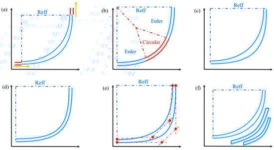
Figure 1.
Schematic diagram of the selected SiN bent waveguide design method. (a) Bent waveguide with offset progressive contour. (b) Partial Euler waveguide bends. (c) Advanced bends. (d) Euler spiral. (e) Modified Bezier bent waveguide (f) Inverse-designed bends.
In 2019, the team from Austrian Institute of Technology GmbH conducted a detailed analysis of various loss mechanisms of partially Euler-bent silicon nitride at a wavelength of 850 nm. They proposed a silicon nitride bent waveguide based on a partial Euler-bend geometry, as shown in Figure 1b. This structure optimized the transmission performance of small-radius optical waveguide bends and achieved a balance between the loss during the transition from the straight waveguide mode to the bent waveguide mode and the radiation loss of the bent waveguide mode. A bending loss of 0.007 dB/90° was achieved at a radius of 50 μm [20].
In 2020 and 2024, IMEC proposed a design method of advanced bends composed of width expansion and radius change at wavelengths of 850 nm and 1550 nm respectively, as shown in Figure 1c, and achieved extremely low bending losses through PECVD and LPCVD process methods respectively. Specifically, at a wavelength of 850 nm, the bending loss of a SiN waveguide with a radius of 15 μm decreases from 0.13 dB/90° for a conventional circular bends to 0.04 dB/90° [21]. And, at the wavelength of 1550 nm, the bending loss of a SiN waveguide bend with a radius of 25 μm was reduced from 0.048 dB/90° to 0.022 dB/90° [22].
In 2021, the team from Advanced Micro Foundry (AMF) proposed a so-called advanced waveguide bend based on the Euler spiral using a CMOS-compatible multi-layer PECVD SiN-on-SOI integration platform, as shown in Figure 1d. The curvature of this bend was designed to change linearly to reduce bending loss. The bending loss of SiN with a radius of 30 μm was reduced from 0.087 dB/90° for conventional circular bends to 0.037 dB/90° for the Euler bends [23].
In 2022, the team from Zhejiang University proposed a modified Bezier bend design for SiN PICs and validated its low-loss performance experimentally, with the configuration illustrated in Figure 1e. For a SiN bend with a bending radius of 12 µm, the measured bending loss was reduced to 0.32 dB per 90°—a significant improvement compared to 0.65 dB per 90° for conventional circular bends and 0.575 dB per 90° for traditional Bezier bends [24].
In 2025, the team from École de technologie supérieure (ÉTS) demonstrated the application of inverse design for realizing high-efficiency, compact bends in SiN waveguides, with a minimum bending radius of 6 µm (as illustrated in Figure 1f). These bends were specifically designed for the transverse electric (TE) polarization of single-mode waveguides. Devices were fabricated via electron-beam lithography (EBL), with the minimum feature size constrained to 160 nm to enhance compatibility with commercial CMOS foundries, and experimental results show that the free-form bends enabled by inverse design outperform conventional circular and Euler bends in terms of performance across four distinct footprint areas (ranging from 6 × 6 µm2 to 21 × 21 µm2). At bending radii of 6 µm, 11 µm, 16 µm, and 21 µm, the measured bending losses are 1.89 dB/90°, 0.18 dB/90°, 0.08 dB/90°, and 0.11 dB/90°, respectively [25].
In 2025, the TSMC team demonstrated an adiabatic SiN bent waveguide with PECVD and 65 nm process. The device exhibits a measured bending loss of 0.004 dB per 90° bend at 1311 nm, with a bending radius of 30 µm [9].

Table 1.
State-of-the-art in compact SiN bends with experimental demonstrations.
Table 1.
State-of-the-art in compact SiN bends with experimental demonstrations.
| Year/Ref. | Affiliation | Radius (µm) | Bending Loss (dB/90°) | Wavelength (nm) | Process | Waveguide Dimension (Width × Height) |
|---|---|---|---|---|---|---|
| 2016/[19] | IMEC | 3 | 1.403 | 638 | PECVD | 450 nm × 220 nm |
| 4 | 0.633 | |||||
| 5 | 0.215 | |||||
| 7 | 0.054 | |||||
| 10 | 0.034 | |||||
| 2019/[20] | AIT | 50 | 0.007 | 850 | NA | 680 nm × 160 nm |
| 2020/[21] | IMEC | 5 | 1.82 | 850 | PECVD | 600 nm × 300 nm |
| 10 | 0.25 | |||||
| 15 | 0.04 | |||||
| 20 | 0.01 | |||||
| 2021/[23] | AMF | 30 | 0.037 | 1550 | PECVD SiN on SOI | 1000 nm × 400 nm |
| 40 | 0.031 | |||||
| 50 | 0.023 | |||||
| 2022/[24] | ZJU | 8 | 1.225 | 1550 | LPCVD | 1200 nm × 400 nm |
| 10 | 0.525 | |||||
| 12 | 0.32 | |||||
| 2024/[22] | IMEC | 15 | 0.13 | 1550 | LPCVD | 1000 nm × 400 nm |
| 20 | 0.03 | |||||
| 25 | 0.025 | |||||
| 2025/[25] | ÉTS | 6 | 1.86 | 1550 | PECVD | 850 nm × 400 nm |
| 11 | 0.18 | |||||
| 16 | 0.08 | |||||
| 21 | 0.11 | |||||
| 2025/[9] | TSMC | 30 | 0.004 | 1311 | PECVD SiN on SOI | 800 nm × NA |
3. Device Structure and Design Method
3.1. Hermite Bend
Hermite curves find extensive applications in computer graphics and animation for defining the trajectories of moving objects—such as characters or vehicles—thereby ensuring a smooth and natural appearance to their motion [26].
Hermite curves are defined through Hermite interpolation, a method that ensures the continuity of higher-order derivatives at the connection points. This property is crucial for mitigating radiation loss and higher mode excitation in bent waveguides, thereby ensuring single-mode, low-loss transmission. A Hermite curve is parameterized by two endpoints and their corresponding tangent vectors. A schematic diagram of a Hermite curve bend, which is a third-order interpolation with two joints, is shown in Figure 2a. The expressions for the Hermite curve are as follows:
where P0 and P1 denote the starting and endpoints, respectively. While M0 and M1 represent their corresponding tangent vectors. The variable t is a parameter that traces the curve from the beginning (t = 0) to the end (t = 1). The Hermite curve is expressed as a linear combination of four basic functions and four weighting factors. As depicted in Figure 2a, a 90° Hermite bend can be formed by cascading two 45° Hermite bends, which implies that the parameters a0 and a1 are equal.
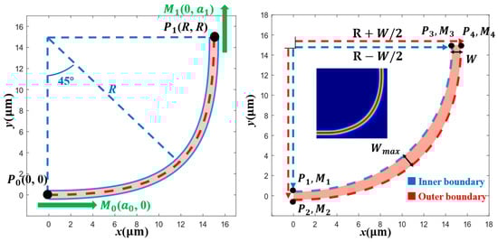
Figure 2.
(a) Hermite bend configuration and its design parameters. (b) Modified Hermite bend, design parameters and its electrical fields.
3.2. Modified Hermite Bend
We noticed that changing the width of a bent waveguide can effectively reduce losses [9,19,21,22,24,27]. This led us to the idea that by slowly changing the waveguide width based on the Hermite curve, the characteristics of bending losses can be improved. Upon its initial application in silicon photonic chips, the Hermite bend achieved exceptionally low losses and minimal mode excitation [28]. While Hermitian bends can effectively mitigate bending loss by adjusting tangential parameters, their performance is limited by a fixed width. To address this issue, improved Hermitian bends with variable widths can be constructed by introducing width variation. The graded-width design can effectively enhance the optical field confinement capability; an appropriate increase in width can raise the effective refractive index and mode confinement factor, thereby reducing the leakage of the optical field into the cladding [7,19].
For a specified bending radius R, the geometric configuration of the modified Hermite bend is constructed from two coupled Hermite curves rather than being defined by a single pair of start and end points (e.g., P0 and P1) for the entire waveguide path. Specifically, the two constituent Hermite curves take P1 and P2 as their respective starting points—corresponding to the two edge points at the initiation of the waveguide path—and P3 and P4 as their terminal points, which are the two edge points at the termination of the waveguide path. Notably, all these four key edge points (P1, P2, P3, P4) remain fixed for a given radius R. By employing the aforementioned method, two Hermite curves can be derived, as illustrated in Figure 2b, with their specific parameters detailed in Table 2. Here, W denotes the input waveguide width.
Table 2.
Modified Hermite bend parameters.
The precise geometry of the modified Hermite bend is determined by the boundary lines of the two Hermite bends depicted in the figure. For the inner boundary of the modified Hermite bend, with a radius of R − W/2, the governing equation can be expressed as:
For the modified Hermite bend outer boundary with a radius of R + W/2, the equation for the outer boundary can be expressed as:
As depicted in Figure 2, the waveguide width varies, reaching its maximum at the 45° mark. Owing to the structural symmetry of the bent waveguide at 45°, the parameters are related such that a1 = a3 and a2 = a4. Consequently, for a given radius, the optimization process for achieving minimum loss is simplified to finding the optimal values for only two parameters, a1 and a2.
4. Simulation Results
We have designed 90° bending waveguides on a 300 nm LPCVD SiN platform with effective radii of 15 μm, 20 μm, 25 μm, and 30 μm, each having an input width of 0.8 μm. This specific width was chosen to ensure the waveguide operates in a single-mode regime. The platform includes a bottom buried oxide layer, a top silicon oxide cladding, and a silicon nitride core with a refractive index of 2.0.
For the modified Hermite bend structure, the optimal configuration corresponding to minimum bending loss can be achieved by adjusting parameters a1 and a2. To determine the ideal values of these two parameters, we conducted simulation analyses using the three-dimensional finite-difference time-domain (3D-FDTD) method targeting the quasi-fundamental transverse electric (quasi-TE) mode, combined with the particle swarm optimization (PSO) algorithm. The two parameters a1 and a2 range from 15 to 80, with the key constraint condition during optimization set as a1 ≦ a2. A total of 100 iterations were performed in this optimization, and the iteration process is presented in the figure, with all iterations achieving convergence. The only figure of merit (FOM) for evaluating the bent structure is insertion loss (IL). The PSO results for the three bent structures with different radii are illustrated in Figure 3a.
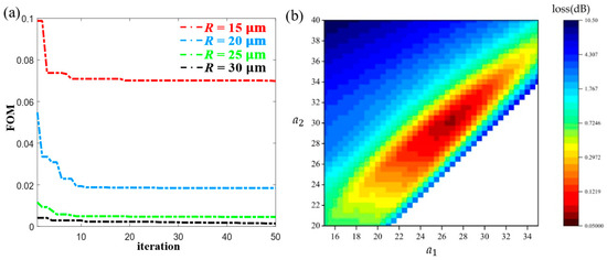
Figure 3.
(a) PSO-based optimization of modified silicon Hermite bends for radii of 15 μm, 20 μm, 25 μm, and 30 μm. (b) 2D Heat map of Sweep Results of modified silicon Hermite bends for radii of 15 μm.
To verify the reliability of the PSO algorithm and intuitively demonstrate the parameter optimization process, we employed a parameter sweeping method for the auxiliary search of the optimal a1 and a2 values for the structure with a radius of 15 μm. The sweeping results are depicted as a two-dimensional (2D) heat map in Figure 3b. When a2 is significantly smaller than a1, the outer boundary of the bent structure intersects with the inner boundary, resulting in structural failure and a sharp increase in loss. Therefore, the results corresponding to these invalid parameters in the heat map have been excluded. As shown in Figure 3b, the sweeping results are in perfect agreement with the PSO results listed in Table 3, which further confirms the accuracy of the algorithm. The optimal parameter values of a1 and a2 for the modified Hermite bend, as well as the comparison results with the bending loss of the circular bend, are all summarized in Table 3, and the corresponding schematic diagrams of the structures are presented in Figure 4.
Table 3.
Optimal values of bend parameters of modified Hermite bends and comparison of losses with circular bends.
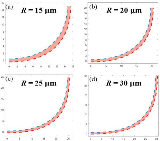
Figure 4.
The structure of the modified Hermite bend when (a) R = 15 µm, (b) R = 20 µm, (c) R = 25 µm and (d) R = 30 µm.
To rigorously validate the performance of the proposed modified Hermite bend and ensure the fairness of the comparison, two sets of comparative simulations were conducted using 3D-FDTD under identical mesh precision and boundary settings. The first set benchmarks the proposed design against the conventional Hermite bend (both optimized via systematic scanning) and includes a comparison with the standard circular bend, with the results presented in Figure 5a. The second set contrasts the proposed structure with state-of-the-art alternatives—specifically the advanced bend [22] and the modified Bezier bend [24]—all of which were optimized using the same PSO algorithm to ensure algorithmic consistency; the corresponding spectral responses are illustrated in Figure 5b. For a quantitative assessment, the simulated insertion losses of the aforementioned bend structures at 1311 nm are summarized in Table 4. As clearly demonstrated, the proposed modified Hermite bend exhibits the lowest loss performance among all evaluated schemes. Furthermore, this design demonstrates superior wavelength insensitivity, indicating robust broadband potential for practical applications.
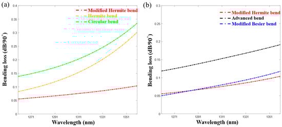
Figure 5.
Simulated bending loss spectra for the TE0 mode at a bending radius of R = 15 µm. (a) Comparison of designs determined via systematic scanning: modified Hermite bend, conventional Hermite bend, and standard circular bend. (b) Comparison of designs optimized via the PSO algorithm: modified Hermite bend, advanced bend [22], and modified Bezier bend [24].
Table 4.
Comparison of simulated insertion losses between the modified Hermite bend and other waveguide bend designs when R = 15 μm.
Mathematically, cubic Hermite and cubic Bezier curves share an identical algebraic basis and are mutually convertible via a linear transformation matrix, as established in geometric modeling theory [29]. Consequently, they possess the same theoretical capacity for describing curve geometries. However, as evidenced in Figure 5b, the modified Hermite bend exhibits superior loss suppression and wavelength stability compared to its Bezier counterpart. This performance discrepancy is not intrinsic to the curves themselves but is attributed to the impact of parameterization efficiency on the heuristic optimization process.
The fundamental distinction lies in the definition of the geometry vector [29]: while the modified Bezier configuration requires four coordinate parameters to implicitly define the boundary derivatives, the modified Hermite formulation exploits the structural symmetry of the 90° bend to explicitly parameterize the tangent vector magnitudes. This reduces the search space dimensionality to merely two adjustable variables (a1, a2). By decoupling the tangent magnitudes from spatial coordinates, this reduction effectively mitigates the parameter redundancy and coupling inherent in the Bezier control polygon. Consequently, this streamlined parameterization minimizes the risk of the PSO algorithm stagnating in local optima and significantly accelerates convergence by lowering the computational overhead of 3D-FDTD iterations.
To evaluate the fabrication tolerance of the modified Hermite bend, we analyzed the influence of waveguide width and height variations of ±20 nm. We used 3D-FDTD simulations to evaluate the modified Hermite bend with a radius of 15 µm under varying width and height conditions. As illustrated in Figure 6a, our proposed design exhibits minimal loss variation across a 100 nm wavelength range under width deviations of ±20 nm. As shown in Figure 6b, it is observed that height has a more pronounced impact on the loss of the bent waveguide compared to width.
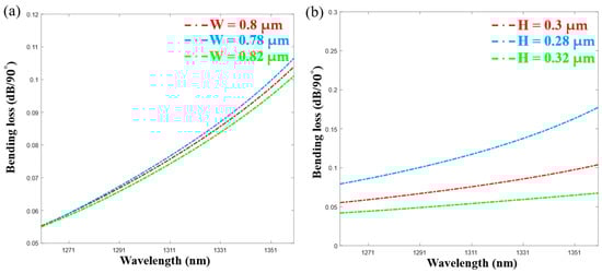
Figure 6.
Simulated bending loss spectra of (a) Width (W) ± 20 nm (b) Height (H) ± 20 nm modified Hermite bends for R = 15 µm.
5. Discussion
The performance of the proposed modified Hermite bent waveguide is evaluated by comparison with state-of-the-art SiN bent waveguides, as summarized in Table 5. Most comparative designs are optimized for the C-band, while the proposed design focuses on the O-band—a critical wavelength range for short-reach data center communications [4]. Meanwhile, this design exhibits superior wavelength insensitivity, as shown in Figure 6a, and adopts a compact cross-section of 800 nm × 300 nm, which is more conducive to high-density integration. The graded-width Hermite curve design enhances the optical field confinement capability, illustrated in Figure 7, shifting the peak of the mode field away from the waveguide sidewalls and reducing scattering loss. Additionally, the design demonstrates robust fabrication tolerance: minimal loss fluctuation is observed under a waveguide width deviation of ±20 nm.
Table 5.
Comparison of Simulated Losses for Different SiN Bent Waveguides.
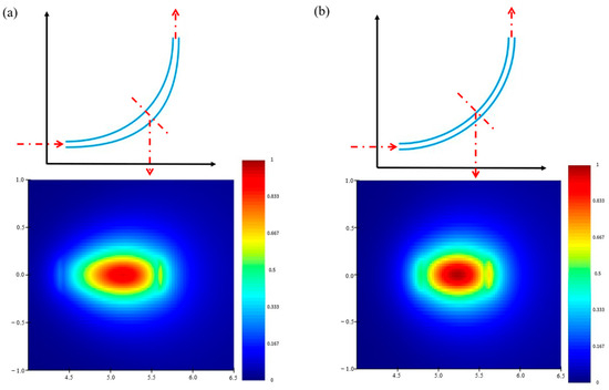
Figure 7.
Simulated cross-sectional mode field intensity distributions at the 45° position for bent waveguides with R = 15 µm at 1311 nm. (a) Conventional circular bent waveguide; (b) Modified Hermite bent waveguide.
6. Conclusions
The proposed methodology facilitates the efficient design of small-radius, low-loss O-band SiN bends using only two parameters, which simultaneously reduces computational overhead. Fundamentally, this approach constitutes an interpolating polynomial, which could be further optimized in future work by configuring additional position coordinates and tangents. This methodology can also be extended to the structural design of a wider range of devices. Its potential for large-scale photonic integration establishes it as a significant contribution to the progress of this field.
In summary, we propose an efficient bent waveguide design methodology that employs a modified Hermite curve and the particle swarm optimization (PSO) algorithm to determine the geometry of the curve. Using this method, we design low-loss O-band SiN bends with radii of 15 µm, 20 µm, 25 µm, and 30 µm. The comparison with other bending design methods shows that the proposed method not only exhibits lower loss but also demonstrates superior wavelength insensitivity and process tolerance.
Author Contributions
Conceptualization, D.L. and L.Z.; methodology, D.L., E.Z., Y.X., L.Z., Y.Z. and X.Y.; software, D.L., E.Z. and X.Y.; validation, D.L., E.Z., Y.X. and Y.Z.; formal analysis, D.L., E.Z., Y.X. and L.Z.; investigation, D.L. and L.Z.; resources, D.L., L.Z. and X.Y.; data curation, D.L., Y.Z.; writing—original draft preparation, D.L.; writing—review and editing, D.L., E.Z., Y.X., L.Z., Y.Z. and X.Y.; visualization, D.L.; supervision, D.L., E.Z., Y.X., L.Z., Y.Z. and X.Y.; project administration, D.L., L.Z. and X.Y.; funding acquisition, L.Z., E.Z. and X.Y. All authors have read and agreed to the published version of the manuscript.
Funding
This work was supported in part by the Fund of State Key Laboratory of Information Photonics and Optical Communications (Beijing University of Posts and Telecommunications) (IPOC2024ZZ03), China, in part by the National Natural Science Foundation of China (U24B20135), in part by the BUPT Excellent Ph.D. Students Foundation (CX20242039), and in part by Beijing Natural Science Foundation (L259017).
Institutional Review Board Statement
Not applicable.
Informed Consent Statement
Not applicable.
Data Availability Statement
The original contributions presented in this study are included in the article. Further inquiries can be directed to the corresponding author.
Conflicts of Interest
The authors declare no conflicts of interest.
References
- Blumenthal, D.J.; Heideman, R.; Geuzebroek, D.; Leinse, A.; Roeloffzen, C. Silicon Nitride in Silicon Photonics. Proc. IEEE 2018, 106, 2209–2231. [Google Scholar] [CrossRef]
- Li, Z.; Fan, Z.; Zhou, J.; Cong, Q.; Zeng, X.; Zhang, Y.; Jia, L. Process Development of Low-Loss LPCVD Silicon Nitride Waveguides on 8-Inch Wafer. Appl. Sci. 2023, 13, 3660. [Google Scholar] [CrossRef]
- Kim, E.; Carpenter, L.; Smith, A.M.; Tison, C.C.; Coleman, D.; Leake, G.; Fanto, M.; Rizzo, A.J.; García-Blanco, S.M.; Cheben, P. Ultra-low loss dispersion-engineered silicon nitride waveguides on 300 mm wafers. In Proceedings of the Integrated Optics: Devices, Materials, and Technologies XXIX, San Francisco, CA, USA, 27–30 January 2025. [Google Scholar] [CrossRef]
- Chandran, S.; Bian, Y.; Lee, W.S.; Abumazwed, A.; Liu, N.; Xu, L.; Ding, H.; Aboketaf, A.; Rakowski, M.; Dezfulian, K.; et al. High performance silicon nitride passive optical components on monolithic silicon photonics platform. In Proceedings of the Optical Fiber Communication Conference, San Diego, CA, USA, 24–28 March 2024. [Google Scholar] [CrossRef]
- Bauters, J.F.; Heck, M.J.R.; John, D.D.; Barton, J.S.; Bruinink, C.M.; Leinse, A.; Heideman, R.G.; Blumenthal, D.J.; Bowers, J.E. Planar waveguides with less than 0.1 dB/m propagation loss fabricated with wafer bonding. Opt. Express 2011, 19, 24090–24101. [Google Scholar] [CrossRef] [PubMed]
- Liu, K.; Jin, N.; Cheng, H.; Chauhan, N.; Puckett, M.W.; Nelson, K.D.; Behunin, R.O.; Rakich, P.T.; Blumenthal, D.J. Ultralow 0.034 dB/m loss wafer-scale integrated photonics realizing 720 million Q and 380 μW threshold Brillouin lasing. Opt. Lett. 2022, 47, 1855–1858. [Google Scholar] [CrossRef] [PubMed]
- Xiang, C.; Jin, W.; Bowers, J.E. Silicon nitride passive and active photonic integrated circuits: Trends and prospects. Photon. Res. 2022, 10, A82–A96. [Google Scholar] [CrossRef]
- Taniguchi, H.; Nakamura, M.; Hamaoka, F.; Mori, T.; Shibahara, K.; Matsui, T. 1.6-Tb/s 10-km transmission in O-band using 400-Gb/s/lane SDM channels enhanced by trellis path-limitation MLSE. J. Light. Technol. 2024, 42, 4338–4346. [Google Scholar] [CrossRef]
- Lu, H.-Y.; Tang, C.-T.; Chen, C.-H.; Tan, B.-X.; Liu, W.-K.; Chiang, H.-Y. Low-loss high-uniformity silicon nitride optical building blocks integrated on silicon photonics platform. In Proceedings of the 2025 Optical Fiber Communications Conference and Exhibition (OFC), San Francisco, CA, USA, 30 March–3 April 2025; Available online: https://ieeexplore.ieee.org/stamp/stamp.jsp?tp=&arnumber=11046774&isnumber=11046206 (accessed on 8 February 2026).
- Yuan, Y.; Peng, Y.; Sorin, W.V.; Cheung, S.; Huang, Z.; Liang, D.; Fiorentino, M.; Beausoleil, R.G. A 5 × 200 gbps microring modulator silicon chip empowered by two-segment z-shape junctions. Nat. Commun. 2024, 15, 918. [Google Scholar] [CrossRef]
- Ji, X.; Wang, R.N.; Liu, Y.; Riemensberger, J.; Qiu, Z.; Kippenberg, T.J. Efficient mass manufacturing of high-density, ultra-low-loss Si3N4 photonic integrated circuits. Optica 2024, 11, 1397–1407. [Google Scholar] [CrossRef]
- Bose, D.; Harrington, M.W.; Ilicshenko, A.; Liu, K.; Wang, J.; Chauhan, N.; Newman, Z.L.; Blumenthal, D.J. Anneal-free ultra-low loss silicon nitride integrated photonics. Light Sci. Appl. 2024, 13, 156. [Google Scholar] [CrossRef]
- Yang, C.; Pham, J. Characteristic Study of Silicon Nitride Films Deposited by LPCVD and PECVD. Silicon 2018, 10, 2561–2567. [Google Scholar] [CrossRef]
- Rickman, A.G.; Reed, G.T.; Namavar, F. Silicon-on-insulator optical rib waveguide loss and mode characteristics. J. Light. Technol. 1994, 12, 1771–1776. [Google Scholar] [CrossRef]
- Melloni, A.; Carniel, F.; Costa, R.; Martinelli, M. Determination of bend mode characteristics in dielectric waveguides. J. Light. Technol. 2001, 19, 571–577. [Google Scholar] [CrossRef]
- Gao, F.; Qin, L.; Chen, Y.-Y.; Jia, P.; Chen, C.; Liang, L.; Chen, H.; Zhang, X.; Ning, Y.-Q. Research progress of bent waveguide and its applications. Chin. Opt. 2017, 10, 176–193. [Google Scholar] [CrossRef]
- Collin, R.E. Field Theory of Guided Waves, 2nd ed.; Wiley-IEEE Press: New York, NY, USA, 1991; pp. 1–864. Available online: https://ieeexplore.ieee.org/book/5265444 (accessed on 8 February 2026).
- Kitoh, T.; Takato, N.; Yasu, M.; Kawachi, M. Bending loss reduction in silica-based waveguides by using lateral offsets. J. Light. Technol. 1995, 13, 555–562. [Google Scholar] [CrossRef]
- Song, J.H.; Kongnyuy, T.D.; Stassen, A.; Mukund, V.; Rottenberg, X. Adiabatically bent waveguides on silicon nitride photonics for compact and dense footprints. IEEE Photonics Technol. Lett. 2016, 28, 2164–2167. [Google Scholar] [CrossRef]
- Vogelbacher, F.; Nevlacsil, S.; Sagmeister, M.; Kraft, J.; Unterrainer, K.; Hainberger, R. Analysis of silicon nitride partial Euler waveguide bends. Opt. Express 2019, 27, 31394–31406. [Google Scholar] [CrossRef]
- Song, J.H.; Kongnyuy, T.D.; De Heyn, P.; Lardenois, S.; Jansen, R.; Rottenberg, X. Low-loss waveguide bends by advanced shape for photonic integrated circuits. J. Light. Technol. 2020, 38, 3273–3279. [Google Scholar] [CrossRef]
- Song, J.H.; Kongnyuy, T.D.; Prost, M.; Bandyopadhyay, A.; Dwivedi, S.; Carbajal Altamirano, D. Advanced bends and micro ring resonators in silicon nitride photonic waveguides for C-band. IEEE Photonics J. 2024, 16, 1–5. [Google Scholar] [CrossRef]
- Gao, F.; Xie, W.; Li, B.; Bu, X.; Song, A.; Luo, X. Low-loss and compact bends on multi-layer SiN-on-SOI platform for photonic integrated circuits. IEEE Photonics Technol. Lett. 2021, 33, 1131–1134. [Google Scholar] [CrossRef]
- Sun, T.; Xia, M. Low loss modified Bezier bend waveguide. Opt. Express 2022, 30, 10293–10305. [Google Scholar] [CrossRef]
- Pita Ruiz, J.L.; Dalvand, N.; Ménard, M. Inverse-designed 90-degree silicon nitride bends for the C band. J. Light. Technol. 2025, 43, 5804–5810. [Google Scholar] [CrossRef]
- Chen, X.; Li, Q.; Zheng, K.; Li, Y. Research and application of obstacle avoidance path planning based on Hermite curve interpolation. In Proceedings of the 2023 5th International Conference on Robotics, Intelligent Control and Artificial Intelligence (RICAI), Hangzhou, China, 1–3 December 2023. [Google Scholar] [CrossRef]
- Zhang, L.; Wang, K.; Chen, J.; Ma, T.; Li, W.; An, J. Ultra-compact low-loss modified N-adjustable bends. J. Light. Technol. 2023, 41, 2792–2800. [Google Scholar] [CrossRef]
- Tao, P.; Yan, B.; Bai, M.; Zhou, M.; Sun, C.; Qi, Y.; Wang, Y.; Han, Z.; Fan, Y.; Wang, Q. Ultrahigh Q SOI ring resonator with a Hermite or B-spline curved waveguide. Appl. Opt. 2024, 63, 6233–6239. [Google Scholar] [CrossRef]
- Hughes, J.F.; van Dam, A.; McGuire, M.; Sklar, D.F.; Foley, J.D.; Feiner, S.K.; Akeley, K. Splines and Subdivision Curves. In Computer Graphics: Principles and Practice, 3rd rev. ed.; Hughes, J.F., van Dam, A., McGuire, M., Sklar, D.F., Foley, J.D., Feiner, S.K., Akeley, K., Eds.; Addison-Wesley: Reading, MA, USA, 2014; pp. 595–598. [Google Scholar]
- Chamorro-Posada, P. Silicon Nitride Bent Asymmetric Coupled Waveguides with Partial Euler Bends. Photonics 2024, 13, 218. [Google Scholar] [CrossRef]


Disclaimer/Publisher’s Note: The statements, opinions and data contained in all publications are solely those of the individual author(s) and contributor(s) and not of MDPI and/or the editor(s). MDPI and/or the editor(s) disclaim responsibility for any injury to people or property resulting from any ideas, methods, instructions or products referred to in the content. |
© 2026 by the authors. Licensee MDPI, Basel, Switzerland. This article is an open access article distributed under the terms and conditions of the Creative Commons Attribution (CC BY) license.