Abstract
A scheme of a photonic convolution processor based on a tunable electro-optic frequency comb is proposed. The optical frequency comb (OFC) is generated using a dual-parallel Mach–Zehnder modulator (DPMZM) driven by an RF signal. By adjusting the working parameters of the DPMZM, OFCs with different line number and frequency spacing can be produced to reconfigure the convolution kernel dimensions. A linearly chirped fiber Bragg grating (LCFBG) is employed to implement interleaving of temporal and spectral dimensions. The interleaved signals are sampled at specific time and summed after optoelectronic conversion, and the convolution operation is completed. In this work, using a 10 GHz RF signal, a 4-line OFC with a frequency spacing of 20 GHz and a 2-line OFC with a spacing of 40 GHz are generated to obtain a 2 × 2 and 1 × 2 convolution kernels, respectively. The convolution results are fed into an electronic pooling layer and a fully connected layer for classifying the images of the MNIST handwritten digit dataset. The results demonstrate that a classification accuracy of 95.7% is achieved using the 2 × 2 convolution kernel, and a higher classification accuracy of 96.5% is obtained with the 1 × 2 convolution kernel.
1. Introduction
With the rapid development of artificial neural networks (ANNs), convolutional neural networks (CNNs), as an important branch, have been widely applied in fields of image recognition [1], object classification [2] and signal processing [3] due to their exceptional feature extraction capabilities. However, as task complexity increases and neural network model scales expands, electronic neural networks based on the traditional von Neumann architecture are facing growing challenges in computational speed, energy efficiency, and hardware scalability [4]. To overcome these limitations, photonic neural networks have been proposed. In such networks, lightwaves are employed as information carriers, and functionalities of neural networks are realized through photonic devices, characterized by high-speed operation, large bandwidth, strong parallelism, and low power consumption [5].
In photonic neural networks, photonic convolution has become a research focus. It can be implemented employing spatial optical devices such as a diffractive optical element or a spatial light modulator. And high-speed convolution has been experimentally demonstrated by use of these devices [6,7]. However, this approach suffers from relatively large system volumes. To overcome this limitation, a photonic convolution method based on integrated optical devices has been proposed. In [8], the photonic convolution was carried out via vector matrix multiplication realized by properly combining multiple 2 × 2 thermally tunable Mach–Zehnder interferometers (MZIs). According to the Singular Value Decomposition theorem, this scheme can be extended to achieve vector matrix multiplications with an arbitrary 4 × 4 MZI mesh. Similarly, an integrated diffractive neural network (IDNN) was proposed in [9], and it comprised ten MZIs and two diffractive units. As a basic computing unit, a MZI consisted of multimode interferometers-based beam splitters and two thermo-optic phase shifters. The two diffractive units were composed of a slab waveguide to perform Fourier transform and inverse Fourier transform, respectively. The functionality of this IDNN was experimentally validated on MNIST and Fashion-MNIST datasets, and the classification accuracy was, respectively, 91.4% and 80.4%. Another programmable integrated photonics platform was also designed in [10], and it consisted of a hexagonal mesh of silicon-based MZIs whose transfer matrix can be programmed by adjusting the embedded thermo-optic phase shifters. This enables a nearly universal platform for the implementation of linear optical operations by interfering signals from different paths. However, the cascading of multiple MZIs resulted in a relatively high power loss.
Photonic convolution can also be realized using wavelength-division multiplexing (WDM) technology, which is characterized by the interleaving of temporal, spectral and spatial dimensions. In this method, convolution kernels are generated by shaping a spectrum of a multi-wavelength source, i.e., an optical frequency comb (OFC). And multiple parallel convolution links are spatially established using dispersive components, ensuring modulated signals interleaved in both time and wavelength, thereby enabling convolution operations. The commonly used optical sources include micro-ring resonators (MRRs), mode-locked lasers (MLLs) and integrated multi-wavelength laser arrays (MLAs). In [11], an OFC from an MRR was shaped to generate convolution kernels. A computational speed of 11.3 trillions of operation per second (TOPS) was achieved, enabling convolution on large-scale images of 250 k pixels. Similarly, an MLL was employed to construct a photonics-enabled CNN in [12], where large-scale matrix operations for two kernels were realized simultaneously. On the MNIST handwritten digit dataset, an accuracy of 90.04% was obtained. The application of scalable MLAs in photonic CNNs was investigated in [13]. It was experimentally demonstrated that even with a 25% deviation in wavelength spacing, a recognition accuracy of 91.2% on the MNIST handwritten digit dataset was maintained, highlighting an excellent fault tolerance. In these works, dispersion delay was introduced by a section of single-mode fiber (SMF) [11,13] or dispersion compensation fiber (DCF) [12] to achieve interleaving in time and wavelength, which inevitably resulted in a larger system volume and a higher power loss. In another microwave photonic convolution processor proposed in [14], a linearly chirped fiber Bragg grating (LCFBG) was used as a dispersion component. In [15], an integrated microcomb-driven photonic processing unit was implemented, and Si spiral waveguides are embedded to introduce on-chip time delays. Compared to the previously mentioned implementations, the WDM-based optical convolution makes full use of abundant spectral resources, supports the construction of large-scale neural networks, and significantly enhances the computational efficiency and applicability of photonic neural networks.
It is known that an OFC can also be generated via electro-optic modulation, and this method has the advantages of high tunability and stability [16,17]. As far as we know, electro-optic frequency combs have not been applied in photonic convolution. In this work, a scheme of photonic convolution processor is proposed by using a tunable electro-optic frequency comb generator based on a dual-parallel Mach–Zehnder modulator (DPMZM). Also, to increase the system integration and reduce the loss, a LCFBG is employed to provide dispersion delay. The DPMZM is driven by a 10 GHz RF signal. A 4-line OFC with a frequency spacing of 20 GHz and a 2-line OFC with a spacing of 40 GHz are, respectively, generated by adjusting the working parameters of this DPMZM. In this way, a 2 × 2 and a 1 × 2 convolution kernels are, respectively, obtained and applied in the task of handwritten digit recognition. The classification accuracy is 95.7% and 96.5% when the two convolution kernels are, respectively, used. So this photonic convolution scheme based on a tunable electro-optic frequency comb can achieve different classification accuracy for different applications.
2. Principles
A schematic diagram of the photonic convolutional computation is shown in Figure 1a. The lightwave from a continuous wave (CW) laser is modulated via a DPMZM, and an RF signal is divided into two parts with a phase difference to drive the two sub-MZMs of this DPMZM. Consequently, an OFC is generated, and they are used as a 1 × N2 weight vector W corresponding to an N × N convolution kernel weight matrix, as shown in Figure 1b. Each element Wi is assigned to a comb line of the OFC with a wavelength of λi and its value is mapped to the intensity of this line. The input image is flattened into a one-dimensional vector X, which is encoded by an arbitrary waveform generator (AWG) into an electrical signal at a specific symbol rate. This signal drives an intensity modulator (IM) to modulate the OFC generated by the DPMZM. After modulation, the output signal representing the product of X and W is injected into a LCFBG through an optical circulator, where different time delays are introduced to different wavelengths. The delay difference between adjacent spectral lines corresponds to the duration of one pixel in the image. The delayed optical signal is demultiplexed and for each wavelength channel optoelectronic conversion is realized via a photo-detector (PD). Finally, the product results from all wavelength channels are summed, and the final convolution result Yi is obtained by extracting signals at specific time as shown in Figure 1b.
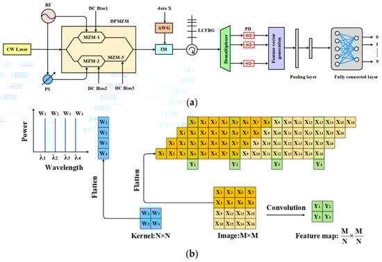
Figure 1.
(a) Schematic diagram of the photonic convolution processor based on a tunable electro-optic frequency comb. (CW Laser: continuous wave laser; RF: Radio frequency; PS: Phase shifter; DPMZM: Dual-parallel Mach–Zehnder modulator; AWG: Arbitrary waveform generator; IM: Intensity modulator; LCFBG: Linearly chirped fiber Bragg grating; PD: Photo-detector). (b) Principle of photonic convolution including the process of flattening the convolution kernel and input data.
The DPMZM employed in the system is composed of two sub-modulators, MZM-1 and MZM-2, as well as a main modulator MZM-3. The signal from the RF source is divided equally into two branches to drive the two sub-modulators. The output field of the DPMZM can be written as follows [18]:
where Ein(t) = E0exp[jω0t + ϕlaser(t)] and Eout(t) are, respectively, the input and output optical field. E0 and ω0 are, respectively, the amplitude and the angular frequency of the CW laser, and ϕlaser(t) is the phase noise induced by the linewidth of the laser, Δνlaser. For a time interval τ, the variation in this phase noise Δϕlaser(τ) = ϕlaser(t + τ) − ϕo(t) is with a normal distribution N(0, 2πΔνlaser|τ|) according to Floquet theory [19]. s1(t) = m1Vπ1cos(ωmt) and s2(t) = m2Vπ2cos(ωmt + θ) are the RF signals driving MZM-1 and MZM-2. m1 = Vm1/Vπ1 and m2 = Vm2/Vπ2 are the modulation depth of the two sub-MZMs. Vm1 and Vm2 are the amplitudes of the driving signals, ωm is the frequency of the RF signal, and θ is the phase difference between the two RF signals, which is adjusted by a phase shifter (PS). Vπ1 and Vπ2 are the half-wave voltages of MZM-1 and MZM-2. ϕ1, ϕ2, and ϕ3 are, respectively, the fixed phase shifts introduced by the DC bias voltages applied to MZM-1, MZM-2, and MZM-3. Different OFCs can be generated by adjusting these working parameters.
The LCFBG in Figure 1a is designed by modulating the refractive index of the fiber core using an apodization function, and a stop band is formed in the frequency domain, causing the incident light to be reflected [20]. For a linearly chirped fiber grating, the grating pitch or grating period variation Φ(z) is
where F represents the chirp rate and L is the grating length.
The used apodization function is the Tanh function, expressed as
where δneff denotes the variation in the average refractive index, α = 3 and β = 4. By adjusting the length and chirp rate of the LCFBG, the induced delay difference between signals at different wavelength can correspond to the duration of one pixel in an image.
After the time delay, the signal at each wavelength is demultiplexed and converted into an electrical signal by a PD. As shown in Figure 1b, by sampling this signal at each channel at a specific time, the convolution operation for feature extraction is completed after summing up the sampled signals. The generated feature vectors are then fed into a pooling layer and a fully connected layer, as seen from Figure 1a. Nonlinearity is introduced through the ReLU function. Feature compression is carried out by the pooling layer to reduce the dimensionality of the feature vectors. Finally, based on the output from the fully connected layer, the classification results are obtained.
3. Results
The MNIST handwritten digit dataset is employed in the experiment. Each 28 × 28 pixel grayscale image is flattened into a one-dimensional vector X. In the simulation, the data rate is 10 Gigabaud with a duration of 100 ps per pixel. The central wavelength of the CW Laser with a linewidth of 50 kHz is 1550 nm and the output power is 10 mW. An optical frequency comb is generated using a DPMZM, with each spectral line corresponding to a weight position in the convolution kernel. The frequency of the RF signal driving the DPMZM is 10 GHz. A 2 × 2 and a 1 × 2 convolution kernel are, respectively, employed for feature extraction.
For the case of a 2 × 2 convolution kernel used, the main modulator of the DPMZM is biased at the ground, while the two sub-modulators are both biased at the minimum transmission points to generate a 4-line OFC with a spacing of 20 GHz, i.e., 0.16 nm. The phase difference between the two driving signals applied to MZM-1 and MZM-2 is set to 0. In this case, Equation (1) can be simplified, and the output field of the DPMZM can be written as
where Jn(x) represents the n-th order Bessel function of the first kind. In order to generate a 2 × 2 convolution kernel [1 1 1 1], the 4-line OFC is expected to be with a flatness and a sideband suppression ratio (SBSR) as high as possible. Here, the flatness is defined as the power difference in the 4 spectral lines, and the SBSR is the ratio between the minimal intensity of the 4 lines to the maximum intensity of the other lines in the spectrum output from the DPMZM. So, the modulation depths m1 and m2 of the two sub-modulators need to be optimized. Two contour plots as a function of m1 and m2 are shown in Figure 2a,b, where the z-axial is, respectively, the flatness and the SBSR of the OFC. To generate a comb with a flatness below 1 dB and a SBSR higher than 15 dB, m1 and m2 are set to be 0.96, denoted as point A in the two contour plots.
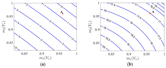
Figure 2.
Contour plots as a function of m1 and m2, and the z-axial is the flatness (a) and the sideband suppression ratio (b) of the OFC output from the DPMZM, and m1 = m2 = 0.96 corresponding to point A is used to generate a comb with a flatness below 1 dB and a SBSR higher than 15 dB.
With the working parameters determined above, the output spectrum of the DPMZM is presented in Figure 3a. As expected, the line spacing is 0.16 nm, and the four center lines has a flatness of 0.6 dB and a SBSR of 17 dB without any other spectral shaping. This OFC is then modulated by the electrical signal encoded from the handwritten digit image vector via an IM, as shown in Figure 1a. The output spectrum of the IM is shown in Figure 3b. Comparing the two figures, it can be found that the OFC lines are modulated with more frequency components observed beside them.
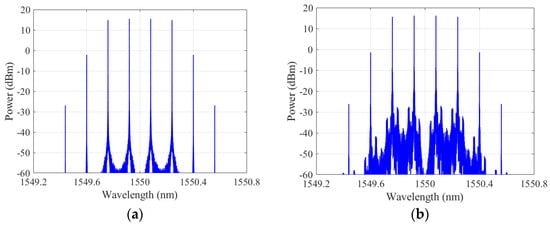
Figure 3.
The spectra at the output of the DPMZM (a) and the IM (b) in the case of a 2 × 2 convolution kernel used.
The modulated OFC is then sent to the LCFBG, which introduces different time delays to signals at different wavelengths. To achieve a time shift between two adjacent wavelengths equal to the duration of one pixel, which is 100 ps, the LCFBG is designed with a length of L = 6.2 cm, a chirp rate of F = 142π, and the value of δneff in the apodization function is 1.2 × 10⁻⁴. The reflection spectrum and time delay characteristics of the grating are given in Figure 4. Within the wavelength range from 1549.76 nm to 1550.24 nm, the reflectivity is nearly equal. The slope of the time delay curve corresponds to the dispersion parameter D of the LCFBG, and it is 637.3 ps/nm after linear fitting. So, a delay difference of 101.97 ps is achieved per 0.16 nm wavelength interval, corresponding to a 100 ps duration of per pixel.
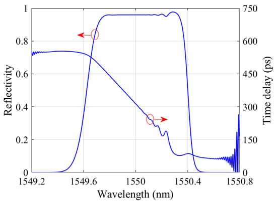
Figure 4.
The reflection spectrum and time delay characteristics of the used LCFBG. The circle and arrow are combined to indicate the curves respectively corresponding to the left and the right y-axis.
After the time delay and demultiplexing, the signal at each wavelength is converted into an electrical signal by the PD. The converted signals from the four channels are collected and processed, and the final convolution result is obtained by sum of the four signals at specific positions. In this way, feature vectors are generated, as shown in Figure 1a. In our study, up to 5000 images from the MNIST dataset are selected for training, and another 1000 images are for testing. All images are first processed by the photonic convolution processor, where the resulting feature vectors are used to generate corresponding feature images. Taking the digits “3”, “6”, and “8” as examples, the original images and their generated feature images are, respectively, shown in Figure 5a,b.
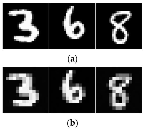
Figure 5.
The original images from the MNIST handwritten digit dataset (a) and the generated feature images using a 2 × 2 kernel (b).
The obtained feature vectors are then fed to a pooling layer and an electronic fully connected layer. Classification results are output after the nonlinear activation function of Softmax. The classification accuracy of testing 1000 images is 95.7%, and the confusion matrix is presented in Figure 6, where a detailed classification performance across different categories is revealed. It can be found that misclassification rates are relatively higher when recognizing the digits of “2”, “5”, and “8”.
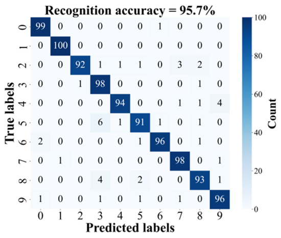
Figure 6.
The confusion matrix with a 2 × 2 convolution kernel used.
When a 1 × 2 convolution kernel [1 1] is employed, an OFC with a line spacing of 0.32 nm is required to achieve feature extraction with the convolution processor in Figure 1a. To generate such a 2-line OFC, MZM-1 and MZM-2 are also biased at the minimum transmission points, and the phase shift introduced by the DC bias of MZM-3 is ϕ3 = π/2. The phase difference between the RF signals driving the two sub-modulators is set to π/2. In this case, the output field of the DPMZM can be written as
From Equation (5), it can be found that with m1 = m2 = m, the 3rd and −1st sidebands are suppressed, and the remaining −3rd and 1st sidebands form a dual-tone OFC with a line spacing of 40 GHz. Figure 7 shows the flatness and the SBSR of this OFC as a function of the modulation depth m. In the same way as the above case, to generate a comb with a flatness below 1 dB and a SBSR higher than 15 dB, the modulation depths of both sub-modulators are set to 0.96.
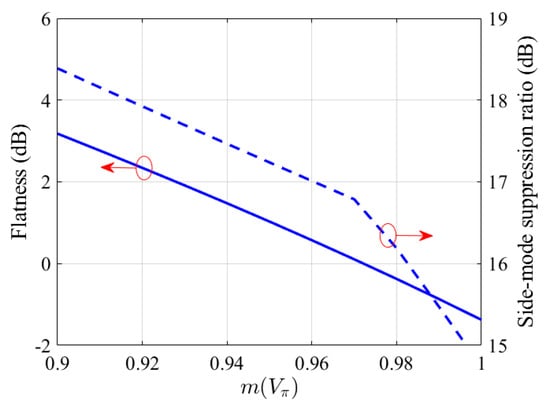
Figure 7.
The flatness and the SBSR of the generated 2-line OFC as a function of the modulation depth, m. The circle and arrow are combined to indicate the curves corresponding to the left and the right y-axis.
In this case, the output spectrum of the DPMZM is shown in Figure 8a. Also, as expected, the line spacing is 0.32 nm, and the flatness and SBSR are, respectively, 0.6 dB and 17 dB. After this, the OFC is modulated by the electrical signal encoded from the handwritten digit image vector, and the output spectrum of the IM is presented in Figure 8b. It can be observed that the modulation of the two comb lines is also achieved.
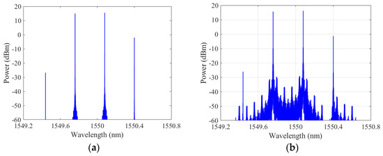
Figure 8.
The spectra at the output of the DPMZM (a) and the IM (b) for the case of a 1 × 2 convolution kernel employed.
The modulated OFC is then sent to the LCFBG to implement the interleaving of temporal and spectral dimensions. After reflection in the grating, the signal is demultiplexed and photo-electrically converted by PDs. The output signals from the two wavelength channels are sampled at a specific time and summed to obtain the final convolution results. For this case of a 1 × 2 convolution kernel used, the sampling method is shown in Figure 9. It can be found that the delay difference between the two comb lines is two pixel-durations, and this can be realized by the above used LCFBG since the line spacing is doubled.
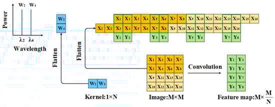
Figure 9.
Principle of photonic convolution including the process of flattening the convolution kernel and input data with a 1 × 2 convolution kernel used.
Using the same training and testing sets from the MNIST dataset as those in the case of a 2 × 2 convolution kernel employed, the resulting feature vectors are obtained by the photonic convolution processor. And the corresponding feature images are shown in Figure 10a, also taking the digits “3”, “6”, and “8” as examples. After training, classification results on the testing set are collected. The results demonstrate that a higher classification accuracy of 96.5% is achieved. The confusion matrix presented in Figure 10b also provides a detailed classification performance across different categories, revealing that the misclassification rate is relatively higher for digits “3”, “4”, and “5”.
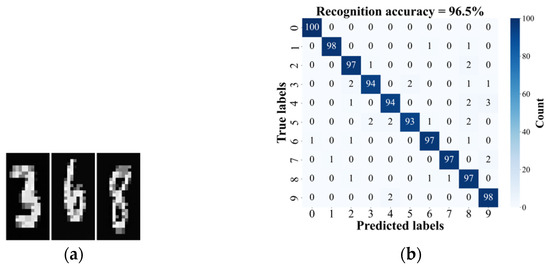
Figure 10.
The generated feature images (a) and the confusion matrix (b) with a 1 × 2 convolution kernel used.
4. Discussion
From the above results, it is clear that a classification accuracy of 95.7% is realized by the optoelectronic hybrid neural network constructed in this work employing a 2 × 2 convolutional kernel. The effective convolution speed is calculated as the ratio of useful columns to total columns [14]. It is 0.25 × fs, fs, which is the modulation speed for a comb line, where fs = 10 GHz. A higher classification accuracy of 96.5% is achieved by the system using a 1 × 2 convolutional kernel, with an effective convolution speed of 0.5 × fs. To further quantify the performance differences between our work and the other photonic convolution methods based on WDM technology, the proposed method using the electro-optic frequency comb is compared with those of representative photonic convolution processors based on MRR, MLLs, and MLAs in Table 1. It can be seen that the computational throughput of our method is lower than the other approaches, mainly due to only one convolution kernel being employed. However, a 95–96% classification accuracy on the MNIST dataset is achieved with our method. In [15], a higher accuracy was achieved by use of three 2 × 2 convolution kernels, and three feature maps were generated, resulting in an increased complexity in fully connected layers. So, we can safely believe that our method has a competitive performance compared with the existing methods. Furthermore, our method offers a significantly enhanced flexibility. By adjusting the working parameters of the DPMZM, OFCs with different line numbers and frequency spacing can be generated. This enables reconfiguration of the convolution kernel dimensions to meet accuracy requirements in different applications. In the following, more discussions on the practical implementation and future development of the system are presented.

Table 1.
Comparison of the proposed approach and the other WDM-based methods.
4.1. Scalability
To further extend the dimensions of the convolution kernel, the number of comb lines can be increased by adjusting the modulation depth of the two sub-MZMs. For example, when the main modulator of the DPMZM is biased at the ground, and the two sub-modulators are both biased at the minimum transmission points, a 6-line OFC can also be generated with a spacing of 0.16 nm. In the same way for a 4-line OFC generation, the modulation depths of the two sub-modulators (m1 and m2) are optimized, and they are, respectively, set to 1.85 and 1.45 to obtain a flatness < 1 dB, denoted as point B in Figure 11a. The resulting output spectrum of the DPMZM is given in Figure 11b. As expected, the line spacing is 0.16 nm, and the flatness is 0.55 dB. This 6-line OFC enables the implementation of a 2 × 3 convolution kernel and supports dynamic reconfiguration of the kernel dimensions. However, for the applications of deeper photonic neural networks, a DPMZM with a lower half-wave voltage and a higher maximum allowable driving power is required. At the same time, as the system bandwidth is widened with the number of comb lines increasing, the length and chirp rate of the LCFBG need to be adjusted to achieve a linear dispersion response over a broader bandwidth.
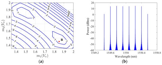
Figure 11.
Contour plot as a function of m1 and m2 (a), and the corresponding spectrum output from the DPMZM (b). In (a), the z-axial is the flatness of the OFC, m1 = 1.85 and m2 = 1.45 corresponding to point B are used to generate a comb with a flatness < 1 dB.
4.2. Considerations in Experiments
In practical experiments, some other issues still need to be taken into account. Firstly, a high-precision bias voltage control circuit is required to effectively avoid the drift of the DPMZM bias points. Secondly, to compensate the insertion loss of the LCFBG, an erbium-doped fiber amplifier is also needed, while the dispersion ripple in LCFBG can be suppressed by use of a temperature control. In addition, PDs with a wider bandwidth and low noise are indispensable.
It should be noted that the system’s accuracy is also affected by the phase noise of the used CW laser. The accuracy in the cases of different laser linewidths is shown in Figure 12 when a 2 × 2 and a 1 × 2 convolution kernels are, respectively, used. It is clear that the linewidth increases as the phase noise grows, leading to a decrease in accuracy. Under the same laser linewidth condition, using a 1 × 2 convolution kernel can obtain a higher accuracy. So, a CW laser with a linewidth as narrow as possible is also required in a deeper photonic neural network with a large-sized convolution kernel used.
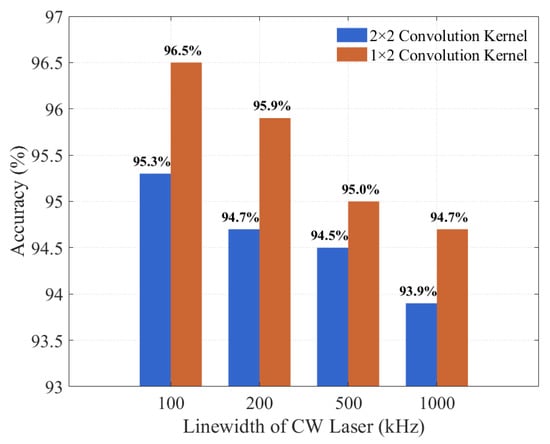
Figure 12.
Comparison of system accuracy in the cases of different CW laser linewidths with a 2 × 2 and a 1 × 2 convolution kernels, respectively, used.
4.3. Prospects
With the continuous advancements in micro–nano fabrication technology, an increasing number of optoelectronic components can be integrated on an optical platform. Integrated optoelectronic oscillators (OEOs) have been demonstrated with an excellent performance of low phase noise and high spectral purity [21]. So, it can be believed that a traditional RF source will be replaced by an OEO, and an integrated self-oscillating electro-optic frequency comb can be achieved in near future. On the other hand, programmable photonic circuits have been frequently proposed for realizing linear transformations; e.g., a quantum frequency processor and a LiNbO3-based photonic fast Fourier transform processor were, respectively, demonstrated as a three-dimensional frequency beam-splitter [22] and an onboard data processor in an all-optical synthetic aperture radar [23]. Recently, by leveraging the dispersion of coupled waveguide arrays, a four-port programmable silicon photonic circuit was designed for linear space–frequency transformations in [24]. All these achievements enable that the interleaving of temporal, spectral, and spatial dimensions can be realized within a compact on-chip photonic circuit. So, an OEO-based OFC generator combined with a programmable photonic circuit will also push the field of WDM-based photonic convolution processors forward.
5. Conclusions
A photonic convolution processor based on a tunable electro-optic frequency comb is designed and applied in the classification task on the MNIST dataset. A 4-line OFC with a frequency spacing of 20 GHz and a 2-line OFC with a spacing of 40 GHz are, respectively, generated by adjusting the working parameters of a DPMZM, enabling a flexible reconfiguration of convolution kernels. The interleaving of temporal and spectral dimensions are realized through a LCFBG, and the convolution operation is completed after extraction at specific time to obtain feature vectors of the input images. The simulation results demonstrate that a classification accuracy of 95.7% is achieved with the 2 × 2 convolution kernel, while a higher accuracy of 96.5% is attained using the 1 × 2 convolution kernel. So, this tunable electro-optic frequency comb-based photonic convolution processor has the advantage of significantly enhanced flexibility, and it can be applied in a future photonic neural network to meet different accuracy requirements.
Author Contributions
Conceptualization, J.Y.; methodology, J.Y. and J.W.; software, J.W.; validation J.Y.; formal analysis, J.Y. and J.W.; investigation, J.W.; resources, J.W.; data curation, J.W.; writing—original draft preparation, J.W.; writing—review and editing, J.Y.; visualization, J.W.; supervision, J.Y.; project administration, J.Y.; funding acquisition, J.Y. All authors have read and agreed to the published version of the manuscript.
Funding
This research was supported by the National Natural Science Foundation of China (NSFC) (61771029, 61201155).
Data Availability Statement
Data underlying the results presented in this paper are not publicly available but may be obtained from the authors upon reasonable request.
Conflicts of Interest
The authors declare no conflicts of interest.
References
- Tian, Y. Artificial Intelligence Image Recognition Method Based on Convolutional Neural Network Algorithm. IEEE Access 2020, 8, 125731–125744. [Google Scholar] [CrossRef]
- Huang, J.; Huang, S.; Zeng, Y.; Chen, H.; Chang, S.; Zhang, Y. Hierarchical Digital Modulation Classification Using Cascaded Convolutional Neural Network. J. Commun. Inf. Netw. 2021, 6, 72–81. [Google Scholar] [CrossRef]
- Yang, X.; Zhu, Z.; Jiang, G.; Wu, D.; He, A.; Wang, J. DC-ASTGCN: EEG Emotion Recognition Based on Fusion Deep Convolutional and Adaptive Spatio-Temporal Graph Convolutional Networks. IEEE J. Biomed. Health Inform. 2025, 29, 2471–2483. [Google Scholar] [CrossRef]
- Ambrogio, S.; Narayanan, P.; Tsai, H.; Shelby, R.M.; Boybat, I.; Di Nolfo, C.; Sidler, S.; Giordano, M.; Bodini, M.; Farinha, N.C.P.; et al. Equivalent-Accuracy Accelerated Neural-Network Training Using Analogue Memory. Nature 2018, 558, 60–67. [Google Scholar] [CrossRef] [PubMed]
- Jiang, Y.; Zhang, W.; Yang, F.; He, Z. Photonic Convolution Neural Network Based on Interleaved Time-Wavelength Modulation. J. Light. Technol. 2021, 39, 4592–4600. [Google Scholar] [CrossRef]
- Chang, J.; Sitzmann, V.; Dun, X.; Heidrich, W.; Wetzstein, G. Hybrid Optical-Electronic Convolutional Neural Networks with Optimized Diffractive Optics for Image Classification. Sci. Rep. 2018, 8, 12324. [Google Scholar] [CrossRef] [PubMed]
- Gu, Z.; Gao, Y.; Liu, X. Optronic Convolutional Neural Networks of Multi-Layers with Different Functions Executed in Optics for Image Classification. Opt. Express 2021, 29, 5877. [Google Scholar] [CrossRef]
- De Marinis, L.; Cococcioni, M.; Liboiron-Ladouceur, O.; Contestabile, G.; Castoldi, P.; Andriolli, N. Photonic Integrated Reconfigurable Linear Processors as Neural Network Accelerators. Appl. Sci. 2021, 11, 6232. [Google Scholar] [CrossRef]
- Zhu, H.H.; Zou, J.; Zhang, H.; Shi, Y.Z.; Luo, S.B.; Wang, N.; Cai, H.; Wan, L.X.; Wang, B.; Jiang, X.D.; et al. Space-Efficient Optical Computing with an Integrated Chip Diffractive Neural Network. Nat. Commun. 2022, 13, 1044. [Google Scholar] [CrossRef]
- On, M.B.; Ashtiani, F.; Sanchez-Jacome, D.; Perez-Lopez, D.; Yoo, S.J.B.; Blanco-Redondo, A. Programmable Integrated Photonics for Topological Hamiltonians. Nat. Commun. 2024, 15, 629. [Google Scholar] [CrossRef]
- Xu, X.; Tan, M.; Corcoran, B.; Wu, J.; Boes, A.; Nguyen, T.G.; Chu, S.T.; Little, B.E.; Hicks, D.G.; Morandotti, R.; et al. 11 TOPS Photonic Convolutional Accelerator for Optical Neural Networks. Nature 2021, 589, 44–51. [Google Scholar] [CrossRef]
- Meng, X.; Shi, N.; Shi, D.; Li, W.; Li, M. Photonics-Enabled Spiking Timing-Dependent Convolutional Neural Network for Real-Time Image Classification. Opt. Express 2022, 30, 16217. [Google Scholar] [CrossRef]
- Tang, K.; Ji, X.; Liu, J.; Wang, J.; Xin, Y.; Liu, J.; Wu, G.; Sun, Q.; Zeng, Z.; Xiao, R.; et al. Photonic Convolutional Neural Network with Robustness against Wavelength Deviations. Opt. Express 2023, 31, 37348. [Google Scholar] [CrossRef]
- Chegini, M.; Guan, Y.; Yao, J. A High-Speed Microwave Photonic Processor for Convolutional Neural Networks. In Proceedings of the 2024 International Topical Meeting on Microwave Photonics (MWP), Pisa, Italy, 17–20 September 2024; IEEE: Pisa, Italy, 2024; pp. 1–4. [Google Scholar]
- Bai, B.; Yang, Q.; Shu, H.; Chang, L.; Yang, F.; Shen, B.; Tao, Z.; Wang, J.; Xu, S.; Xie, W.; et al. Microcomb-Based Integrated Photonic Processing Unit. Nat. Commun. 2023, 14, 66. [Google Scholar] [CrossRef]
- Metcalf, A.J.; Torres-Company, V.; Leaird, D.E.; Weiner, A.M. High-Power Broadly Tunable Electrooptic Frequency Comb Generator. IEEE J. Sel. Top. Quantum Electron. 2013, 19, 231–236. [Google Scholar] [CrossRef]
- Dou, Y.; Zhang, H.; Yao, M. Generation of Flat Optical-Frequency Comb Using Cascaded Intensity and Phase Modulators. IEEE Photonics Technol. Lett. 2012, 24, 727–729. [Google Scholar] [CrossRef]
- Xie, Z.; Li, S.; Yan, H.; Xiao, X.; Zheng, X.; Zhou, B. Tunable Dual Frequency Optoelectronic Oscillator with Low Intermodulation Based on Dual-Parallel Mach-Zehnder Modulator. Opt. Express 2016, 24, 30282. [Google Scholar] [CrossRef]
- Loh, W.; Yegnanarayanan, S.; Ram, R.J.; Juodawlkis, P.W. Unified Theory of Oscillator Phase Noise I: White Noise. IEEE Trans. Microw. Theory Tech. 2013, 61, 2371–2381. [Google Scholar] [CrossRef]
- Pastor, D.; Capmany, J.; Ortega, D.; Tatay, V.; Marti, J. Design of Apodized Linearly Chirped Fiber Gratings for Dispersion Compensation. J. Light. Technol. 1996, 14, 2581–2588. [Google Scholar] [CrossRef]
- Liu, Q.; Peng, J.; Yan, J. Optoelectronic Oscillators: Progress from Classical Designs to Integrated Systems. Photonics 2025, 12, 120. [Google Scholar] [CrossRef]
- Lu, H.-H.; Peters, N.A.; Weiner, A.M.; Lukens, J.M. Characterization of Quantum Frequency Processors. IEEE J. Sel. Top. Quantum Electron. 2023, 29, 1–12. [Google Scholar] [CrossRef]
- Di Toma, A.; Brunetti, G.; Armenise, M.N.; Ciminelli, C. LiNbO3 -Based Photonic FFT Processor: An Enabling Technology for SAR On-Board Processing. J. Light. Technol. 2025, 43, 912–921. [Google Scholar] [CrossRef]
- Friedman, J.; Zelaya, K.; Honari-Latifpour, M.; Miri, M.-A. Programmable Space-Frequency Linear Transformations in Photonic Interlacing Architectures. Sci. Rep. 2025, 15, 35173. [Google Scholar] [CrossRef] [PubMed]
Disclaimer/Publisher’s Note: The statements, opinions and data contained in all publications are solely those of the individual author(s) and contributor(s) and not of MDPI and/or the editor(s). MDPI and/or the editor(s) disclaim responsibility for any injury to people or property resulting from any ideas, methods, instructions or products referred to in the content. |
© 2025 by the authors. Licensee MDPI, Basel, Switzerland. This article is an open access article distributed under the terms and conditions of the Creative Commons Attribution (CC BY) license.