Abstract
Polarization management is a key technique in integrated photonic circuits. In this paper, a low loss and compact TE-pass polarizer based on lithium niobate on insulator (LNOI) platform is presented. By utilizing subwavelength grating (SWG) metamaterials and inverse design algorithm, the TE0 mode propagates through the SWG region with minimal loss, while the TM0 mode is efficiently coupled out and suppressed through shape-optimized algorithm, thereby achieving an expanded bandwidth of the polarization extinction ratio (PER). With a footprint of 66 μm, the polarizer exhibits low insertion loss (IL) < 0.174 dB and a PER > 10 dB over 176 nm (1465–1641 nm), reaching 33.2 dB at 1550 nm. Furthermore, the proposed polarizer demonstrates superior overall performance, along with promising potential for polarization management and mode conversion in high-performance LNOI-based integrated photonic systems.
1. Introduction
With the continuous advancement of photonic integration technology, various photonic platforms based on different materials have received broad attention and found extensive applications, including silicon-on-insulator (SOI), lithium niobate (LN), silicon nitride (SiN), and indium phosphide (InP). Lithium niobate, as a prominent material in the field of integrated photonics, has been extensively studied and applied in devices such as electro-optic modulators and optical frequency combs [1,2,3,4], owing to its excellent electro-optic modulation capability, superior nonlinear optical properties, and broad optical transparency window [5,6]. However, traditional lithium niobate waveguides are limited by fabrication techniques, accompanied by a low refractive index contrast and consequently large device footprints, which hinder their suitability for high-density on-chip integration [7]. Recent progress in thin-film lithium niobate on insulator (LNOI) technology has enabled submicron-scale waveguides with high refractive index contrast, thereby reducing the minimum bending radius and significantly shrinking the footprint of adiabatic photonic devices [8,9,10]. Such enhancements enable the realization of high-performance integrated photonic chips on the LNOI platform.
Due to the inherent birefringence of lithium niobate, most photonic devices built on the LNOI platform typically exhibit pronounced polarization sensitivity, making polarization management a critical technique for realizing high-performance LN-based photonic devices. A variety of polarization control elements have been developed on the LNOI platform, including polarizers [11,12], polarization beam splitters (PBS) [13,14], and polarization splitter-rotators (PSR) [15,16]. Among them, polarizers serve as vital and efficient components for polarization control, which can selectively transmit and extract specific polarization modes while suppressing undesired ones, thus enabling precise manipulation of the polarization state of the optical field. Such precise polarization control plays an essential role in improving the stability of integrated photonic systems, and it is expected to support the development of devices with improved performance. Recent years have seen significant advancements in polarizer design with various working principles being proposed. For instance, Dai et al. demonstrated a TE-pass polarizer with a silver (Ag) plasmonic grating integrated on lithium niobate waveguides [17], which achieved an excellent polarization extinction ratio (PER) higher than 20 dB over a 230 nm bandwidth (1470–1700 nm) while having a compact length of only 9 μm. However, the intrinsic absorption loss of the metal incurs a relatively high insertion loss (IL) of 2.3 dB within the C-band. Another TE-pass polarizer was designed by Qi et al. employing an asymmetric directional coupler (ADC) structure [18], which attained an IL < 0.4 dB over a 60 nm bandwidth. Nevertheless, the wavelength dependence of the ADC structure limits the effective bandwidth to only 22 nm when PER > 20 dB. Furthermore, Fei et al. proposed a reconfigurable TE-pass polarizer incorporating the phase-change material Ge2Sb2Te5 (GST) [19], realizing a low IL (<0.5 dB) and a high PER (>25 dB) over 200 nm bandwidth. Nevertheless, the integration of heterogeneous materials such as GST and Si3N4 increases fabrication complexity, potentially hindering large-scale manufacturing and long-term device stability.
Subwavelength grating (SWG) metamaterials are a class of artificially engineered periodic micro- and nanostructures whose grating period (Λ) is significantly smaller than the incident wavelength (λ), exhibiting effective homogeneous medium characteristics during light propagation [20,21]. Compared with conventional optical structures, SWGs offer enhanced flexibility and superior performance in optical field manipulation. By strategically tuning the structural parameters of SWGs, such as grating period, duty cycle, length, and width, the effective refractive index distribution can be precisely controlled, allowing flexible manipulation of the velocity and direction of light propagation [22,23,24,25]. Consequently, SWGs have emerged as a promising platform for polarization control due to their strong selective manipulation of TE and TM modes, establishing them as a critical technology for realizing high-performance polarization devices. Several SWG-based polarization devices have been reported [26,27,28]. For example, Liu et al. realized a 90°—bent ultra-broadband TM-pass polarizer on the LNOI platform utilizing SWG metamaterials according to the effective medium theory [29], attaining an excellent PER > 29.4 dB over 415 nm bandwidth (1460–1680 nm). However, the IL was relatively high (<1.1 dB), and the device employed an air cladding instead of silicon dioxide (SiO2) as the upper cladding material. Moreover, certain structural features approached fabrication tolerance limits, potentially compromising the performance of the fabricated devices and their long-term reliability. Similarly, Han et al. implemented an ultra-broadband TM-pass polarizer by depositing and etching silicon nitride (Si3N4) SWG structures on LNOI waveguides [30]. This polarizer achieved PER > 20 dB over a 130 nm (1500–1630 nm) bandwidth. Nevertheless, the device exhibited a relatively high IL (<2.5 dB), while its large footprint (>200 μm) and air cladding limited applicability in high-density integrated photonic circuits. In another approach, Yang et al. designed a compact TE-pass polarizer with a footprint of 19.21 μm [31]. The device realized a PER of 29 dB at 1550 nm; however, the effective bandwidth for PER > 10 dB was limited to approximately 150 nm, while the IL was below 1.5 dB across the bandwidth.
In this paper, a TE-pass polarizer assisted by SWG metamaterials based on LNOI platform is presented. Unlike most conventional SWG metamaterial polarizers that utilize air as the cladding, the proposed structure adopts silicon dioxide (SiO2) as the cladding material, significantly improving fabrication compatibility and structural stability. The structure of polarizer is derived from a directional coupler (DC) structure, where the central SWG region is designed using Effective Medium Theory (EMT) to ensure TE0 mode propagation with negligible loss, while an inverse design algorithm is applied to the waveguide boundaries to aggressively suppress the TM0 mode propagation. This hybrid methodology merges analytical physical characteristics with global parameter search, achieving a balance between low loss and large bandwidth. Results show that the TE-pass polarizer achieves a low IL of less than 0.174 dB and a PER greater than 10 dB over a bandwidth of 176 nm (1465–1641 nm), and has a compact footprint of 66 μm. By supplementing traditional parameter sweeping with an inverse design approach, the proposed device achieves competitive performance among LNOI-based TE-pass polarizers reported to date. It combines the advantages of low insertion loss, broad bandwidth, and high integration density, providing an innovative design strategy for high-performance polarization devices on the LNOI platform.
2. Structure and Methods
Figure 1a presents the three-dimensional (3D) structure of the proposed TE-pass polarizer on an x-cut LNOI platform. The device is symmetrically arranged along the horizontal axis and divided into two functional regions: the central SWG region and the upper/lower waveguide regions. The cladding and buried oxide layer are both composed of SiO2. Compared with air-cladding approach, this configuration not only shields fragile sub-wavelength structures from mechanical damage during dicing and testing but also ensures compatibility with standard LNOI fabrication, thereby improving structural robustness and prevents mode mismatch at the junctions with other integrated photonic components. Regarding the cladding thickness, the buried oxide layer and the top cladding in our design are both set to be sufficiently large to fully encompass the evanescent field. The geometric parameters are specified in Figure 1b. The widths of the input and output waveguides are set to Wwg = 0.65 μm, which is below the cutoff widths of higher order TE and TM modes to ensure single-mode operation. In the tapered region, the width of the straight waveguide decreases linearly from Wwg to W0, while that of the SWG increases from Wwg to W1, with Nt unit cells incorporated. This adiabatic tapered architecture enables low-loss mode transfer between the input/output waveguides and the SWG section. In the central SWG region, the grating width is fixed at W1 with Nm unit cells, providing stable mode propagation and efficient coupling. Figure 1c shows the cross-sectional schematic of the waveguide, where the height of the waveguide is set to 400 nm and is denoted by h. Owing to the dry etching process typically adopted in LN waveguide fabrication, a sidewall angle θ is induced between the waveguide and the substrate, resulting in a trapezoidal rather than ideal rectangular profile [9]. Consequently, the grating unit width at half of the waveguide height (h/2) is defined as the effective width η, and the duty cycle of the grating is defined by Equation (1):
where f denotes the duty cycle of the grating, and Λ represents the grating period.
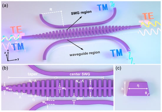
Figure 1.
Schematic of the proposed TE-pass polarizer on LNOI platform. (a) 3D view of the polarizer. (b) Geometrical parameters of the polarizer. (c) Cross-sectional view of the lithium niobate waveguide.
In the proposed polarizer, the TE and TM modes primarily propagate along the y-axis within the central SWG region and the upper/lower waveguide regions, therefore the Effective Medium Theory of the SWG and the optical waveguide properties of LN are the essential considerations. According to the EMT established by S. M. Rytov [32], SWGs with grating periods Λ much smaller than the incident wavelength λ (Λ ≪ λ) can be treated as homogeneous anisotropic media, allowing optical field propagation with negligible loss. The effective refractive indices of the SWG are given by Equation (2) [20,21]:
where no and ne denote the ordinary and extraordinary refractive indices of the SWG, while nLN and nSiO2 represent the refractive indices of LN and SiO2, respectively. For optical fields perpendicularly directed to the grating orientation, the anisotropic properties of the SWG can be described by the effective refractive index tensor shown in Equation (3) [20]:
Regarding the crystal orientation and the SWG optical axes in our device, the main electric field component of the TE mode is along the z-axis, while that of the TM mode is along the x-axis. In this case, both modes correspond to the ordinary refractive index (no) of the SWG, as defined in the tensor components of Equation (3).
Figure 2a illustrates the relationship between the equivalent refractive indices of the SWG and the duty cycle f as derived from Equation (2). In practical fabrication, an excessively high duty cycle may cause overlap between adjacent grating units due to the inherent sidewall inclination of LN waveguides, whereas an relatively large grating period may cause the grating to operate in the Bragg reflection regime, potentially increasing TE mode reflection and degrading the transmission efficiency [21,22,33]. To balance both manufacturability and optical performance, the design adopts a grating period of Λ = 0.36 μm, a duty cycle of f = 0.65, and a sidewall angle of θ = 75°, which were obtained through simulation and are consistent with the achievable precision of current micro/nanofabrication techniques.
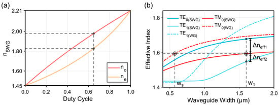
Figure 2.
(a) The relationship between equivalent refractive index of the SWG and the grating duty cycle. (b) Effective refractive indices of the guided modes versus waveguide width.
The phase-matching condition indicates that efficient modal coupling is realized when the TM0 modes in the central SWG region and the adjacent waveguides share identical effective refractive indices [34,35]. To verify this, the effective indices of TE and TM modes were systematically calculated as functions of waveguide width using the finite-difference eigenmode (FDE) solver, and the results are presented in Figure 2b. The simulations show that when the straight waveguide width is set to Ws = 0.575 μm and the SWG width to W1 = 1.60 μm, the TM0 modes in both structures exhibit identical effective indices (neff = 1.594), thereby satisfying the phase-matching condition. In this configuration, the effective index difference between TE0 and TM0 modes is Δneff1 = 0.0839, while that between TM0 and TE1 modes is Δneff2 = 0.0462; both Δneff values are sufficient to block TE-TM mode coupling and avoid mode hybridization. Accordingly, at the calculated values of W1 and Ws, the polarizer could achieve a relatively low IL alongside a high PER. Under these conditions, the TE0 mode does not satisfy the coupling requirement and is transmitted through the central SWG region with a small IL, whereas the TM0 mode is coupled into the adjacent waveguides and subsequently routed into bent sections with width Ws = 0.575 μm and radius R = 25 μm, where it is effectively filtered out from the central SWG. As a result, efficient separation between TE and TM polarizations is accomplished, enabling a high-performance TE-pass polarizer.
3. Results and Analysis
Following the above design principles, simulations were conducted to analyze the influence of structural parameters on the polarizer characteristics, as shown in Figure 3. The transmission efficiencies of TE and TM modes are strongly affected by both the magnitude and the variation rate of the SWG width in the tapered region, and the grating width must be carefully optimized to maximize TE0 mode transmission. To obtain the optimal width profile, four interpolation functions were systematically evaluated, including linear (W1), polynomial (W2, second-order), cosine (W3), and exponential (W4, first-order) variations, with their mathematical formulations provided in Equation (4):
where W denotes the width of the grating at position i (i = 1, 2, …, N), Wwg represents the width of the input waveguide, W1 is the width of the grating in the central SWG region, and N is the total number of gratings in the tapered section. Figure 3a depicts the progressive variation of the SWG width from Wwg to W1. The corresponding transmission behavior was subsequently analyzed using three-dimensional finite-difference time-domain (3D-FDTD) simulations, with the TE0 mode transmission under specific numbers of Nt and Nm (e.g., Nt = 40, Nm = 60) for each interpolation method presented in Figure 3b. It can be seen that the highest TE0 mode transmission efficiency is realized with cosine interpolation (W3). Such a performance enhancement is attributed to the derivatives at both the start and end points approaching zero, resulting in slow variation of the grating width at both ends and faster variation in the middle, thereby effectively minimizing the IL while maintaining adiabatic mode conversion between the input waveguide and SWG structure. Building on these results, the cosine interpolation scheme was adopted for implementing the tapered SWG width transition to optimize overall device performance.
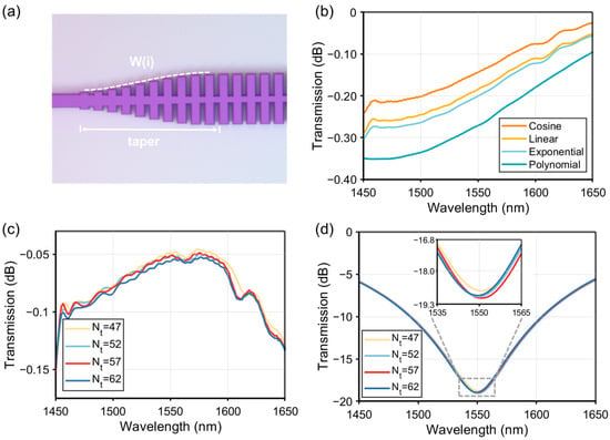
Figure 3.
(a) Evolution of the tapered SWG width based on interpolation functions. (b) TE0 mode transmission under various interpolation methods. (c) TE0 mode transmission for different Nt. (d) TM0 mode transmission for different Nt.
Furthermore, the performance of both TE0 and TM0 modes is also influenced by the number of SWG periods Nt in the tapered region. Figure 3c,d present the transmission characteristics of both modes for different Nt values. For the TE0 mode, the transmission exhibits a gradual decrease with increasing Nt, indicating that smaller values should be chosen to maintain a low IL. Conversely, the TM0 mode transmission initially decreases, reaching a minimum at Nt = 57, beyond which it gradually increases. Notably, reduced TM0 mode transmission enhances polarization selectivity but increases IL, hence a trade-off is required to determine the optimal Nt in the tapered region. On the basis of systematic optimization, Nt = 57 was identified as the optimal choice, ensuring a high PER while maintaining adiabatic transmission and low IL. To further improve TM0 mode coupling efficiency into the upper and lower waveguides, a particle swarm optimization (PSO) algorithm was employed to simultaneously optimize three key structural parameters: the number of gratings in the central SWG region Nm, the gap between the grating region and the waveguides, and the narrow-end width W0 of the tapered waveguide. After multiple iterative optimizations, the optimal parameters were determined to be Nm = 70, gap = 0.45 μm and W0 = 0.21 μm (satisfying the fabrication minimum feature size requirement of 0.2 μm).
An inverse design algorithm with shape optimization was applied to optimize the geometry of the upper and lower narrow-waveguide regions of the polarizer, aiming to mitigate the bandwidth limitation caused by the strong wavelength sensitivity of the directional coupler [36]. Owing to the structural symmetry along the propagation direction, the following analysis focuses on the lower waveguide section. This region consists of a central coupling waveguide with bent waveguides positioned on both sides. The coupling of the TM0 mode predominantly occurs within the central section, while the bent waveguides serve to further separate the coupled TM0 mode to prevent recoupling into the central grating region, allowing gradual attenuation during propagation. Accordingly, the optimization is focused on the coupling waveguide to broaden the bandwidth of the TM mode. Considering the small gap between the coupling waveguide and the SWG, shape optimization algorithms are constrained only to the outer side of the coupling waveguide to prevent structural dimensions below the fabrication limit.
To ensure the validity of the optimization process, the inverse design was initialized with parameters consistent with the preceding discussion: the number of central SWG periods Nm = 70, SWG width W1 = 1.6 μm, the gap between central SWG and waveguides of 0.45 μm, and the coupling waveguide width Ws = 0.575 μm. For the geometric parameterization of the coupling waveguide’s outer boundary, a third-order B-spline curve was introduced, providing not only a smooth profile but also continuous curvature transitions, which effectively minimizes scattering losses and adheres to the constraints of lithographic processes [37]. By placing n control points along the propagation axis, the boundary profile can be flexibly tuned for high local controllability. Specifically, the waveguide width is constrained within a predefined range prior to optimization. This ensures structural parameters remain above the minimum feature size to prevent both optical leakage and multi-mode interference, thereby maintaining single-mode operation and fabrication compatibility. To ensure structural continuity and mode matching during optimization, the first and last control points were constrained to Ws, consistent with the width of the bent waveguides which enhances device stability. In this work, a figure of merit (FOM) was defined as the optimization target for the inverse design, with its mathematical expression provided in Equation (5):
Here, TTE0 and TTM0 denote the transmission efficiencies of the TE0 and TM0 modes over a wavelength range of 1450–1650 nm. Within this span, transmissions are sampled with a 10 nm step and averaged to represent the overall efficiency. Since the transmission of both modes significantly impacts performance, equal weighting is assigned in Equation (5). The FOM ranges from 0 to 1, with higher values indicating greater transmission efficiency for the TE mode and stronger suppression of the TM mode. The adjoint method was utilized to efficiently calculate the gradients of the objective function with respect to all design variables through only two full-wave simulations per iteration [38]. By leveraging the adjoint-based gradient calculation, we can efficiently refine the B-spline boundaries. The sensitivity information is extracted via the overlap of forward and adjoint fields, ensuring that the optimization converges towards a geometry that aggressively suppresses the TM0 mode. The Limited-memory Broyden–Fletcher–Goldfarb–Shanno algorithm for Constrained optimization (L-BFGS-C) algorithm was adopted to iteratively update these variables to achieve performance improvement [39,40,41].
Figure 4a presents the optimized coupling waveguide profile obtained after 18 iterations with the number of control points set to n = 10, the corresponding figure of merit was FOM = 0.854 over the wavelength range of 1450–1650 nm (the FOM reaches a maximum value of 0.972 at 1550 nm), where the increase in TTM0 away from 1550 nm may reduce the averaged FOM across the bandwidth. Figure 4b shows a comparison of the TM0 mode transmission efficiency for both the initial and shape optimized structures. It can be observed that the inverse design not only reduced the TM0 transmission from −24.42 dB to −33.27 dB at 1550 nm, but also broadened the suppression bandwidth, which resulted in improved coupler efficiency and PER of the polarizer.
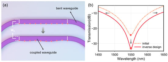
Figure 4.
(a) Comparison of the coupling waveguide structure. (b) Transmission efficiency of the TM0 mode corresponding to the initial and optimized designs.
Figure 5a illustrates the electric field distributions of the TE-pass polarizer under TE0 and TM0 mode excitations, where the TE0 mode mainly propagates through the central grating region without coupling, and the TM0 mode is gradually coupled from the central region into the upper and lower waveguides, resulting in polarization separation. Although the coupling efficiency of the TM0 mode was significantly optimized by the inverse design, a residual portion of the optical field away from 1550 nm remains confined in the central region without full coupling, which may constrain the bandwidth of the polarizer. For the polarizer, IL and PER constitute two critical performance parameters, with their definitions provided in Equation (6):
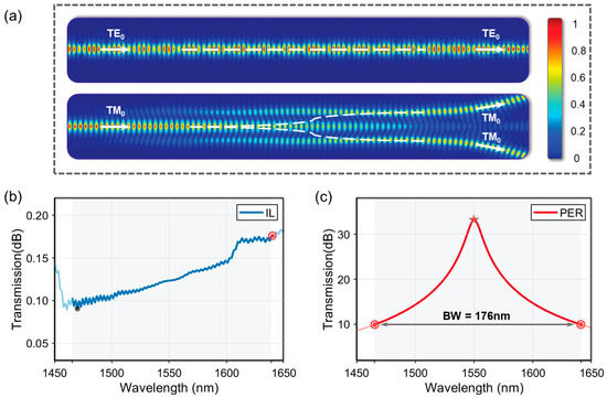
Figure 5.
Performance of the TE-pass polarizer. (a) Electric field distribution. (b) Insertion loss (IL). (c) Polarization extinction ratio (PER).
Here, TTE0 and TTM0 denote the transmission efficiencies of the TE0 and TM0 modes, respectively. The characteristics of IL and PER of the TE-pass polarizer are presented in Figure 5b,c. The proposed polarizer exhibits excellent performance with IL < 0.174 dB and PER > 10 dB over 176 nm (1465–1641 nm) bandwidth, effectively covering the S, C, and L bands. Within this range, the device maintains a PER > 20 dB over 55 nm (1522–1577 nm), and notably reaching a peak of 33.2 dB at 1550 nm.
4. Tolerance Analysis
This work provides a numerical proof of concept for the proposed TE-pass polarizer on the x-cut LNOI platform. To evaluate the experimental feasibility, it is essential to perform a fabrication tolerance analysis. First, the minimum feature size of the designed polarizer is 210 nm, which is well above the typical 200 nm resolution limit of current LNOI processing technologies. Second, potential discrepancies between numerical simulations and practical fabrication were investigated by simulating variations.
Figure 6 depicts the tolerance response of IL and PER to deviations in waveguide height h, SWG width W, and sidewall angle θ. For waveguide height h, a ±10 nm deviation has negligible impact on IL, with the PER showing a blue shift for Δh = −10 nm and a red shift for Δh = +10 nm. For SWG width, ΔW = −10 nm causes reduced IL and a red shift in PER, while ΔW = +10 nm produces higher IL along with a blue shift in PER. Alterations in the sidewall angle θ induce relatively minor changes in IL but a pronounced reduction in PER. These trends indicate that IL is more sensitive to width deviations, as they allow part of the TE0 mode to satisfy the phase-matching condition and couple into the grating, leading to an increased IL. Meanwhile, PER is more affected by variations in the sidewall angle due to associated changes in the SWG duty cycle. This modification alters the TM0 mode’s effective index, reducing coupling efficiency and consequently degrading PER performance.
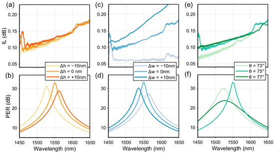
Figure 6.
Fabrication tolerance analysis of geometric parameters in the TE-pass polarizer. (a,b) Waveguide height h on IL and PER. (c,d) SWG width W on IL and PER. (e,f) sidewall angle θ on IL and PER.
The above results demonstrate that the device maintains a PER > 20 dB across the C-band within reasonable manufacturing tolerances. Furthermore, considering potential sidewall roughness and waveguide dimensional deviations in actual fabrication, we have optimized the effective waveguide width (η) during the simulation stage. This approach effectively mitigates the impact of fluctuations in waveguide width and sidewall slant on the grating period, thereby preventing significant performance degradation. Our analysis confirms that the proposed polarizer exhibits high tolerance to manufacturing imperfections and can operate stably within the range of practical experimental errors.
5. Conclusions
This work has designed and modeled an x-cut LNOI-based TE-pass polarizer employing SWG metamaterials. The polarizer consists of a central grating region and upper/lower waveguide sections. By designing the structural parameters of the SWG and applying an inverse design algorithm to optimize the coupling efficiency, the TE0 mode is transmitted through the polarizer with minimal loss, while the TM0 mode is efficiently coupled out of the SWG region. The polarizer achieves an IL < 0.174 dB and PER > 10 dB over a 176 nm bandwidth (1465–1641 nm), reaching a maximum PER value of 33.2 dB at 1550 nm. The device exhibits a total length of 66 μm and provides an operational bandwidth that covers the S, C, and L bands. A comparison of polarizer performance on the LNOI platform with previously reported devices is provided in Table 1. The proposed TE-pass polarizer combines ultra-low insertion loss, broad operational bandwidth, and compact device dimensions, offering competitive overall performance in comparison with previously reported LNOI-based polarizers. These characteristics suggest strong potential for applications in polarization control and mode conversion that are sensitive to IL and demand high stability, offering a promising technical pathway toward high-performance integrated polarization management and paving the way for future integration with devices like electro-optic modulators to fully exploit the performance of LNOI-based photonic systems.

Table 1.
Performance comparison of polarizers on the LNOI platform.
Author Contributions
Conceptualization, Y.L. (Yingyi Liu); methodology, Y.L. (Yingyi Liu), C.C., H.C. and Y.L. (Yang Lan); software, Y.L. (Yingyi Liu), C.C., H.C. and Y.L. (Yang Lan); data curation, Y.L. (Yingyi Liu); writing—original draft preparation, Y.L. (Yingyi Liu); writing—review and editing, Y.L. (Yingyi Liu) and X.F.; supervision, X.F. and L.Y. All authors have read and agreed to the published version of the manuscript.
Funding
This research received no external funding.
Data Availability Statement
The data presented in this study are available on request from the corresponding author.
Conflicts of Interest
The authors declare no conflicts of interest.
References
- Hou, S.; Hu, H.; Liu, Z.; Xing, W.; Zhang, J.; Hao, Y. High-Speed Electro-Optic Modulators Based on Thin-Film Lithium Niobate. Nanomaterials 2024, 14, 867. [Google Scholar] [CrossRef] [PubMed]
- Wang, D.; Liu, Y.; Xu, B.; Sun, W.; Jia, Z.; Zhu, S.; Zhu, N. Traveling Wave Electrode Simulation for Integrated Lithium Niobite Electro-optic Modulators; SPIE: Bellingham, WA, USA, 2021; Volume 11763. [Google Scholar]
- Yu, M.; Okawachi, Y.; Cheng, R.; Wang, C.; Zhang, M.; Gaeta, A.L.; Lončar, M. Raman lasing and soliton mode-locking in lithium niobate microresonators. Light Sci. Appl. 2020, 9, 9. [Google Scholar] [CrossRef] [PubMed]
- He, Y.; Yang, Q.-F.; Ling, J.; Luo, R.; Liang, H.; Li, M.; Shen, B.; Wang, H.; Vahala, K.; Lin, Q. Self-starting bi-chromatic LiNbO3 soliton microcomb. Optica 2019, 6, 1138–1144. [Google Scholar] [CrossRef]
- Zhang, B.; Li, S.; Chai, S.; Wu, X.; Ma, J.; Chen, L.; Li, Y. Nonlinear distortion and spatial dispersion of intense terahertz generation in lithium niobate via the tilted pulse front technique. Photon. Res. 2018, 6, 959–964. [Google Scholar] [CrossRef]
- Alibart, O.; D’Auria, V.; Micheli, M.D.; Doutre, F.; Kaiser, F.; Labonté, L.; Lunghi, T.; Picholle, É.; Tanzilli, S. Quantum photonics at telecom wavelengths based on lithium niobate waveguides. J. Opt. 2016, 18, 104001. [Google Scholar] [CrossRef]
- Chen, F. Photonic guiding structures in lithium niobate crystals produced by energetic ion beams. J. Appl. Phys. 2009, 106. [Google Scholar] [CrossRef]
- Hu, H.; Ricken, R.; Sohler, W. Lithium niobate photonic wires. Opt. Express 2009, 17, 24261–24268. [Google Scholar] [CrossRef]
- Poberaj, G.; Hu, H.; Sohler, W.; Günter, P. Lithium niobate on insulator (LNOI) for micro-photonic devices. Laser Photonics Rev. 2012, 6, 488–503. [Google Scholar] [CrossRef]
- Lin, J.; Bo, F.; Cheng, Y.; Xu, J. Advances in on-chip photonic devices based on lithium niobate on insulator. Photon. Res. 2020, 8, 1910–1936. [Google Scholar] [CrossRef]
- Zhang, J.; Cassan, E.; Zhang, X. Wideband and Compact TE-Pass/TM-Stop Polarizer Based on a Hybrid Plasmonic Bragg Grating for Silicon Photonics. J. Light. Technol. 2014, 32, 1383–1386. [Google Scholar] [CrossRef]
- Saitoh, E.; Saitoh, K.; Koshiba, M. Compact TE/TM-pass polarizer based on lithium niobate on insulator ridge waveguides. In Proceedings of the IEEE Photonics Conference 2012, Cocoa Beach, FL, USA, 23–27 September 2012; pp. 634–635. [Google Scholar]
- Zhang, L.; Zhang, L.; Fu, X.; Yang, L. Compact, Broadband and Low-Loss Polarization Beam Splitter on Lithium-Niobate-On-Insulator Using a Silicon Nanowire Assisted Waveguide. IEEE Photonics J. 2020, 12, 1–6. [Google Scholar] [CrossRef]
- Duan, S.; Chen, Y.; Li, G.; Zhu, C.; Chen, X. Broadband polarization beam splitter based on a negative refractive lithium niobate photonic crystal slab. Chin. Opt. Lett. 2016, 14, 042301. [Google Scholar] [CrossRef]
- Chen, Z.; Yang, J.; Wong, W.-H.; Pun, E.Y.-B.; Wang, C. Broadband adiabatic polarization rotator-splitter based on a lithium niobate on insulator platform. Photon. Res. 2021, 9, 2319–2324. [Google Scholar] [CrossRef]
- Wang, X.; Pan, A.; Li, T.; Zeng, C.; Xia, J. Efficient polarization splitter-rotator on thin-film lithium niobate. Opt. Express 2021, 29, 38044–38052. [Google Scholar] [CrossRef] [PubMed]
- Dai, S.; Yu, W.; Zhao, Y.; Li, M.; Li, J.; Zhang, Z.; Liu, J. Broadband and Compact TE-Pass Polarizer Based on Hybrid Plasmonic Grating on LNOI Platform. IEEE Photonics J. 2021, 13, 1–9. [Google Scholar] [CrossRef]
- Qi, L.; Chen, K.; Ruan, Z.; Chen, G.; Liu, L. TE-Pass Polarizer Based on Asymmetrical Directional Couplers on Thin-Film Lithium Niobate. In Proceedings of the 2022 Asia Communications and Photonics Conference (ACP), Shenzhen, China, 5–8 November 2022; pp. 1393–1395. [Google Scholar]
- Fei, Y.; Xu, Y.; Dong, Y.; Zhang, B.; Ni, Y. Reconfigurable TE-pass polarizer based on lithium niobate waveguide assisted by Ge2Sb2Te5 and silicon nitride. Appl. Opt. 2023, 62, 6499–6506. [Google Scholar] [CrossRef]
- Luque-González, J.M.; Sánchez-Postigo, A.; Hadij-ElHouati, A.; Ortega-Moñux, A.; Wangüemert-Pérez, J.G.; Schmid, J.H.; Cheben, P.; Molina-Fernández, Í.; Halir, R. A review of silicon subwavelength gratings: Building break-through devices with anisotropic metamaterials. Nanophotonics 2021, 10, 2765–2797. [Google Scholar] [CrossRef]
- Halir, R.; Bock, P.J.; Cheben, P.; Ortega-Moñux, A.; Alonso-Ramos, C.; Schmid, J.H.; Lapointe, J.; Xu, D.-X.; Wangüemert-Pérez, J.G.; Molina-Fernández, Í.; et al. Waveguide sub-wavelength structures: A review of principles and applications. Laser Photonics Rev. 2015, 9, 25–49. [Google Scholar] [CrossRef]
- Zhang, J.; Xu, L.; Mao, D.; D’Mello, Y.; Li, W.; Lessard, S.; Plant, D.V. All-silicon multi-band TM-pass polarizer on a 220 nm SOI enabled by multiplexing grating regimes. Opt. Express 2022, 30, 326–335. [Google Scholar] [CrossRef]
- Han, X.; Chen, L.; Jiang, Y.; Frigg, A.; Xiao, H.; Nguyen, T.G.; Boes, A.; Yang, J.; Ren, G.; Su, Y.; et al. Integrated Subwavelength Gratings on a Lithium Niobate on Insulator Platform for Mode and Polarization Manipulation. Laser Photonics Rev. 2022, 16, 2200130. [Google Scholar] [CrossRef]
- Xu, H.; Dai, D.; Shi, Y. Ultra-Broadband and Ultra-Compact On-Chip Silicon Polarization Beam Splitter by Using Hetero-Anisotropic Metamaterials. Laser Photonics Rev. 2019, 13, 1800349. [Google Scholar] [CrossRef]
- Halir, R.; Ortega-Moñux, A.; Benedikovic, D.; Mashanovich, G.Z.; Wangüemert-Pérez, J.G.; Schmid, J.H.; Íñigo, M.-F.; Cheben, P. Subwavelength-Grating Metamaterial Structures for Silicon Photonic Devices. In Proceedings of the IEEE 2018, Salt Lake City, UT, USA, 18–23 June 2018; Volume 106, pp. 2144–2157. [Google Scholar] [CrossRef]
- Li, C.; Zhang, M.; Xu, H.; Tan, Y.; Shi, Y.; Dai, D. Subwavelength silicon photonics for on-chip mode-manipulation. PhotoniX 2021, 2, 11. [Google Scholar] [CrossRef]
- Sun, L.; Zhang, Y.; He, Y.; Wang, H.; Su, Y. Subwavelength structured silicon waveguides and photonic devices. Nanophotonics 2020, 9, 1321–1340. [Google Scholar] [CrossRef]
- Chen, L.R.; Wang, J.; Naghdi, B.; Glesk, I. Subwavelength Grating Waveguide Devices for Telecommunications Applications. IEEE J. Sel. Top. Quantum Electron. 2019, 25, 1–11. [Google Scholar] [CrossRef]
- Liu, J.-M.; Zhang, D.-L. Ultra-broadband thin-film lithium niobate TM-pass waveguide polarizer using subwavelength grating metamaterial. Opt. Laser Technol. 2023, 164, 109556. [Google Scholar] [CrossRef]
- Han, X.; Cheng, R.; Huang, L.; Yu, P.; Feng, L.; Ren, G.; Mitchell, A.; Tian, Y.; Ren, X.; Xia, H. Ultra-broadband TM-pass polarizer based on anisotropic metamaterials in lithium niobate on an insulator. Opt. Lett. 2024, 49, 1774–1777. [Google Scholar] [CrossRef] [PubMed]
- Yang, Y.-K.; Guo, H.-J.; Chen, W.-B.; Qu, B.-A.; Yu, Z.-G.; Tan, M.-Q.; Guo, W.-T.; Liu, H.-F. High polarization extinction ratio achieved base on thin-film lithium niobate. J. Infrared Millim. Waves 2024, 43, 828. [Google Scholar] [CrossRef]
- Rytov, S.M. Electromagnetic Properties of a Finely Stratified Medium. Sov. Phys. JETP-USSR 1956, 2, 466–475. [Google Scholar]
- Liu, W.; Fu, X.; Cheng, C.; Yang, L. High-performance TM-pass polarizer based on anti-symmetric Bragg gratings. Opt. Express 2023, 31, 44148–44159. [Google Scholar] [CrossRef] [PubMed]
- Jiang, W.; Xie, L.; Zhang, L. Design and experimental demonstration of a silicon five-mode (de)multiplexer based on multi-phase matching condition. Opt. Express 2023, 31, 33343–33354. [Google Scholar] [CrossRef]
- Yusof, N.R.; Ali, N.; Kolenderski, P.; Słowik, K.; Endut, R.B.; Junid, S.A.A.S. Phase Matching in Microstructured Lithium Niobate on Insulator Waveguides. IEEE Access 2023, 11, 49035–49041. [Google Scholar] [CrossRef]
- Molesky, S.; Lin, Z.; Piggott, A.Y.; Jin, W.; Vucković, J.; Rodriguez, A.W. Inverse design in nanophotonics. Nat. Photonics 2018, 12, 659–670. [Google Scholar] [CrossRef]
- Khoram, E.; Qian, X.; Yuan, M.; Yu, Z. Controlling the minimal feature sizes in adjoint optimization of nanophotonic devices using b-spline surfaces. Opt. Express 2020, 28, 7060–7069. [Google Scholar] [CrossRef]
- Zhou, H.; Liao, K.; Su, Z.; Li, T.; Geng, G.; Li, J.; Wang, Y.; Hu, X.; Huang, L. Tunable on-chip mode converter enabled by inverse design. Nanophotonics 2023, 12, 1105–1114. [Google Scholar] [CrossRef] [PubMed]
- Cheng, C.; Yang, S.; Liu, W.; Liu, S.; Huo, Y.; Fu, X.; Yang, L. Ultra-Compact Inverse Designed Multimode Waveguide Bend Based on Levelset Method. IEEE Photonics Technol. Lett. 2024, 36, 571–574. [Google Scholar] [CrossRef]
- Yang, S.; Jia, H.; Niu, J.; Fu, X.; Yang, L. CMOS-compatible ultra-compact silicon multimode waveguide bend based on inverse design method. Opt. Commun. 2022, 523, 128733. [Google Scholar] [CrossRef]
- Liao, J.; Tian, Y.; Yang, Z.; Xu, H.; Dai, T.; Zhang, X.; Kang, Z. Broadband and Compact Silicon Multimode Waveguide Bends Based on Hybrid Shape Optimization. J. Light. Technol. 2024, 42, 4882–4891. [Google Scholar] [CrossRef]
Disclaimer/Publisher’s Note: The statements, opinions and data contained in all publications are solely those of the individual author(s) and contributor(s) and not of MDPI and/or the editor(s). MDPI and/or the editor(s) disclaim responsibility for any injury to people or property resulting from any ideas, methods, instructions or products referred to in the content. |
© 2026 by the authors. Licensee MDPI, Basel, Switzerland. This article is an open access article distributed under the terms and conditions of the Creative Commons Attribution (CC BY) license.