Abstract
Generative artificial intelligence (AI) models including GPT, Gemini, and DeepSeek are reshaping embodied agents, temporal prediction, and autonomous driving, demanding a ten-fold annual growth in training FLOPS that Moore’s law can no longer sustain. Consequently, scale-out GPU clusters require >400 Gb/s lane-rate optical interconnects within AI data-centers (AIDCs). Single-photodiode direct detection offers density, latency, and energy advantages, but DAC bandwidth remains limited to around 70 GHz. We present an optical triple-band multiplexing scheme that replaces high-frequency radio frequency (RF) mixers and local oscillators (LOs) with photonic components. A Mach–Zehnder modulator (MZM) generates 80-GBd PS-PAM-20 signal while an in-phase/quadrature (IQ) modulator driven by a wavelength-offset laser creates two independent 35-GBd PS-64-QAM bands. The proposed optical multiplexing method breaks conjugate symmetry and enhances dispersion tolerance of the direct detection system. After 200 m SSMF transmission and single 70-GHz photodiode (PD) detection, digital signal-signal beating interference (SSBI)/cross-beating compensation enables the recovery of net 543.9 Gb/s signal (line rate of 686.6 Gb/s) using only 45-GHz DACs. The optical multiplexing architecture provides a path to beyond-400 Gb/s lanes and demonstrates a scalable, energy-efficient solution for next-generation AI clusters.
1. Introduction
Generative artificial intelligence (AI), epitomized by large language models such as GPT, Claude, Gemini, and DeepSeek series, is rapidly reshaping modern computing. Its applications now span embodied agents that integrate vision, language, and robotic control [1,2]. These foundation models are trained on trillion-token corpora that demand tens of thousands of graphics processing units (GPUs) operating in tight synchrony for weeks or months. Consequently, AI data centers (AIDCs) have been transforming into globally distributed computing infrastructures. Traditional Dennard-scaling and Moore’s-law trends can no longer support a ten-fold annual increase in training FLOPS [3,4]. Consequently, architects adopt scale-out topologies that federate geographically distributed GPU islands through lossless, sub-microsecond-loss optical networks. Industry roadmaps indicate that single-lane data rates will exceed 400 Gb/s before 2027, pushing coherent optics, silicon-photonics co-packaging, and multi-mode vertical-cavity surface-emitting laser (VCSEL) arrays into the frontline of volume manufacturing [5]. High-speed optical interconnects can unlock sufficient memory-semantic bandwidth to fully utilize GPU tensor cores, reducing job completion time and energy per token and enabling future AI services to keep pace with rapidly growing user demand.
Conventional direct detection (DD) using a single photodiode (PD) provides a compact and cost-efficient solution for short-reach optical interconnects, particularly within intra-AIDC scenarios [6,7]. As summarized in [7], the absence of local oscillator (LO) and coherent 90° optical hybrid in DD schemes significantly reduces both complexity and energy consumption, satisfying the stringent requirements of AIDC networks for high density, low latency, and energy efficiency. Furthermore, DD systems can achieve improved spectral efficiency when higher-order modulation formats and low-complexity digital signal processing (DSP) algorithms are employed [8,9,10,11]. However, the capacity scaling obeys a logarithmic law that is constrained by the available signal-to-noise ratio (SNR). Once the SNR margin is exhausted, further capacity scaling is more effectively achieved by increasing the baud rate, that is, by expanding the signal bandwidth.
To extend the available bandwidth, numerous schemes employing multiplexing in either the electrical or optical domain have been introduced. As the electronic bandwidth scaling of digital-to-analog converters (DACs) lags behind steadily growing traffic demand, it has become a critical bottleneck for DD links. To circumvent this limitation, electrical multiplexing techniques are therefore adopted to surpass the effective bandwidth of a single DAC [12,13,14,15,16,17,18,19,20,21]. While electrical time-division multiplexing (ETDM) can double the sampling rate of DAC, the analog bandwidth is not significantly improved. In comparison, analog multiplexing (AMUX) [15,16,17,18] and digital band-interleaving (DBI) [13,14,19,20,21] suppress spectral aliasing [12] by splitting a broadband signal into parallel baseband DAC channels that are up-converted by radio frequency (RF) and merged into one waveform, yielding record net 651 Gb/s IM-DD [18] and 440-GBd bipolar PAM generation with spectrally sliced coherent detection [21]. Nevertheless, it should be noted that such electrical multiplexing schemes require meticulous design and precise integration of high-frequency RF mixers and oscillators that must operate over broad bandwidths while maintaining stringent phase-noise and linearity specifications.
Owing to their optical bandwidth far exceeding that of contemporary electronics, advanced broadband electro-optic modulators have become the key enablers of advanced optical multiplexing. For instance, a thin-film lithium niobate (TFLN) modulator has demonstrated exceptional performance, achieving a record 1.96 Tb/s net data rate with a sub-1 V drive voltage, 110 GHz bandwidth, and an ultralow power consumption of 1.04 fJ/bit [22]. Similarly, a silicon photonic (SiP) modulator utilizing a novel P–N dual-drive scheme realizes 200-GBaud operation through intrinsic signal processing capabilities, offering complementary metal oxide semiconductor (CMOS) compatibility and a power efficiency of 2.5 pJ/bit [23]. In the same vein, an InP electro-absorption modulated laser offering >110-GHz bandwidth has been used to transmit 540 Gb/s (180 GBaud PAM-8) over 30 km standard single-mode fiber (SSMF) [24].
These high-performance modulators render optical multiplexing techniques an attractive route to expanding the available system bandwidth. Carrier-suppressed return-to-zero optical time-division multiplexing (CSRZ-OTDM) has employed a single-carrier net rate of 2.59 Tb/s by integrating a 224 GBaud transmitter with an 8 × 4 digital calibrator that cancels spurious distortions [25]. Alternatively, an on-chip optical spectrally sliced synthesis scheme implemented on a TFLN platform coherently combines two spectral slices driven by lower-speed DACs, generating single-carrier signals at symbol rates up to 256 GBaud and line rates of 2 Tb/s, thereby circumventing the conventional electronic bandwidth bottleneck [26].
In this work, we leverage the concept of optical band multiplexing to achieve high-speed direct detection for intra-AIDC interconnects using low-bandwidth DACs. Instead of relying on RF mixers and LOs, the proposed method utilizes a single intensity modulator to create the low-frequency sub-band and a single in-phase/quadrature (IQ) modulator driven by a second laser whose wavelength is relatively offset to generate the medium- and high-frequency sub-bands, thereby removing the need for any electronic frequency translation stage. Thanks to optical multiplexing, the composite optical field is no longer constrained by the conjugate symmetry inherent to electrical band-interleaving. Heterodyne beating performed directly in the optical domain therefore imparts improved resilience against dispersion-induced power fading, at the expense of one additional electro-optic modulator. In the proof-of-concept experiment, we optically multiplex an 80-GBd probabilistically shaped 20-level pulse-amplitude-modulation (PS-PAM-20) signal with two independent 35-GBd PS 64-ary quadrature-amplitude-modulation (PS-64-QAM) signals based on 45-GHz DACs, achieving an aggregate line rate of 686.6 Gb/s and a net bit rate of 543.9 Gb/s.
This paper is an extension of our work presented at Asia Communications and Photonics Conference (ACP) 2025 [27]. Here we provide a more comprehensive evaluation of the robustness and scalability of the proposed optical triple-band multiplexing scheme. Specifically, we have provided a more detailed formula derivation for the mutual interference between the sub-bands generated from different laser sources. Additionally, we have added detailed simulation studies to explore the impact of signal-signal beating interference (SSBI) and cross-beating interference on the performance of the system, verifying the effectiveness of the proposed compensation algorithm. Then, we investigated the trend of the system as a function of signal-to-noise ratio (OSNR).
The remainder of this paper is structured as follows. Section 2 formulates the fundamental principles of the optical triple-band multiplexing scheme. Section 3 provides numerical results together with a quantitative analysis and verifies the efficacy of the proposed compensation algorithm in suppressing both impairments. Section 4 describes the experimental configuration and the complete DSP chain. Section 5 showcases the experimental results. A detailed comparative analysis of electrical multiplexing and optical multiplexing is presented in Section 6, along with the introduction of an alternative optical scheme. Finally, the conclusions are drawn in Section 7.
2. Principle
Figure 1a displays the operational principle of electrical band multiplexing based on digital-band-interleaving (DBI) technique. The target DBI waveform is composed of three mutually independent sub-bands, whose bandwidths are denoted , , and , respectively. Band 1 is retained at baseband. Band 2 is up-converted by a RF LO operating at frequency , producing an upper sideband (USB) located in the interval [, ] together with an undesired lower sideband (LSB) image. Both the image and the residual LO are suppressed by a sharp high-pass filter (HPF) after the mixer. Similarly, sub-band 3 is translated to an intermediate frequency by another RF LO set at , and a subsequent HPF selects the desired LSB spanning [, ], while rejecting the residual LO and the complementary LSB. The three conditioned sub-bands are finally combined by a mixer, and the aggregate electrical drive is applied to a wideband Mach–Zehnder modulator (MZM) to yield an intensity-modulated optical signal whose base-band spectrum extends over . Nevertheless, such electrical multiplexing schemes approach considerable hardware complexity, particularly in the design and monolithic integration of high frequency RF mixers and oscillators.
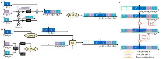
Figure 1.
(a) Working principle of electrical band multiplexing based on digital-band-interleaving (DBI) technique. B1/2/3: bandwidth of band 1/2/3; (·)*: conjugate; IM Mod.: intensity-modulation modulator. (b) Working principle of optical triple-band multiplexing. SCM: subcarrier multiplexing; IQ Mod.: in-phase/quadrature modulator; OC: optical coupler. (c) Signal evolution after direct detection with optical band multiplexing. : modulus operation; : square-root operation; /: division operation.
In comparison, the working principle of the proposed optical triple-band multiplexing scheme is illustrated in Figure 1b, beginning with signal generation at the transmitter. The process starts with electro-optical conversion: the baseband waveform with bandwidth drives a MZM to impress band 1 onto an optical carrier centered at frequency . In contrast to our previous work [28] that employed an additional intensity modulator, band 2 and band 3 are now jointly modulated by an IQ modulator, thereby further releasing the bandwidth requirement on the DACs. Before reaching the IQ modulator, two independent baseband signals and , with bandwidths of and , respectively, are subcarrier multiplexed to form a complex-valued double-sideband (DSB) signal. The electro-optical conversion of the DSB signal is then completed by injecting a laser with another wavelength into the IQ modulator. To prevent spectral overlap in the optical domain, the operating center-frequency spacing () between the two lasers must satisfy the condition of . After an independent electro-optical modulation, the three optical sub-bands are combined by a 2 × 1 optical coupler (OC), yielding an ultra-high-bandwidth optical signal whose total field is expressed as
where is the square root operation reflecting power modulation by the intensity modulator biased at the quadrature point. In contrast, the IQ modulator is biased slightly above the null point to perform field modulation, thereby producing the dual-band subcarrier-multiplexed signal. Consequently, the proposed optical band multiplexing approach eliminates the need for high-bandwidth RF amplifiers and mixers at the cost of an extra modulator. Because the optical signal is no longer constrained by the conjugate symmetry inherent to electrical band-interleaving, its tolerance to dispersion-induced power fading is improved. It should also be noted that, if the relative phase between the two modulator branches is actively locked, the scheme can generate a true single-carrier waveform [29].
At the receiver, only a single-ended PD is employed for the reception of the wideband optical signal. Fiber dispersion is omitted here to facilitate an analytical treatment. After the square-law detection, the output photocurrent can be written as
where denotes for real part. Expanding in a Taylor series gives with coefficients and for . Hence the output photocurrent can be expressed as
where the 1st term is a direct current (DC) component, the 2nd term presents the linear term of at baseband, the third is the linear beating term of and centered at the intermediate frequency , the fourth describes the cross-beating interference imposed by on the other bands, and the fifth denotes the SSBI arising from bands 2 and 3. For the sake of simplicity, the photodiode responsivity is set to 1. Thanks to the optical multiplexing, the conjugate symmetry inherent to intensity-modulated signals in DBI is broken, thereby improving the tolerance of the system to chromatic dispersion (CD).
Figure 1c shows the demodulation procedure of the optical triple-band multiplexing scheme after direct detection. To reconstruct and mitigate the SSBI, the high-frequency bands (band 2 and 3) are firstly isolated by a digital high-pass filter, followed by a square operation, and subtracted from band 1. Once band 1 has been cleaned, the intensity-modulated waveform is recovered as , where is an additive digital carrier component whose value is set to match the carrier-to-signal power ratio (CSPR) condition in the optical domain. Here CSPR is defined as the power ratio between the optical carrier in band 1 and the total signal power of bands 1, 2, and 3. Cross-beating interference is subsequently compensated by the division operation, after which the three bands are fed into parallel signal demodulation modules for symbol decoding.
In practical implementation, the frequency response of the optical-to-electrical front-end in the receiver, comprising both the photodiode and the sampling oscilloscope, must be compensated at the first stage. Theoretically, the received photocurrent is expressed as
where is the convolution operation, and are the impulse response of the transmitter and receiver, respectively. While introduces a linear distortion, affects the squared field and therefore acts nonlinearly on the data. To improve the accuracy of subsequent SSBI and cross-beating mitigation, we firstly compensate the receiver response with a proposed low-complexity polynomial fitting algorithm applied directly in the frequency domain [28]. The compensated waveform is obtained as
where is the frequency in Hz, and and are the fitting coefficients chosen to approximate the inverse frequency response of .
3. Simulation Analysis
Numerical simulation was performed to characterize the proposed optical triple-band multiplexing scheme. At the transmitter, for the signal on band 1, we adopted 80-GBd PS-PAM-20 format with a fixed source entropy of 4.0 bits/symbol, which transmits the real and imaginary parts of a 400-QAM constellation. Here the 400-QAM constellation is truncated from a 1024-QAM template. The optical carrier was added by biasing the MZM at the quadrature point. As for the signal on band 2 and 3, we generate two independent 35-GBd PS-64-QAM symbol sequences and subcarrier multiplex them with a guard band of 1.6 GHz in the digital domain. Both of the two bands have a source entropy of 5.7 bits/symbol. A digital pilot tone was embedded between the spectra of band 2 and band 3 to emulate a residual carrier and to facilitate receiver-side frequency offset estimation (FOE) and carrier phase recovery (CPR). The frequency spacing between two lasers was fixed as 77.5 GHz. The OSNR was set at 50 dB, which includes the power of both optical carrier and digital pilot tone. After receiver-side DSP, the normalized generalized mutual information (NGMI) was calculated as the performance metric [30].
We first quantified the influence of carrier-to-signal power ratio (CSPR) of the intensity modulated signal (band 1) on system performance in Figure 2a. For all three bands, the NGMI first improves and then degrades as CSPR increases. A lower CSPR introduces strong nonlinear distortion, whereas a high CSPR reduce the effective SNR. Consequently, a CSPR of 20 dB is selected as optimum, maximizing the NGMI of band 1 while maintaining excellent performance for band 2 and 3. The benefit of SSBI-mitigation algorithm described in Section 2 is evident from the comparison between compensated and uncompensated curves in Figure 2a. At low CSPRs, the algorithm yields a larger gain for band 1, where nonlinearity is more pronounced. The improvement to other bands is relatively limited, and virtually negligible for band 3, which is consistent with its low level of cross-beating interference.
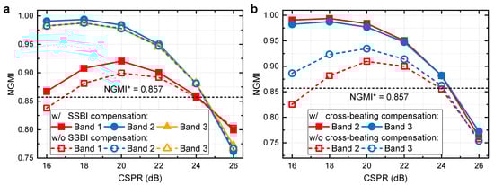
Figure 2.
(a) Carrier-to-signal power ratio (CSPR) optimization of band 1 with (w/) and without (w/o) signal-signal beating interference (SSBI) compensation. (b) Carrier-to-signal power ratio (CSPR) optimization of band 1 with (w/) and without (w/o) cross-beating interference compensation. Dashed line: NGMI threshold (i.e., NGMI*) of 0.857.
Figure 2b displays the influence of CSPR of band 1 on NGMI performance of bands 2 and 3. In the absence of cross-beating interference compensation, both medium- and high-frequency sub-bands (i.e., band 2 and 3) exhibit the same trend with increasing CSPR that is observed for band 1, and band 3 consistently outperforms band 2 across the entire 16–26 dB CSPR range, indicating that band 2 is more susceptible to nonlinear SSBI distortion. Enabling the digital compensation algorithm to raise the NGMI of both bands, removing the performance gap and yielding essentially identical results, thereby validating the effectiveness of the proposed interference-cancelation scheme.
When the CSPR is lower than 18 dB, the performance of each band begins to degrade, even with SSBI and cross-beating compensation applied. This was attributed to the coupling effect between the residual SSBI and the cross-beating terms. Because the SSBI compensation algorithm treats as a perturbation term, an assumption that becomes increasingly invalid under relatively low-CSPR conditions. Consequently, the inaccurate reconstruction of band 1 results in incomplete compensation of the cross-beating distortion associated with . Note that the CSPR requirement is associated with the peak-to-average power ratio (PAPR) of the signal waveform. So, one possible solution is to apply amplitude clipping the suppress the PAPR of the signal or to simply adopt lower modulation formats.
To emulate the residual carrier produced by the IQ modulator when it is biased slightly above the null point, we spectrally inserted a digital pilot tone between band 2 and 3. The pilot tone-to-signal power ratio (PTSPR) was defined as the pilot tone power divided by the combined power of band 2 and 3. Figure 3a quantifies system performance versus PTSPR. Thanks to the heterodyne detection, the performance of the bands 2 and 3 was insensitive to PTSPR, so the power of the residual carrier could be very small, reducing power consumption and SNR penalty. An PTSPR of −15 dB is therefore adopted. The figure also reveals that cross-beating-interference compensation yields a larger benefit for band 2, corroborating that band 2 experiences the more severe nonlinear distortion, as was anticipated.
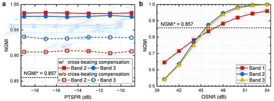
Figure 3.
(a) Pilot tone-to-signal power ratio (PTSPR) optimization of band 2/3 with (w/) and without (w/o) cross-beating interference compensation. (b) Normalized generalized mutual information (NGMI) as a function of optical signal-to-noise ratio (OSNR) for three bands. Dashed line: NGMI threshold (i.e., NGMI*) of 0.857.
Figure 3b presents the NGMI as a function of OSNR for the three sub-bands. To achieve the NGMI threshold of 0.857, band 1 requires a minimum OSNR of approximately 47 dB, whereas band 2 and 3 relax this requirement by about 1 dB. At a 50 dB OSNR, an attainable value in short-reach amplifier-less intra-data-center links where the optical carrier power is included; the measured NGMI values are 0.920, 0.977, and 0.977 for bands 1, 2 and 3, respectively.
4. Experimental Setup and DSP Stacks
4.1. Experimental Setup
Figure 4a illustrates the experimental configuration of the high-speed optical interconnects that employs the proposed optical triple-band multiplexing scheme. At the transmitter, an external cavity laser (ECL, EXFO, Quebec City, QC, Canada) emitting at 1549.79 nm with a linewidth of 100 kHz served as the optical source for band 1. Its output was intensity-modulated by a 40 GHz Mach–Zehnder modulator (MZM, EOspace Inc., Redmond, WA, USA) biased at the quadrature point, which generated the optical carrier and ensured linear modulation of band 1. The electrical drive for band 1 was supplied by the first channel of a 120 GSa/s arbitrary waveform generator (AWG, Keysight M8194A, Keysight Technologies, Santa Rosa, CA, USA) with an analog bandwidth of 45 GHz and boosted by a 50-GHz electrical amplifier (EA, SHF 807, SHF Communication Technologies AG, Berlin, Germany). Band 2 and band 3 were modulated onto another optical carrier from second ECL operating at 1549.17 nm, corresponding to a 76-GHz frequency spacing relative to the first carrier. This laser fed a 27-GHz 3 dB bandwidth IQ modulator (EOspace Inc., Redmond, WA, USA) whose bias was set slightly above the null point to produce a residual optical carrier with CSPR of approximately −15 dB. Channels 2 and 3 of the AWG jointly generate the dual-band subcarrier-multiplexed waveform containing band 2 and 3 for the IQ modulator. The three optical sub-bands were combined with aligned polarization states using a 50:50 optical coupler (Advanced Fiber Resources, Hong Kong, China).
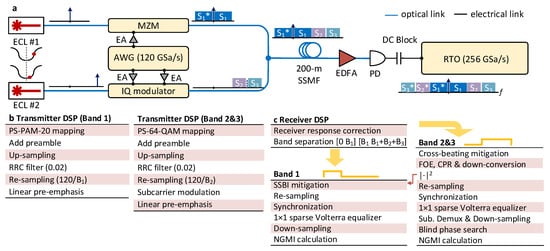
Figure 4.
(a) Experimental setup. (b) Transmitter- and (c) receiver-side DSP stacks. ECL: External cavity laser; AWG: arbitrary waveform generator; MZM: Mach-Zehnder modulator; EA: electrical amplifier; SSMF: standard single-mode fiber; EDFA: Erbium-doped fiber amplifier; PD: photodiode; DC: direct current; RTO: real-time oscilloscope; PS: probabilistic shaped; RRC: root-raised cosine; SSBI: signal-signal beating interference; FOE: frequency offset estimation; CPR: Carrier phase recovery; Sub. Demux: subcarrier demultiplexing; NGMI: normalized generalized mutual information. (·)*: conjugate.
The signal was transmitted over a 200 m SSMF that emulated an intra-data-center link. At the receiver, an erbium-doped fiber amplifier (EDFA, Amonics, Hong Kong, China) boosted the optical power to 9 dBm before the light was converted to the electrical domain by a 70 GHz photodiode (Finisar XPDV3120, Coherent Corp. (formerly Finisar), Fremont, CA, USA). We placed a 67-GHz DC block to fully utilize the quantization bits of the scope. Finally, A 256-GSa/s real-time oscilloscope (Keysight Technologies, Santa Rosa, CA, USA) digitized the waveform, and the captured data were processed offline.
4.2. DSP Stacks
At the transmitter, as shown in Figure 4b,c, the DSP sequence begins by mapping the payload bits allocated to band 1 onto a PS-PAM-20 constellation. We chose this modulation format to exploit the relatively higher SNR at a low-frequency region and therefore maximized the overall bitrate. Next, a 2048-symbol preamble was added for receiver-side frame synchronization and channel equalization. Both symbol sequences were then up-sampled and shaped with a root-raised-cosine (RRC) filter having a roll-off of 0.02. For band 1, the waveform was re-sampled to match the sampling rate of AWG and passed through a linear pre-emphasis FIR filter to pre-compensate for the transmitter-side bandwidth limitation. For bands 2 and 3, the bits assigned to bands 2 and 3 was mapped onto a PS-64-QAM constellation. The frame included a 4096-symbol preamble. After the RRC shaping and re-sampling, the signals were subcarrier-multiplexed to form a double-sideband spectrum, followed by a linear pre-emphasis stage. A 1.6-GHz guard band was inserted at the baseband to prevent corruption of the residual-carrier component by the signal spectrum.
At the receiver, the electrical waveform captured by the 256 GSa/s real-time oscilloscope was first passed through a polynomial-based receiver-response-correction filter that lifted up the 70 GHz photodiode and front-end amplifier frequency dependence. The corrected signal was then separated by using a digital brick-wall filter with a cut-off frequency of 41 GHz. For the low-band (band 1), we first reconstructed the SSBI by digitally squaring the simultaneously detected band 2 and 3 and subtract this estimate in two iterative steps. The cleaned waveform was then re-sampled to 2 samples per symbol (SPS) and synchronized according to cross-correlation with the embedded preamble. A sparse Volterra nonlinear equalizer was utilized to suppresses the residual inter-symbol interference (ISI) and modulation nonlinearity of the IM and IQ modulators. The tap length of the 1st-, 2nd-, and 3rd-order kernels were 361, 29, and 13, respectively. Finally, NGMI was computed to quantify performance. For the high-band pair (bands 2 and 3), cross-beating interference was removed by dividing the recovered optical field with the cleaned band 1. FOE and CPR exploited the residual carrier component [31]. After frame synchronization, a second sparse Volterra equalizer (tap lengths 201, 29, 13) mitigated joint ISI and beating distortion. Sub-carrier demultiplexing and down-sampling were followed by blind phase search (BPS) [32] to eliminate any residual phase error, after which NGMI was again evaluated. We can calculate the line rate and net data rate as [30]
where denotes the source entropy of band , is the baud rate of band , is the code rate, and is the bit number of each symbol in band .
5. Experimental Results
5.1. Optical Spectrum
Figure 5 presents the measured optical spectrum of the transmitted triple-band signal, recorded with a resolution of 0.01 nm. Band 1 is centered at approximately 1549.79 nm, while bands 2 and 3 are jointly located at 1549.17 nm. To combat the S21 response of the receiver, the power spectral density of bands 2 and 3 was intentionally enhanced compared to band 1. The two main strategies were to align the power spectral density of each band either in the optical or received electrical spectrum. In this experiment, we grouped the power levels of band 2 and 3 to make a partial pre-emphasis as a trade-off between complexity and performance. The inter-band crosstalk was maintained below −30 dB across the entire spectral range, indicating effective optical band multiplexing and minimal inter-band interference.
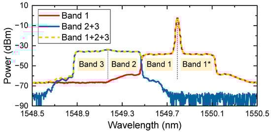
Figure 5.
Measured optical spectra of transmitted signals at 0.01 nm resolution. (·)*: conjugate.
5.2. Data Rate Optimization
We first maximized the data rate of band l by sweeping its source entropy. Figure 6a presents the measured NGMI of band 1 as its line rate is increased while the line rates of band 2 and 3 are held constant at 195.7 Gb/s and 162.8 Gb/s, respectively. A monotonic decline in NGMI was observed with increasing throughput of band 1. At the NGMI threshold of 0.857, the maximum achievable source entropy was 4.0 bits/symbol. The corresponding line rate was 321.3 Gb/s. Considering the code rate of 0.826 [30], this yields a net bit rate of 251.7 Gb/s for band 1. Throughout the sweep, the NGMI values of bands 2 and 3 remained initially stable and then decreased slightly, attributed to residual imperfections in the cross-beating interference compensation.
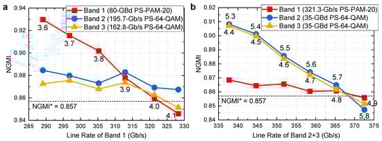
Figure 6.
(a) Measured NGMI versus line rate of band 1 after 200 m SSMF transmission. Band 1 is 80-GBd PS-PAM-20 signal with varying source entropy. Band 2 and 3 are fixed as 195.7 Gb/s and 162.8 Gb/s PS-64-QAM signals. (b) Measured NGMI versus line rate of band 2 and 3 after 200 m SSMF transmission. Band 1 is fixed as 321.3 Gb/s PS-PAM-20 signal. Band 2 and 3 are 35-GBd PS-64-QAM signals with varying source entropy. Dashed line: NGMI threshold (i.e., NGMI*) of 0.857.
Figure 6b summaries the NGMI measurements obtained when the line rate of band 1 was fixed at 321.3 Gb/s and the aggregate throughput of bands 2 and 3 was swept jointly. The NGMI of both high-frequency bands decreased monotonically with increasing line rate, while that of band 1 remained relatively flat. At the NGMI threshold of 0.857, the source entropies reached 5.7 bits/symbol for band 2 and 4.7 bits/symbol for band 3, corresponding to line rates of 199.0 Gb/s and 166.3 Gb/s, respectively. In contrast to the trend observed in Figure 3, the stable NGMI of band 1 confirms the effectiveness of the digital SSBI-mitigation scheme.
Figure 7 quantifies the individual contribution of each optical sub-band to the aggregate data rate. The measured line rates are 321.3 Gb/s (band 1), 199.0 Gb/s (band 2) and 166.3 Gb/s (band 3). The progressive decrease with band index is attributed to the roll-off of the receiver’s electro-optic response at higher frequencies. Applying a code rate of 0.826 (NGMI threshold 0.857) [30], the net bitrates become 251.7 Gb/s, 162.5 Gb/s and 129.7 Gb/s for bands 1–3, yielding a total net bitrate of 543.9 Gb/s. Figure 7i–iii present the corresponding recovered constellations: band 1 (PS-PAM-20) is rendered as a complex field by pairing odd- and even-time slots, while bands 2 and 3 (PS-64-QAM) exhibit clearly separated symbol clusters with no visible overlap. Due to the stringent SNR requirement of high-order modulation format, the receiver sensitivity is limited to 9 dBm.
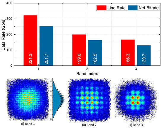
Figure 7.
Line rates and net bitrates versus band index. (i)–(iii) Recovered constellations of the signals on band 1, 2, and 3, respectively.
6. Discussions
6.1. Comparison of Electrical Multiplexing and Optical Band Multiplexing
In commercial systems, a CMOS DAC is typically used to drive an optical modulator for signal generation. However, under the electronic-bandwidth bottleneck, a single CMOS DAC struggles to produce wideband signals. Electrical multiplexing overcomes this limitation by digitally combining multiple sub-bands, introducing an electrical multiplexing front-end between the sub-DACs and the modulator. For an -fold bandwidth extension, this architecture requires sub-DACs, one electrical multiplexing front-end, and one electro-optic (E/O) modulator.
Alternatively, optical band multiplexing allows each sub-band from the sub-DACs to directly modulate on separate optical paths and then combine. This approach also uses sub-DACs, E/O modulators, and one optical coupler.
Both electrical and optical approaches can enable scalable bandwidth expansion. The comparison of ultra-high-speed experimental demonstrations using electrical/optical multiplexing schemes are illustrated in Table 1. Notably, electrical and optical multiplexing techniques differ in hardware trade-offs—particularly the need for high-frequency mixers and drivers on the electrical side, and the associated E/O modulators. With the rapid development of wideband, power-efficient TFLN technology, integrating multiple parallel E/O modulators on a single photonic chip may substantially reduce system cost while supporting further scaling.

Table 1.
Comparison of ultra-high-speed experimental demonstration using electrical/optical multiplexing schemes.
The concept of optical band multiplexing can also be applied to single-carrier signal generation, provided that the optical sources driving different E/O modulators are phase-coherent. In this context, optical frequency combs are well suited, as their stable line spacing and inherent phase coherence naturally satisfy these requirements. With comb-based optical sources, the phase-related DSP blocks, including FOE and CPR, can be removed at the receiver to reduce the power consumption.
Moreover, a single IQ modulator can in principle be employed for bandwidth extension. From the perspective of hardware complexity, however, an additional laser source is still required to provide an optical carrier at the edge of the signal spectrum in order to construct a single-sideband (SSB) signal. Furthermore, assuming that the electrical bandwidth of the DAC is limited to , a single IQ modulator can at most extend the available bandwidth to . In contrast, the proposed IM–IQ modulator configuration enables triple-band multiplexing with an effective bandwidth of , corresponding to a potential increase of approximately 50% in the achievable bitrate.
6.2. Alternative Scheme of Optical Band Multiplexing
To avoid the cross-beating impairment, an alternative implementation scheme of optical multiplexing is to exploit the polarization dimension. As shown in Figure 8, bands 2 and band 3 are combined with band 1 through a polarization-beam combiner. In such a configuration, the transmitted optical field in Jones space is
where is the optical carrier on X polarization generated by the quadrature point of MZM, and is the optical carrier on Y polarization from the optical source of band 1, which aims to generate the linear beating term of band 2 and band 3.
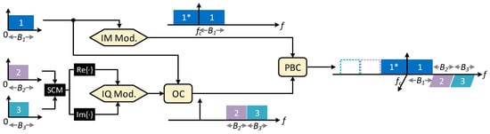
Figure 8.
Alternative scheme of optical triple-band multiplexing. SCM: subcarrier multiplexing; IQ Mod.: in-phase/quadrature modulator; OC: optical coupler. PBC: polarization-beam combiner. (·)*: conjugate.
At the receiver, the output photocurrent after the square-law detection can be written as
where and are DC components. By assigning band 1 and bands 2/3 to orthogonal polarizations, cross-beating distortion is effectively suppressed. As a result, the reception of bands 2/3 becomes linear, analogous to heterodyne detection. The cost is the increased hardware complexity at the transmitter side.
6.3. Impact of Fiber Dispersion
We further evaluated the fiber dispersion tolerance of the proposed optical triple-band multiplexing scheme through numerical simulations. In the simulation, band 1 employs an 80-GBd PS-PAM-20 format with a source entropy of 4.0 bits/symbol, while bands 2 and 3 are modulated using two independent 35-GBd PS-64-QAM signals, each with a source entropy of 5.7 bits/symbol.
As shown in Figure 9, the NGMI performance of bands 2 and 3 remains nearly unaffected as the transmission distance increases. This behavior can be attributed to the fact that these two bands are generated as complex-valued single-sideband signals and therefore do not possess conjugate sidebands, rendering them inherently resistant to dispersion-induced power fading. In contrast, band 1 is generated via intensity modulation, and its NGMI performance degrades significantly when the fiber length exceeds approximately 1.5 km.
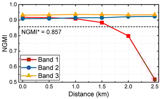
Figure 9.
Simulated NGMI of band 1/2/3 versus fiber length. Dashed line: NGMI threshold (i.e., NGMI*) of 0.857.
Using an NGMI threshold of 0.857, a transmission distance of 1.0 km is sufficient to fully cover the targeted intra-AIDC application scenario. It should be noted that the simulation is conducted assuming C-band transmission with a chromatic dispersion parameter of 17 ps/nm/km. This condition is equivalent to approximately 8 km of transmission at the longest wavelength of LAN-WDM channels, owing to the reduced dispersion coefficient in that wavelength range.
6.4. Impact of Laser Phase Noise
We characterized the laser phase noise tolerance of the optical triple-band multiplexing scheme through numerical simulations. We still used an 80-GBd PS-PAM-20 format (4.0 bits/symbol source entropy) for band 1, and two independent 35-GBd PS-64-QAM signals (5.7 bits/symbol source entropy) for bands 2 and 3. The laser phase noise is modeled as a Wiener process, whose variance is . Here is the combined linewidth of both laser 1 and laser 2 in Figure 4, and is the time interval of the simulation, which operates at the sampling rate of 240 GSa/s.
As shown in Figure 10, the NGMI performance of band 1 remains unchanged over a wide range of laser linewidths. This behavior arises because band 1 follows a conventional IM-DD configuration, in which the optical phase noise is completely removed after the square-law detection of the photodiode.
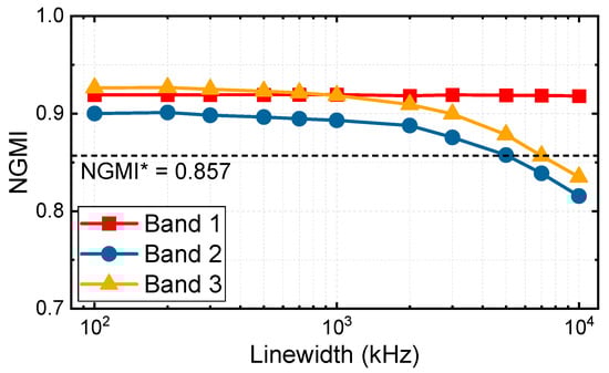
Figure 10.
Simulated NGMI of band 1/2/3 versus combined laser linewidth. Dashed line: NGMI threshold (i.e., NGMI*) of 0.857.
In contrast, bands 2 and 3 rely on heterodyne-like detection and are therefore susceptible to laser phase noise. Fortunately, the presence of residual optical carrier enables accurate and continuous phase tracking, which effectively mitigates phase-noise-induced degradation. As a result, the NGMI performance remains nearly constant for a combined laser linewidth of up to 1 MHz. Furthermore, using an NGMI threshold of 0.857, a combined linewidth of approximately 5 MHz can still be supported, demonstrating the feasibility of deploying low-cost lasers in the proposed system.
7. Conclusions
In this paper, we propose and experimentally validate an optical triple-band multiplexing method that overcomes the intrinsic bandwidth ceiling of DACs without resorting to high-frequency RF mixers or LOs. The scheme optically combines an 80-GBd PS-PAM-20 signal from an intensity modulator together with two independent 35-GBd PS-64-QAM sub-bands from an IQ modulator. Single-photodiode direct detection after 200 m SSMF followed by digital SSBI and cross-beating interference mitigation achieves an aggregate line rate of 686.6 Gb/s and a net bit-rate of 543.9 Gb/s. The receiver employs only commercial 45-GHz DACs and a 70-GHz photodiode, demonstrating that the approach is immediately compatible with volume CMOS platforms. These results verify that optical band multiplexing offers a scalable and energy-efficient route towards beyond-400 Gb/s lane-rate optical interconnects for next-generation intra-data-center networks.
Author Contributions
Conceptualization, Z.Z., and Y.Z.; methodology, Z.Z.; investigation, Z.Z.; writing—original draft preparation, Z.Z.; writing—review and editing, Z.Z., Y.Z., X.C., X.F., C.Z., Y.H., L.Z., C.W., F.Z. and W.H. All authors have read and agreed to the published version of the manuscript.
Funding
This work was supported by National Key R&D Program of China (2023YFB2906000), and National Natural Science Foundation of China (62475147, 62271010, 62271305).
Institutional Review Board Statement
Not applicable.
Informed Consent Statement
Not applicable.
Data Availability Statement
The data supporting the findings of this study are available from the corresponding author upon reasonable request.
Conflicts of Interest
The authors declare no conflicts of interest.
References
- Guo, D.; Yang, D.; Zhang, H.; Song, J.; Wang, P.; Zhu, Q.; Xu, R.; Zhang, R.; Ma, S.; Bi, X.; et al. DeepSeek-R1 incentivizes reasoning in LLMs through reinforcement learning. Nature 2025, 645, 633–638. [Google Scholar] [CrossRef] [PubMed]
- Eloundou, T.; Manning, S.; Mishkin, P.; Rock, D. GPTs are GPTs: An early look at the labor market impact potential of large language models. Science 2024, 384, 1306–1308. [Google Scholar] [CrossRef] [PubMed]
- Xiang, J.; Torchy, A.; Guo, X.; Su, Y. All-Optical Spiking Neuron Based on Passive Microresonator. J. Lightw. Technol. 2020, 38, 4019–4029. [Google Scholar] [CrossRef]
- Zhang, W.; Yang, S.; Zheng, S.; Wang, B. Low-Loss Ultra-Compact Silicon Photonic Integrated Micro-Disk Modulator for Large-Scale WDM Optical Interconnection. J. Lightw. Technol. 2024, 42, 3306–3313. [Google Scholar] [CrossRef]
- Heni, W.; Baeuerle, B.; Mardoyan, H.; Jorge, F.; Estaran, J.M.; Konczykowska, A.; Riet, M.; Duval, B.; Nodjiadjim, V.; Goix, M.; et al. Ultra-High-Speed 2:1 Digital Selector and Plasmonic Modulator IM/DD Transmitter Operating at 222 GBaud for Intra-Datacenter Applications. J. Lightw. Technol. 2020, 38, 2734–2739. [Google Scholar] [CrossRef]
- Pang, X.; Ozolins, O.; Lin, R.; Zhang, L.; Udalcovs, A.; Xue, L.; Schatz, R.; Westergren, U.; Xiao, S.; Hu, W.; et al. 200 Gbps/Lane IM/DD Technologies for Short Reach Optical Interconnects. J. Lightw. Technol. 2020, 38, 492–503. [Google Scholar] [CrossRef]
- Zhong, K.; Zhou, X.; Huo, J.; Yu, C.; Lu, C.; Lau, A.P.T. Digital signal processing for short-reach optical communications: A review of current technologies and future trends. J. Lightw. Technol. 2018, 36, 377–400. [Google Scholar] [CrossRef]
- Li, M.; Wang, L.; Li, X.; Xiao, X.; Yu, S. Silicon intensity Mach–Zehnder modulator for single-lane 100 Gb/s applications. Photonics Res. 2018, 6, 109–116. [Google Scholar] [CrossRef]
- Zhou, X.; Zhong, K.; Huo, J.; Gao, L.; Wang, Y.; Wang, L.; Yang, Y.; Yuan, J.; Long, K.; Zeng, L.; et al. 112 Gb/s transmission over 80 km SSMF using PDM-PAM4 and coherent detection without optical amplifier. Opt. Express 2016, 24, 17359–17371. [Google Scholar] [CrossRef] [PubMed]
- Yamazaki, H.; Nagatani, M.; Hamaoka, F.; Kanazawa, S.; Nosaka, H.; Hashimoto, T.; Miyamoto, Y. 300-Gbps Discrete Multi-tone Transmission Using Digital-Preprocessed Analog-Multiplexed DAC with Halved Clock Frequency and Suppressed Image. In Proceedings of the 42nd European Conference on Optical Communication (ECOC), Düsseldorf, Germany, 19–21 September 2016. [Google Scholar]
- Hu, Q.; Schuh, K.; Chagnon, M.; Buchali, F.; Bülow, H. 84 GBd Faster-Than-Nyquist PAM-4 Transmission using Only Linear Equalizer at Receiver. In Proceedings of the 2019 Optical Fiber Communications Conference and Exhibition (OFC), San Diego, CA, USA, 3–7 March 2019. [Google Scholar]
- Yamazaki, H.; Nagatani, M.; Nakamura, M.; Hamaoka, F.; Kobayashi, T.; Hashimoto, T.; Miyamoto, Y. Analog electronic and optical multiplexing techniques for transmitter bandwidth extension. J. Lightw. Technol. 2025, 43, 1550–1564. [Google Scholar] [CrossRef]
- Chen, X.; Chandrasekhar, S.; Cho, J.; Winzer, P. Single-wavelength and single-photodiode entropy-loaded 554-Gb/s transmission over 22-km SMF. In Proceedings of the Optical Fiber Communication Conference (OFC), San Diego, CA, USA, 3–7 March 2019. [Google Scholar]
- Chen, X.; Cho, J.; Raybon, G.; Che, D.; Kim, K.; Burrows, E.; Kharel, P.; Reimer, C.; Luke, K.; He, L.; et al. Single-wavelength and single-photodiode 700 Gb/s entropy-loaded PS-256-QAM and 200-GBaud PS-PAM-16 transmission over 10-km SMF. In Proceedings of the European Conference on Optical Communication (ECOC), Brussels, Belgium, 21–23 September 2020. [Google Scholar]
- Hu, Q.; Tannert, T.; Grözing, M.; Raybon, G.; Borkowski, R.; Buchali, F.; Chen, X.; Iannone, P.; Rademacher, G.; Ryf, R. 467 Gbit/s net bitrate IM/DD transmission using 176 GBd PAM-8 enabled by SiGe AMUX with excellent linearity. In Proceedings of the Optical Fiber Communications Conference (OFC), San Diego, CA, USA, 26–28 March 2024. [Google Scholar]
- Nakamura, M.; Nagatani, M.; Yamazaki, H.; Jyo, T.; Mutoh, M.; Shiratori, Y.; Wakita, H.; Taniguchi, H.; Yamamoto, S.; Hamaoka, F.; et al. AMUX-based bandwidth tripler with time-interleaved nonlinear digital pre-distortion enabling 216-GBd PS-PAM8 signal. In Proceedings of the Optical Fiber Communications Conference (OFC), San Diego, CA, USA, 26–28 March 2024. [Google Scholar]
- Nakamura, M.; Jyo, T.; Nagatani, M.; Wakita, H.; Mutoh, M.; Shiratori, Y.; Taniguchi, H.; Masuda, A.; Yamamoto, S.; Hamaoka, F.; et al. Net 582-Gb/s C-band and 4 × 526-Gb/s O-band IM/DD transmission using ultra-broadband InP-DHBT-based electrical mixer. In Proceedings of the European Conference on Optical Communication (ECOC), Frankfurt, Germany, 23–25 September 2024. [Google Scholar]
- Nakamura, M.; Nagatani, M.; Jyo, T.; Wakita, H.; Mutoh, M.; Shiratori, Y.; Hamaoka, F.; Taniguchi, H.; Yamamoto, S.; Yamazaki, E.; et al. 651-Gb/s net bitrate IM/DD transmission using electrical bandwidth multiplexing and demultiplexing techniques based on ultra-broadband InP-DHBT mixers. In Proceedings of the European Conference on Optical Communication (ECOC), Copenhagen, Denmark, 28 September–2 October 2025. [Google Scholar]
- Che, D.; Chen, X.; Deakin, C.; Raybon, G. 2.4-Tb/s single-wavelength coherent transmission enabled by 114-GHz all-electronic digital-band-interleaved DACs. In Proceedings of the European Conference on Optical Communication (ECOC), Glasgow, UK, 1–5 October 2023. [Google Scholar]
- Che, D.; Deakin, C.; Chen, X. 314-GBaud single-wavelength signaling generated all-electronically by a 158-GHz digital-band-interleaved DAC. In Proceedings of the European Conference on Optical Communication (ECOC), Frankfurt, Germany, 23–25 September 2024. [Google Scholar]
- Che, D.; Deakin, C.; Chen, X.; Raybon, G. 440-GBaud all-electronic signaling enabling single wavelength net rate over 1 Tb/s per modulation dimension. In Proceedings of the Optical Fiber Communications Conference (OFC), San Francisco, CA, USA, 30 March–3 April 2025. [Google Scholar]
- Xu, M.; Zhu, Y.; Pittalà, F.; Tang, J.; He, M.; Ng, W.C.; Wang, J.; Ruan, Z.; Tang, X.; Kuschnerov, M.; et al. Dual-polarization thin-film lithium niobate in-phase quadrature modulators for terabit-per-second transmission. Optica 2022, 9, 61–62. [Google Scholar] [CrossRef]
- Li, K.; Thomson, D.; Zhu, J.; Chen, Z.; Zhang, W.; Zhou, L.; Li, Y.; Liu, S.; Cao, W.; Yan, X.; et al. G. P-N dual-drive scheme enabling silicon photonics modulators operating at 200 GBaud. Optica 2025, 12, 841–842. [Google Scholar] [CrossRef]
- Chen, X.; Liao, P.; Tang, F.; Liu, Z.; Wang, H.; Cronin, R.; Zhao, Y.; Zhang, H.; Moss, J.; Rihani, S.; et al. 540Gbps IMDD Transmission over 30 km SMF using 110 GHz Bandwidth InP EML. In Proceedings of the Optical Fiber Communication Conference (OFC), San Diego, CA, USA, 30 March–3 April 2025. [Google Scholar]
- Yamazaki, H.; Nakamura, M.; Ogiso, Y.; Ozaki, J.; Kobayashi, T.; Hashimoto, T.; Miyamoto, Y. Single-carrier 2.5-Tb/s transmission using CSRZ-OTDM with 8 × 4 digital calibrator. In Proceedings of the 49th European Conference on Optical Communications (ECOC), Glasgow, UK, 1–5 October 2023. [Google Scholar]
- Zhou, L.; Cai, X.; Fang, X.; Zhu, Y.; Li, Y.; Chen, H.; Wang, Q.; Zhu, J.; Li, C.; Nie, X.; et al. On-Chip Optical Spectrally Sliced Synthesis for Ultra-High-Speed Signals. Laser Photonics Rev. 2025, 19, e02166. [Google Scholar] [CrossRef]
- Zhu, Y.; Cai, X.; Fang, X.; Zhang, C.; Hu, Y.; Zhang, Z.; Zhou, L.; Wang, C.; Zhang, F.; Hu, W.; et al. Single Photodiode Reception of 686-Gb/s Signal by Optical Triple Band Multiplexing for AI Clusters. In Proceedings of the Asia Communications and Photonics Conference (ACP), Suzhou, China, 5–8 November 2025. [Google Scholar]
- Zhu, Y.; Fang, X.; Zhou, L.; Zhang, Z.; Liu, L.; Wang, S.; Liang, J.; Xu, Z.; Ji, H.; Hu, W.; et al. Single Photodiode Detection of 661-Gb/s Signal via Optical Band Multiplexing for High-Speed Optical Interconnects. In Proceedings of the European Conference on Optical Communications (ECOC), Copenhagen, Denmark, 28 September–2 October 2025. [Google Scholar]
- Drayss, D.; Fang, D.; Füllner, C.; Lihachev, G.; Henauer, T.; Chen, Y.; Peng, H.; Marin-Palomo, P.; Zwick, T.; Freude, W.; et al. Non-sliced optical arbitrary waveform measurement (OAWM) using soliton microcombs. Optica 2023, 10, 888–896. [Google Scholar] [CrossRef]
- Nakamura, M.; Hamaoka, F.; Yamazaki, H.; Nagatani, M.; Ogiso, Y.; Wakita, H.; Ida, M.; Matsushita, A.; Kobayashi, T.; Nosaka, H.; et al. 1.3-Tbps/carrier net-rate signal transmission with 168-GBaud PDM PS-64QAM using analogue-multiplexer-integrated optical frontend module. In Proceedings of the European Conference on Optical Communication (ECOC), Dublin, Ireland, 23–25 September 2019. [Google Scholar]
- Fang, X.; Zhu, Y.; Cai, X.; Hu, W.; He, Z.; Yu, S.; Zhang, F. Overcoming laser phase noise for low-cost coherent optical communication. Nat. Commun. 2024, 15, 6339. [Google Scholar] [CrossRef] [PubMed]
- Pfau, T.; Hoffmann, S.; Noé, R. Hardware-Efficient Coherent Digital Receiver Concept with Feedforward Carrier Recovery for M-QAM Constellations. J. Lightwave Technol. 2009, 27, 989–999. [Google Scholar] [CrossRef]


Disclaimer/Publisher’s Note: The statements, opinions and data contained in all publications are solely those of the individual author(s) and contributor(s) and not of MDPI and/or the editor(s). MDPI and/or the editor(s) disclaim responsibility for any injury to people or property resulting from any ideas, methods, instructions or products referred to in the content. |
© 2025 by the authors. Licensee MDPI, Basel, Switzerland. This article is an open access article distributed under the terms and conditions of the Creative Commons Attribution (CC BY) license.