Article

Controlled Growth of WO3 Pyramidal Thin Film via Hot-Filament Chemical Vapor Deposition: Electrochemical Detection of Ethylenediamine

1
Materials and Devices Laboratory, Department of Bio-Convergence Science, Advanced Science Campus, Jeonbuk National University, Jeongeup 56212, Korea
2
Environmental Engineering Laboratory, Department of Bioactive Material Sciences, Jeonbuk National University, Jeonju 54896, Korea
3
School of Chemical Engineering, Jeonbuk National University, Jeonju 54896, Korea
4
New & Renewable Energy Material Development Center (NewREC), Jeonbuk National University, Haseo-myeon 56332, Korea
*
Authors to whom correspondence should be addressed.
Chemosensors 2021, 9(9), 257; https://doi.org/10.3390/chemosensors9090257
Submission received: 28 June 2021 / Revised: 30 August 2021 / Accepted: 31 August 2021 / Published: 8 September 2021
(This article belongs to the Collection Sustainable Metal Oxide Materials for Sensing Applications)

Abstract

:
In this work, the structural, optical, morphological, and sensing features of tungsten oxide (WO3) thin film deposited on a silicon substrate via hot-filament chemical vapor deposition (HFCVD) are described. The experimental characterization tools, such as X-ray diffraction (XRD), field emission scanning electron microscopy (FESEM), ultraviolet-visible (UV-Vis), and Fourier transform infra-red (FTIR) spectroscopies, etc., were used to determine the properties of WO3 NPys thin films. The grown WO3 thin film illustrated closely packed porous pyramidal nanostructures (NPys) of improved grain size properties. The diffraction analysis revealed (100) and (200) of WO3 phases, suggesting the classic monoclinic crystal WO3 structure. HFCVD grown WO3 NPys thin film was employed as electro-active electrode for detecting ethylenediamine in 10 mL of 0.1 M phosphate buffer solution (PBS) by varying the ethylenediamine concentrations from 10 μM to 200 μM at room temperature. With a detection of limit (LOD) of ~9.56 μM, and a quick reaction time (10 s), the constructed chemical sensor achieved a high sensitivity of ~161.33 μA μM−1 cm−2. The durability test displayed an excellent stability of electrochemical sensor by maintaining over 90% sensitivity after 4 weeks of operation. This work provides a strategy for a facile preparation of WO3 NPys thin film electrode for sensor applications.

1. Introduction

Semiconductor metal oxides (MOs) show exceptional features of stability, tolerance, and chemical resistance [1,2,3,4]. Tungsten oxide (WO3) is highly conducting transition-metal oxide, which is widely used in electrochromic windows [5,6,7], infrared switching devices [8,9], writing-reading-erasing optical devices [10,11,12], gas/chemical sensors [13,14], solar cells [15], and charge storage material [16]. There are several deposition techniques to grow nanostructured WO3 thin films on substrate surface, including spray pyrolysis, sol-gel, chemical vapor deposition method, and physical vapor deposition method [17]. Chemical vapor deposition (CVD) is the proven cost-effective approach to produce nanostructured thin films [18]. The hot filament chemical vapor deposition (HFCVD) process uses heated coiled wire to breakdown the gas mixture’s precursor reactants and deposits a thin film on the substrate surface [18,19]. Thin films of different morphologies and thicknesses can be grown by controlling the parameters such as surrounding gases, deposition time, partial pressure and flow rate of the gases, filament temperature, and substrate temperature. Using a mixture of argon and oxygen gases, A. Jafari et al. created monoclinic WO3 nanowalls on silicon substrates at different temperatures [20,21]. S. Pal et al. [22] developed WO3 nanostructured thin films using hexacarbonyl or hexafluoride atmospheres. S. Ameen reported HFCVD deposited WO3 thin film with low substrate temperature for the detection of hydrogen (H2) gas at 100 ppm [18].
Ethylenediamine chemical is a colorless organic compound which is used for the production of several industrial chemicals. Ethylenediamine quickly combines with moisture in humid air to form a corrosive, poisonous, and irritating mist to which even brief exposure can result in major health consequences, causing irritation to the skin, eyes, lungs, and mucus membranes [23]. It is important to detect the ethylenediamine chemical at very low concentrations by the semiconductor modified chemical sensors. In the last few years, the advances in nanotechnology have resulted in a large increase in electrochemical sensors based on nanomaterials, especially metal oxides, for the detection of toxic chemicals [24]. Metal oxide nanomaterials derived electrochemical sensors are a promising candidate because of their high selectivity, quick response, wide linear dynamic range, low limit of detection, and high sensitivity, as well as their ease of manufacturing and low cost [25,26]. In this work, we report the growth of tungsten oxide (WO3) pyramidal nanostructures (NPys) on silicon substrates through HFCVD technique by using the mixture of oxygen and hydrogen. To the best of our knowledge, for the first time, HFCVD grown WO3 NPys thin film electrode is used to make an electrochemical sensor for a low-level detection of ethylenediamine chemical, exhibiting a high sensitivity of ~161.33 μA μm−1 cm−2 and a detection limit (LOD) of ~9.56 μM and a short response time (10 s).

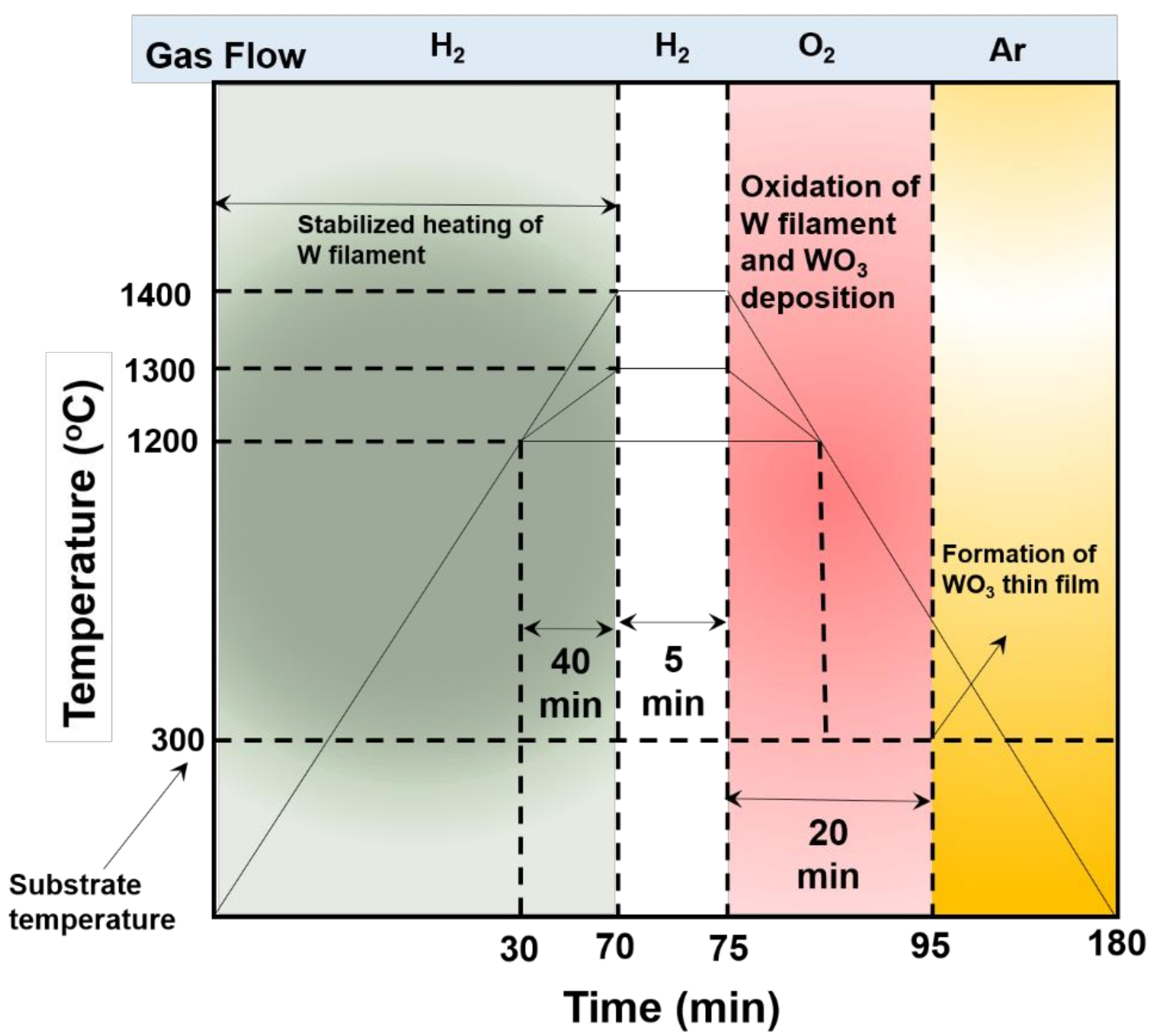
2. Materials and Methods

The WO3 NPys thin film was grown in house made HFCVD (Figure 1), comprised of a stainless-steel chamber, gas mixer, vacuum pump, gas cylinder, and clean tungsten filament as a vapor and heating source. To improve the adhesion of the thin films, silicon substrates were cleaned by acetone under ultrasonic bath, followed by rinsing in alcohol and dried in air. During experiment, a distance of 1 cm was maintained between the substrates and tungsten (W) filament in a vacuum chamber. Hydrogen (H2) and oxygen (O2) gases were injected to the process chamber via shower head gas inlet situated at the top of the electrode. Required H2 is inserted as an inert gas with flow rate of ~6.0 sccm and thereafter, filament (W) was heated between the temperature ranges from 1300 °C–1400 °C, followed by the injection of O2 at flow rate of 10 sccm for the time duration of 20 min. During an experiment, tungsten (W) filament was oxidized and created WO3 layer at the filament surface which deposited on the silicon substrates under vacuum condition. Herein throughout the experiment, the substrate temperature was kept constant at 300 °C. To evaluate the sensing performances towards ethylenediamine chemical, two-electrodes electrochemical system was applied to measure the current–voltage (I–V) characteristics (Electrometer, Keithley, 6517A, USA), in which HFCVD grown WO3 NPys thin film as working electrode and Pt foil as a counter electrode. In 10 mL of 0.1 M phosphate buffer solution (PBS, pH = 7), the sensitivity was examined, and a wide range of ethylenediamine chemical concentrations from 10 μM to 200 μM was tested. The slope of the calibrated current against ethylenediamine chemical concentration plot was divided by the active area of the sensor/electrode to estimate the sensitivity of the constructed electrode (0.15 cm2), as displayed in Equation (1).
S e n s i t i v i t y   = S l o p e   o f   c a l i b r a t e d   c u r v e A c t i v e   a r e a
The current responses were analyzed by applying a voltage range from 0–2.0 V, whilst the response time of 10 s was estimated.

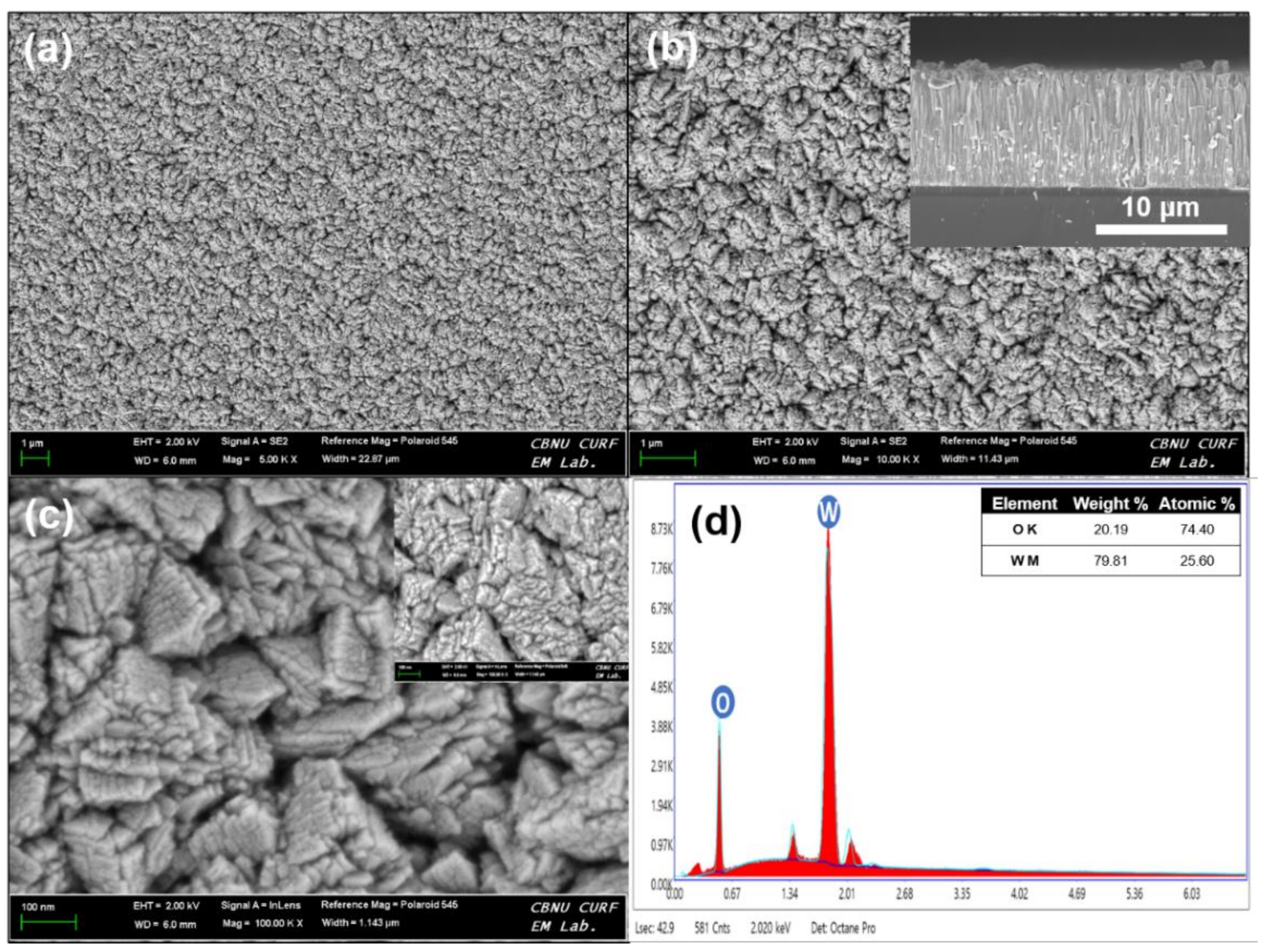
Materials Characterization
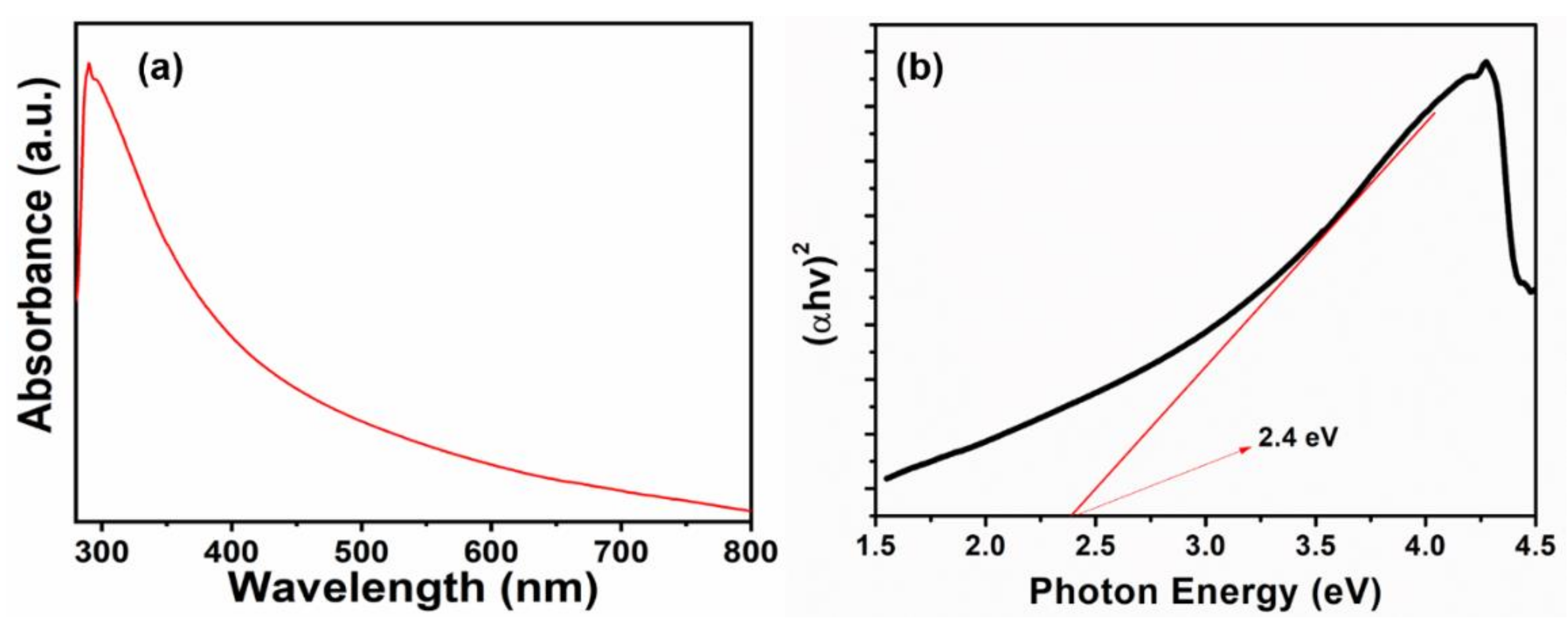
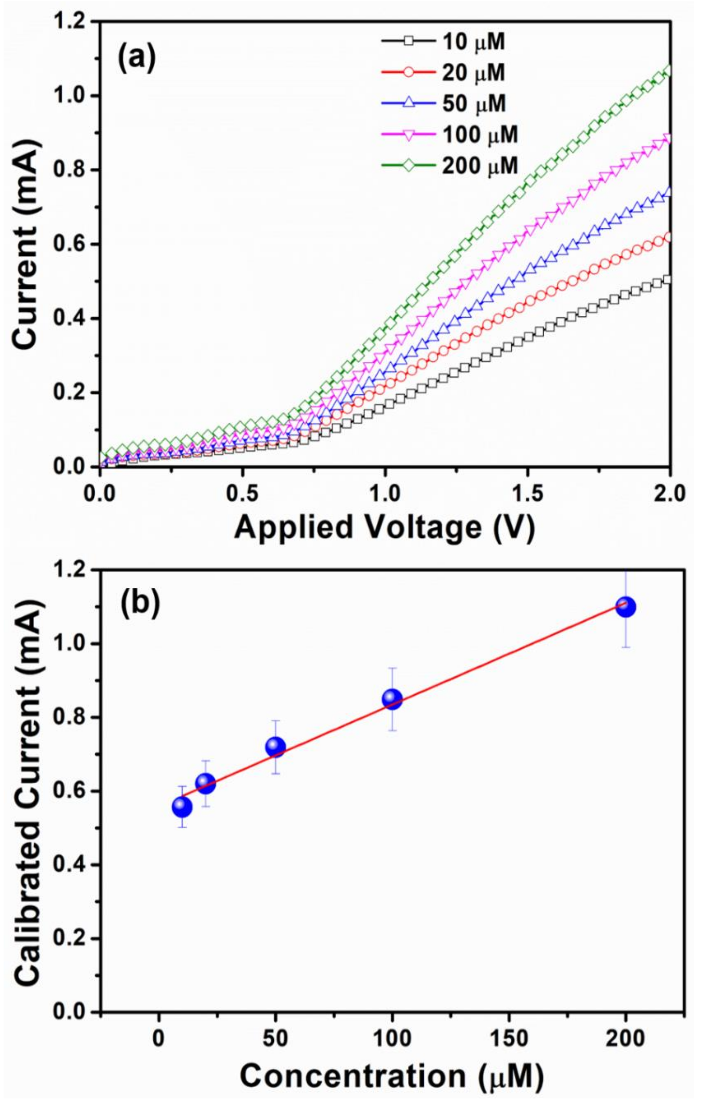
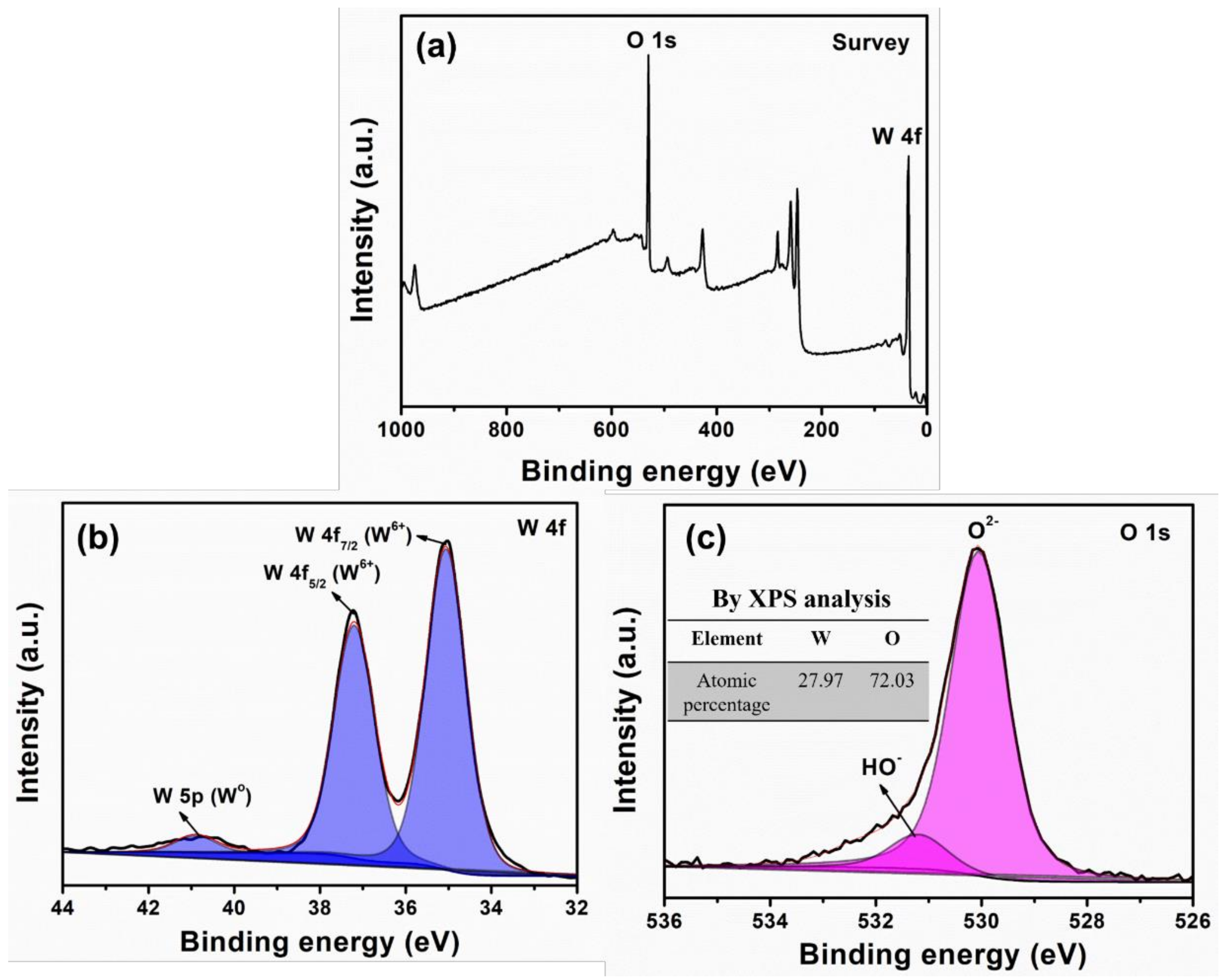
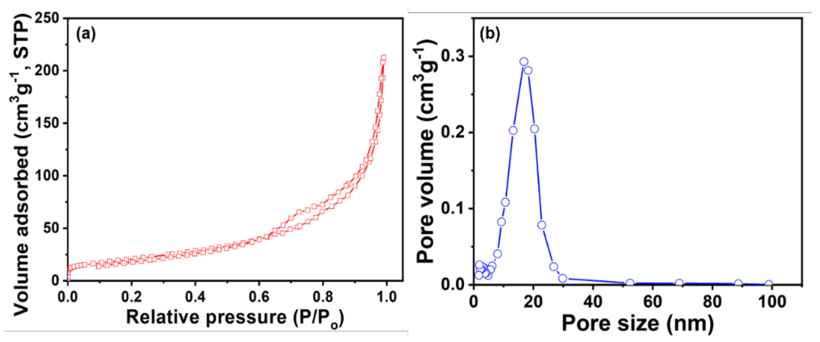
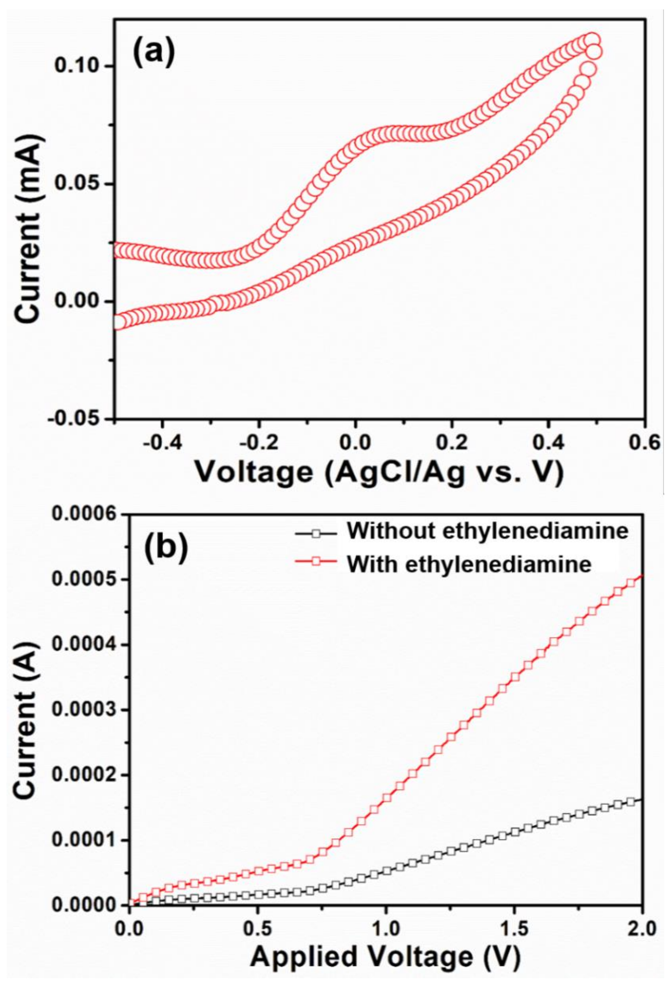
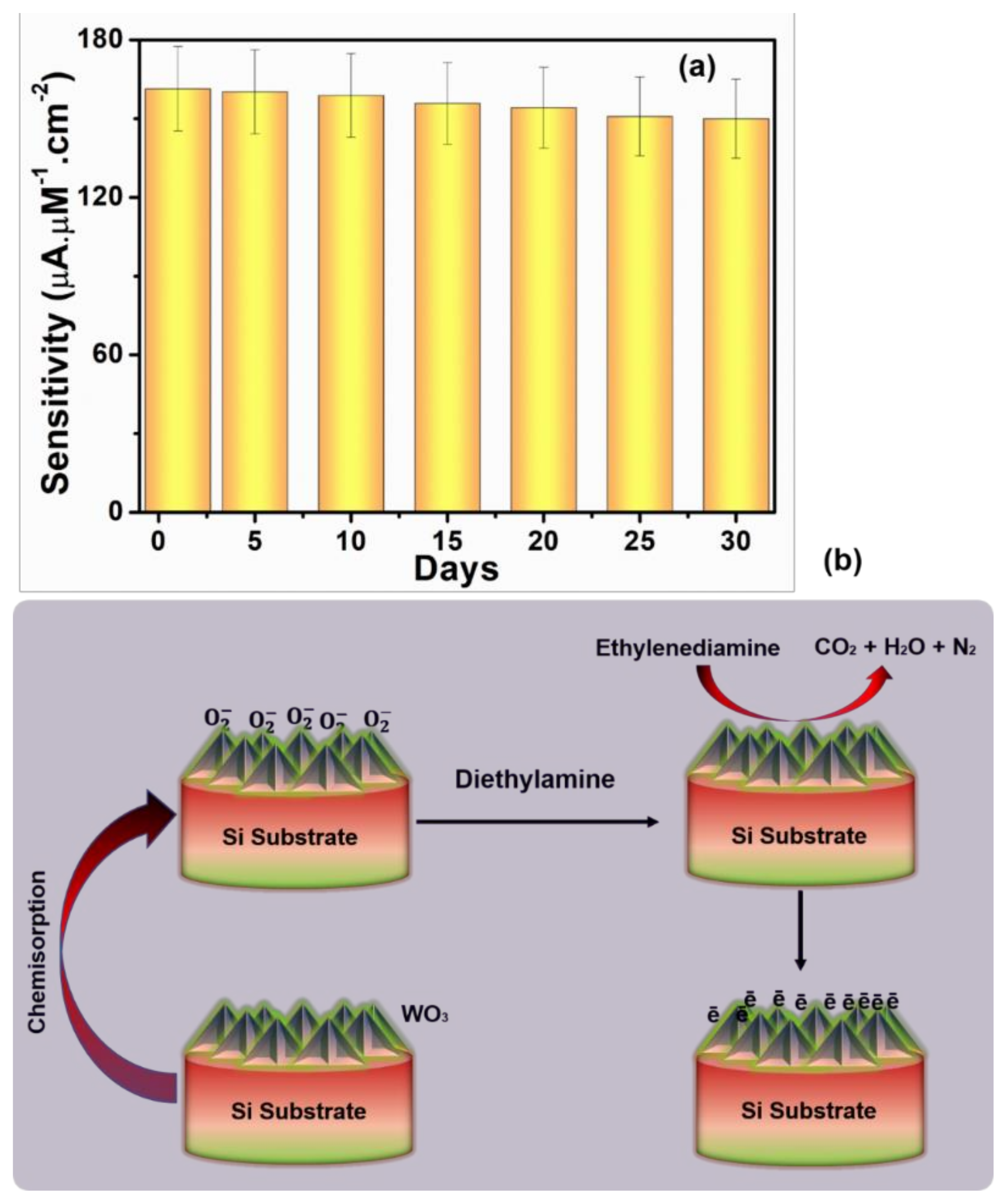
The grown WO3 thin film was morphologically examined by taking field emission scanning electron microscopic (FESEM, Hitachi S-4700, Phoenix, AZ, USA) images at low and high magnifications. The crystalline properties of grown WO3 thin film were investigated by measuring the X-ray diffraction (XRD, Rigaku, Cu-Kα, λ = 1.54178 Å, Tokyo, Japan) patterns. The structural and surface behavior of grown WO3 thin film were analyzed by Fourier transform infrared (FTIR, Nicolet, IR300, Shenzhen, China), Raman scattering (Raman micro-scope, Renishaw, Wotton-under-Edge, UK) and x-ray photoelectron spectroscopies (XPS, KRATOS AXIS-Nova, Manchester, UK). Energy dispersive spectroscopy (EDS) coupled with FESEM (Hitachi S-4700, Tokyo, Japan) system was utilized to check the elemental analysis of grown WO3 thin film. Optical behavior of grown WO3 thin film was detected by observing the ultraviolet-visible (UV–Vis, 2550 Shimadzu, Tokyo, Japan) spectroscopy. Brunauer–Emmett–Teller (BET, a Micromeritics Tristar 3000, Norcross, GA, USA) surface analyzer was used to investigate the surface properties of grown WO3 thin film.

3. Results

The morphology of HFCVD WO3 thin film for analyzing the growth is investigated by FESEM, and the presence of elements are detected by Energy Dispersive X-ray (EDAX). Figure 2a–c shows unique WO3 nano-pyramidal structures (NPys) on the surface of silicon substrate. The thin film growth appeared to begin with little grains, which then developed into pyramid-shaped grains as the deposition progresses. The surface FESEM images clearly display the evolution of the grains and the lateral sizes of the top of the grain are about ~20–25 nm. Importantly, HFCVD grown WO3 NPys thin film exhibits a good adhesion as qualitatively tested by scotch-tape method. The inset of Figure 2b reveals that the grown WO3 thin film possesses the average thickness of 12–15 μm. The EDX Figure 2d of WO3 NPys thin film clearly shows the atomic weight percentages (At. Wt.%) of ~74.40% and ~25.60%, respectively, for O and W elements. Herein, the traces of Pt are noticed, which might be due to the coating of Pt over substrate’s surface during the FESEM analysis.
The X-Ray diffraction (XRD) is used to study the structural properties of HFCVD grown WO3 NPys thin film. Figure 3 shows the XRD pattern, exhibiting the diffraction peaks and corresponding miller planes at ~23.40° (200), ~24.64° (120), ~26.94° (112), ~28.98° (022), ~33.53° (202), ~34.43° (122), ~41.78° (222), ~45.73° (004), ~48.67° (020), ~50.27° (114), ~53.81° (024), ~54.48° (204), ~56.05° (142), ~60.40° (320). The acquired XRD diffraction peaks match quite well to JCPDS card no. 83-0950 [18]. The optimal orientation (200) for the WO3 has a narrow full width at half maximum (FWHM), indicating strong crystallinity and big particle size which is also corroborated by FESEM micrographs.
The molecular architectures and chemical contaminants of produced thin films are studied by using FTIR spectroscopy. Figure 4a exhibits FTIR spectroscopy, depicting a broad transmittance edge near ~746 cm−1, which refers to O–W–O bending modes of vibrations. The occurrence of IR band at ~820 cm−1 corresponds to W–O stretching mode of hexagonal WO confirms the hexagonal structure [27]. The structural and molecular information of prepared WO3 thin film is again checked by Raman spectroscopy (Raman microscope, Renishaw, Wotton-under-Edge, UK), as shown in Figure 4b. The Raman bands at ~274.2 cm−1 and ~326.7 cm−1 are assigned to W-O-W bridging oxide vibrations and bending, respectively [28,29]. However, the Raman bands positioned at ~716.8 cm−1 and ~808.1 cm−1 correspond to O–W–O stretching modes in WO6 octahedral units of monoclinic WO3 [28,29]. The prepared WO3 thin film is totally crystalline in nature which is indicated by the features Raman bands in the ~710–818 cm−1 region [20]. Herein, strong peak at ~808 cm−1 indicates a high crystallinity of the sample [30].
To further check the quality of thin film, the absorption spectroscopy of WO3 NPys thin film in the 300–800 nm range has been investigated, as given in Figure 5a. Sharp absorption peak at ~345 nm is evident of WO3 [30]. The direct bandgap is estimated from the corresponding Tauc plot (Figure 5b), and a reasonable band gap of ~2.3 eV is estimated for grown WO3 NPy thin film which is in good line with literature value [31].
Surface and chemical nature of grown WO3 NPys thin film are determined by means of XPS. The survey profile is shown in Figure 6a, exhibiting the distinctive binding energies of W 4f and O 1s. To elaborate the XPS analysis, the high-resolution W 4f and O 1s XPS spectra have been observed to further study the fitting of W 4f and O 1s binding energies. Figure 6b displays the fitted W 4f XPS plot which poses doublet binding energies at ~35.8 and ~37.9 eV, corresponding to W 4f5/2 and W 4f7/2, respectively. Generally, WO3 materials present two binding energies in the range of ~36–38 eV, deducing the presence of W6+ in stoichiometric WO3 [20]. The prepared WO3 NPy thin film displays the doublet binding energies in the range of 36–38 eV, confirming the stoichiometric WO3 [32,33]. It is notable that the weak binding energy at ~40.9 eV represents the existence of small traces of Wo state over the WO3 thin film. In addition, Figure 6c describes the fitted O 1s XPS plot. It shows two binding energies, one of higher intensity at ~530.2 eV and the other lower intensity peak at ~532.3 eV. The higher intensity at ~530.2 eV is normally originated from the O2- of oxide, again supporting the formation of W-O bond in the prepared WO3 thin film [34,35]. Herein, the lower energy peak at ~532.3 eV is associated with OH or H2O species over the surface of thin film [36], as this contamination happens due to interaction of atmospheric moisture or the crystal water. Moreover, the atomic composition of W and O elements extracted by XPS analysis is depicted in the inset of Figure 6c-there is no inset). It is seen that W:O ratio is estimated to be 0.39 which is very close to the calculated W:O ratio of molecular formula, suggesting the nice stoichiometry in the grown WO3 thin film along with slight excess of oxygen species. Thus, with the small number of oxygenated defects, the prepared WO3 thin film is in good stoichiometric amount of W and O having typical M-O bonds.
The porous surface of HFCVD prepared WO3 NPys thin film has been investigated by the Brunauer–Emmett–Teller (BET, a Micromeritics Tristar 3000) analysis and the surface analysis results are depicted in Figure 7. A classical IV sorption isotherm accompanied with H1-type hysteresis loop is observed in the N2 adsorption-desorption isotherms of HFCVD prepared WO3 NPys thin film, as depicted in Figure 7a. It clearly discloses that the capillary condensation associated with big pore channels in WO3 pyramidal structures. Figure 7b exhibits the pore size distributions plot of HFCVD prepared WO3 NPys thin film. HFCVD prepared WO3 thin film displays the distributions of pores in the range of ~10–30 nm, representing the mesopores of WO3 pyramidal thin film. By analyzing the BJH, a reasonably good surface area of 83.74 m2/g is accounted for HFCVD prepared WO3 thin film. Thus, HFCVD prepared WO3 thin film poses reasonable surface area with mesopores, which might tend to accelerate the sensing response towards amine chemical as film surface might have a large number of active sites.
The electrochemical response of HFCVD grown WO3 NPys thin film-based sensor is studied under various concentration of ethylenediamine to investigate the electrocatalytic activity. Cyclicvoltammetry (CV) measurements (Figure 8a), are performed to elucidate the electrochemical behavior of HFCVD prepared WO3 NPys thin film based sensor in 0.1 M PBS containing 10 μM of ethylenediamine chemical. The electrochemical activities are governed by the appearance of oxidation peak in CV plot. Upon the addition of ethylenediamine chemical in PBS, an oxidation potential is noticed at ~0.11 V, exhibiting the corresponding current of ~0.07 mA. This suggests a rapid response and a good electrocatalytic activity of HFCVD grown WO3 NPys thin film based sensor towards the detection of ethylenediamine chemical at its lowest concentration. Figure 8b shows the typical current-voltage (I-V) curve of HFCVD grown WO3 NPys thin film based sensor without and with (10 μM) ethylenediamine chemical in 0.1 M PBS (pH = 7.0). Herein, the addition of ethylenediamine into PBS electrolyte has drastically increased the current whereas, a low current response is observed in pristine PBS electrolyte. This prominent current enhancement indicates a quick sensing response of HFCVD grown WO3 NPys thin film sensor towards the detection of ethylenediamine chemical.
Figure 9a depicts the sensing measurements upon the integration of different ethylenediamine concentrations from 10 μM to 200 μM in 0.1 M PBS electrolyte. It has been seen that current increases linearly with an increase in analyte concentration, favoring the formation of a large number of ions and an increase in the solution’s ionic strength. As illustrated in Figure 9b, the calibration curve of current against concentration is displayed to examine the sensitivity of the fabricated chemical sensor. Herein, the current increases linearly, w.r.t the increase in concentration of ethylenediamine chemical and thereafter, the saturation arrives. The existence of saturation confirms the unavailability of active sites for the adsorption of ethylenediamine chemical over the surface of HFCVD grown WO3 NPys thin film sensor. High and consistent sensitivity of ~161.33 μA μm−1 cm−2 with a correlation coefficient (R) of ~0.98483, a detection limit (LOD) of ~9.56 μM, and a short response time (10 s) are observed by the fabricated ethylenediamine sensor which also demonstrates a strong linearity in 10 μM–200 μM range. The observed sensitivity in this case is better than those of reported chemical sensors, as summarized in Table 1.
To examine the stability, for four weeks, the I–V properties of an HFCVD produced WO3 NPys thin film sensor were evaluated twice a day, and no significant reduction in I–V properties towards the detection of ethylenediamine was seen, as shown in Figure 10a. It clearly confirms a good stability of HFCVD grown WO3 NPys thin film based sensor. The sensing mechanism of HFCVD grown WO3 NPys thin film based sensor is related to changes in electrode resistance and conductance when it is exposed to ethylenediamine, as shown in Figure 10b. Unique porous pyramids morphology of HFCVD grown WO3 NPys thin film shows a significant amount of surface area for molecular O2 adsorption from the air [37]. With n-type WO3 semiconducting behavior, the electrons in the conduction band adhere to surface chemisorbed O2 molecules and simultaneously transform into anionic containing the oxygenated species, as shown in below reactions. As a result of the loss of conduction band electrons, an electron depletion layer (EDL) with a sufficiently high resistance and low conductance forms [38,39].
O2 (gas) ↔ O2(ads)
O2(ads) + ē (CB of WO3) ↔ O2 (ads) → O(ads)
8O + C2H4(NH2)2 ↔ 4CO2 + 4H2O + 2N2 + 4ē
Thereafter, when the ethylenediamine comes into touch with these anionic oxygenated species, it undergoes oxidation. Herein, the liberated electrons return to the conduction band, resulting in lower EDL resistance and thickness, as well as higher oxidative (anodic) peak current [40]. Thus, the growth of unique porous pyramidal morphology on WO3 thin film with excellent electrocatalytic activity result in the reliable, emulative, and high sensitivity with superb linear dynamic range to ethylenediamine chemical.
Table 1. Sensing parameters of WO3 NPys electrode based sensors compared with reported chemical sensors.
MaterialsChemicalSensitivityLODLinear DynamicRefs.
Al − ZnOPhenyl-hydrazine1.143 μA·mM−1·cm−21.215 μM10 μM–50 mM[41]
CuO − ZnONH4OH1.549 μA·mM−1·cm−28.9 μM77 μM–7.7 M[42]
Fe,Ni − ZnOHexahydropyridine62.28 μA·μM−1·cm−279 μM0.1 μM–1 mM[43]
ZnO nanopencilsAmmonia26.58 μA·cm−2·μM−15 nM-[44]
ZnO nanonailsHydrazine8.56 μA·cm−2·μM−10.2 μM-[45]
WO3 NPysEthylenediamine161.33μA·μM−1·cm−29.56 μM10–200 μMThis work

4. Conclusions

WO3 thin films of highly dense pyramidal nanostructures are successfully synthesized at low temperature of ~300 °C by HFCVD process. Highly crystalline and large grain size WO3 NPys thin films are utilized for the fabrication of ethylenediamine chemical sensor. WO3 NPys thin film sensor readily detects ethylenediamine chemical at low concentration and displays a high sensitivity of ~161.33 μA μm−1 cm−2 with a correlation coefficient (R) of ~0.98483, a LOD of ~9.56 μM, and a short response time (10 s). The fabricated HFCVD prepared WO3 NPys thin film based sensor is promising and could be used to evaluate other harmful compounds in the future.

Author Contributions

Conceptualization, M.I., M.S.A. and S.A.; methodology, M.I.; software, M.I., M.S.A., D.-H.K. and E.-B.K.; validation, M.I., M.S.A. and E.-B.K.; formal analysis, M.I. and E.-B.K.; investigation, M.I.; resources, M.I.; data curation, M.I., M.S.A. and S.A.; writing—original draft preparation, M.I. and E.-B.K.; writing—review and editing, M.S.A. and S.A.; supervision, S.A.; project administration, M.S.A. and D.-H.K.; funding acquisition, M.S.A., D.-H.K. and E.-B.K. All authors have read and agreed to the published version of the manuscript.

Funding

This research was funded by the NRF granted funded by MSIT (No. 2019R1F1063999). E.B. Kim acknowledges the research grant from NRF Korea (Project No.: 2020R1A6A3A13070611). This paper is also supported by research funds of Jeonbuk National University in 2020.

Institutional Review Board Statement

Not applicable.

Informed Consent Statement

Not applicable.

Data Availability Statement

Not applicable.

Acknowledgments

Authors would like to acknowledge the support from the National Research Foundation of Korea (NRF) grant funded by the Korea government (MSIT) (No. 2019R1F1063999). E.B. Kim acknowledges the research grant from NRF Korea (Project No.: 2020R1A6A3A13070611). This paper was acknowledged the selection of research-oriented Professor of Jeonbuk National University in 2021.

Conflicts of Interest

The authors declare no conflict of interest.

References

  1. Jitan, S.A.; Palmisano, G.; Garlisi, C. Synthesis and surface modification of TiO2-based photocatalysts for the conversion of CO2. Catalysts 2020, 10, 227. [Google Scholar] [CrossRef] [Green Version]
  2. Sun, L.; Shi, Z.; Liang, L.; Wei, S.; Wang, H.; Dastan, D.; Sun, K.; Fan, R. Layer-structured BaTiO3/P(VDF–HFP) composites with concurrently improved dielectric permittivity and breakdown strength toward capacitive energy-storage applications. J. Mater. Chem. C 2020, 8, 10257–10265. [Google Scholar] [CrossRef]
  3. Yang, J.; Zhu, X.; Wang, H.; Wang, X.; Hao, C.; Fan, R.; Dastan, D.; Shi, Z. Achieving excellent dielectric performance in polymer composites with ultralow filler loadings via constructing hollow-structured filler frameworks. Compos. Part A 2020, 131, 105814. [Google Scholar] [CrossRef]
  4. Yin, X.T.; Li, J.; Dastan, D.; Zhou, W.D.; Garmestani, H.; Alamgir, F.M. Ultra-high selectivity of H2 over CO with A P-N nanojunction based gas sensors and its mechanism. Sens. Actuator B Chem. 2020, 319, 128330. [Google Scholar] [CrossRef]
  5. Granqvist, C.G. Electrochromic tungsten oxide films: Review of progress 1993–1998. Sol. Energy Mater. Sol. Cells 2000, 60, 201–262. [Google Scholar] [CrossRef]
  6. White, C.M.; Gillaspie, D.T.; Whitney, E.; Lee, S.H.; Dillon, A.C. Flexible electrochromic devices based on crystalline WO3 nanostructures produced with hot-wire chemical vapor deposition. Thin Solid Films 2009, 517, 3596–3599. [Google Scholar] [CrossRef]
  7. Yin, X.T.; Lv, P.; Lia, J.; Jafari, A.; Wu, F.Y.; Wang, Q.; Dastan, D.; Shi, Z.; Yue, S.; Garmestani, H. Nanostructured tungsten trioxide prepared at various growth temperatures for sensing applications. J. Alloys Comp. 2020, 825, 154105. [Google Scholar] [CrossRef]
  8. Franke, E.B.; Trimble, C.L.; Hale, J.S.; Schubert, M.; Woollam, J.A. Infrared switching electrochromic devices based on tungsten oxide. J. Appl. Phys. 2000, 88, 5777–5784. [Google Scholar] [CrossRef] [Green Version]
  9. Trimble, C.; DeVries, M.; Hale, J.S.; Thompson, D.W.; Tiwald, T.E.; Woollam, J.A. Infrared emittance modulation devices using electrochromic crystalline tungsten oxide, polymer conductor, and nickel oxide. Thin Solid Films 1999, 355–356, 26–34. [Google Scholar] [CrossRef]
  10. Bussjager, R.; Chaiken, J.; Getbehead, M.; Grucza, D.; Hinkel, D.; McEwen, T.; Osman, J.; Voss, E. Using tungsten oxide based thin films for optical memory, and the effects of using IR combined with blue/blue-green wavelengths. Jpn. J. Appl. Phys. 2000, 39, 789–796. [Google Scholar] [CrossRef]
  11. Turyan, I.; Krasovec, U.O.; Orel, B.; Saraidorov, T.; Reisfeld, R.; Mandler, D. “Writing–reading–erasing” on tungsten oxide films using the scanning electrochemical microscope. Adv. Mater. 2000, 12, 330–333. [Google Scholar] [CrossRef]
  12. Zhang, W.; Zhu, X.; Liang, L.; Yin, P.; Xie, P.; Dastan, D.; Sun, K.; Fan, R.; Shi, Z. Significantly enhanced dielectric permittivity and low loss in epoxy composites incorporating 3d W-WO3/BaTiO3 foams. J. Mat. Sci. 2021, 56, 4254–4265. [Google Scholar] [CrossRef]
  13. Gillet, M.; Aguir, K.; Bendahan, M.; Mennini, P. Grain size effect in sputtered tungsten trioxide thin films on the sensitivity to ozone. Thin Solid Films 2005, 484, 358–363. [Google Scholar] [CrossRef]
  14. Fukuda, H.; Zohnishi, R.; Nomura, S. Highly sensitive metal-insulator-semiconductor field-effect transistor sensors for detecting carbon monoxide gas using porous platinum and tungsten oxide thin films. Jpn. J. Appl. Phys. 2001, 40, 2782–2786. [Google Scholar] [CrossRef]
  15. Fang, L.; Baik, S.J.; Lim, K.S.; Yoo, S.H.; Seo, M.S.; Kang, S.J.; Seo, J.W. Tungsten oxide as a buffer layer inserted at the SnO2/P-A-Sic interface of pin-type amorphous silicon based solar cells. Appl. Phys. Lett. 2010, 96, 193501. [Google Scholar] [CrossRef]
  16. Saito, Y.; Uchida, S.; Kubo, T.; Segawa, H. Surface-oxidized tungsten for energy-storable dye-sensitized solar cells. Thin Solid Films 2010, 518, 3033–3036. [Google Scholar] [CrossRef]
  17. Mendoza, F.; Limbu, T.B.; Weiner, B.R.; Morell, G. Hot filament chemical vapor deposition: Enabling the scalable synthesis of bilayer graphene and other carbon materials. ACS Appl. Nano Mater. 2018, 4, 1502–1512. [Google Scholar] [CrossRef] [Green Version]
  18. Godbole, R.; Ameen, S.; Nakate, U.T.; Akhtar, M.S.; Shin, H.S. Low temperature HFCVD synthesis of tungsten oxide thin film for high response hydrogen gas sensor application. Mater. Lett. 2019, 254, 398–401. [Google Scholar] [CrossRef]
  19. Tan, G.L.; Tang, D.; Dastan, D.; Jafari, A.; Silva, J.P.B.; Yin, X.T. Effect of heat treatment on electrical and surface properties of tungsten oxide thin films grown by HFCVD technique. Mater. Sci. Semicon. Process. 2021, 122, 105506. [Google Scholar] [CrossRef]
  20. Jacob, S.P.C. The influence of substrate temperature variation on tungsten oxide thin film growth in an HFCVD system. Appl. Surf. Sci. 2007, 253, 3317–3325. [Google Scholar]
  21. Jafari, A.; Ghoranneviss, M.; Elahi, A.S. HFCVD application for growth of monoclinic tungsten trioxide crystal nano-walls. J. Inorg. Organomet. Polym. Mater. 2016, 26, 254–258. [Google Scholar] [CrossRef]
  22. Feng, P.X.; Wang, X.P.; Zhang, H.X.; Yang, B.Q.; Wang, Z.B.; Berríos, A.G. Study of the structural evolutions of crystalline tungsten oxide films prepared using hot-filament CVD. J. Phys. D Appl. Phys. 2007, 40, 5239. [Google Scholar] [CrossRef]
  23. Ethylenediamine. Available online: https://en.wikipedia.org/wiki/Ethylenediamine (accessed on 20 August 2021).
  24. Ameen, S.; Akhtar, M.S.; Shin, H.S. Highly sensitive hydrazine chemical sensor fabricated by modified electrode of vertically aligned zinc oxide nanorods. Talanta 2012, 100, 377–383. [Google Scholar] [CrossRef] [PubMed]
  25. Singh, K.; Mehta, S.K. Utilization of ZnO nanoflowers as efficient electrochemical catalyst for the oxidation of hydrazine. Sens. Lett. 2015, 13, 1002–1006. [Google Scholar] [CrossRef]
  26. Ibrahim, A.A.; Dar, G.N.; Zaidi, S.A.; Umar, A.; Abaker, M.; Bouzid, H.; Baskoutas, S. Growth and properties of Ag-doped ZnO nanoflowers for highly sensitive phenyl hydrazine chemical sensor application. Talanta 2012, 93, 257–263. [Google Scholar] [CrossRef]
  27. Tan, G.-L.; Tang, D.; Dastan, D.; Jafari, A.; Shi, Z.; Chu, Q.Q.; Silva, J.P.B.; Yin, X.T. Structures, morphological control, and antibacterial performance of tungsten oxide thin films. Ceram. Int. 2021, 47, 17153–17160. [Google Scholar] [CrossRef]
  28. Anderson, A. Raman study of ceramic tungsten trioxide at low temperatures. Spectrosc. Lett. 1976, 9, 809–819. [Google Scholar] [CrossRef]
  29. Souza-Filho, A.G.; Freire, V.N.; Sasaki, J.M.; Mendes, F.J.; Julio, J.F.; Gomes, U.U. Coexistence of triclinic and monoclinic phases in WO3 ceramics. J. Raman Spectrosc. 2000, 31, 451–454. [Google Scholar] [CrossRef]
  30. Chatterjee, P.; Chakraborty, A.K. Band-gap engineering of tungsten oxide nanoplates by cobalt ferrite Co-catalyst for solar water oxidation. Opt. Mater. 2021, 111, 110610. [Google Scholar] [CrossRef]
  31. Asres, G.A.; Dombovari, A.; Sipola, T.; Puskás, R.; Kukovecz, A.; Kónya, Z.; Popov, A.; Lin, J.F.; Lorite, G.S.; Mohl, M.; et al. A novel WS2 nanowire-nanoflake hybrid material synthesized from WO3 nanowires in sulfur vapor. Sci. Rep. 2016, 6, 25610. [Google Scholar] [CrossRef] [Green Version]
  32. Lozzi, L.; Ottaviano, L.; Passacantando, M.; Santucci, S.; Cantalini, C. The influence of air and vacuum thermal treatments on the NO2 gas sensitivity of WO3 thin films prepared by thermal evaporation. Thin Solid Films 2001, 391, 224–228. [Google Scholar] [CrossRef]
  33. Leftheriotis, G.; Papaefthimiou, S.; Yianoulis, P.; Siokou, A. Effect of the tungsten oxidation states in the thermal coloration and bleaching of amorphous WO3 films. Thin Solid Films 2001, 384, 298–306. [Google Scholar] [CrossRef]
  34. Soto, G.; De La Cruz, W.; Díaz, J.A.; Machorro, R.; Castillón, F.F.; Farías, M.H. Characterization of tungsten oxide films produced by reactive pulsed laser deposition. Appl. Surf. Sci. 2003, 218, 281–289. [Google Scholar] [CrossRef]
  35. Joshi, N.; da Silva, L.F.; Jadhav, H.S.; Shimizu, F.M.; Suman, P.H.; M’Peko, J.C.; Orlandie, M.O.; Seo, J.G.; Mastelaro, V.R.; Oliveira, O.N., Jr. Yolk-shelled ZnCo2O4 microspheres: Surface properties and gas sensing application. Sens. Act. B Chem. 2018, 257, 906–915. [Google Scholar] [CrossRef] [Green Version]
  36. Li, N.; Fan, Y.; Shi, Y.; Xiang, Q.; Wang, X.; Xu, J. A low temperature formaldehyde gas sensor based on hierarchical SnO/SnO2 nano-flowers assembled from ultrathin nanosheets: Synthesis, sensing performance and mechanism. Sen. Act. B Chem. 2019, 294, 106–115. [Google Scholar] [CrossRef]
  37. Zhang, Y.; Huang, B.; Ye, J.; Ye, J. A sensitive and selective amperometric hydrazine sensor based on palladium nanoparticles loaded on cobalt-wrapped nitrogen-doped carbon nanotubes. J. Electroanal. Chem. 2017, 801, 215–223. [Google Scholar] [CrossRef]
  38. Li, Y.; Wang, S.; Hao, P.; Tian, J.; Cui, H.; Wang, X. Soft-templated formation of double-shelled ZnO hollow microspheres for acetone gas sensing at low concentration/near room temperature. Sens. Actuators B Chem. 2018, 273, 751–759. [Google Scholar] [CrossRef]
  39. Wang, P.; Dong, T.; Jia, C.; Yang, P. Ultraselective acetone-gas sensor based ZnO flowers functionalized by au nanoparticle loading on certain facet. Sens. Actuat. B Chem. 2019, 288, 1–11. [Google Scholar] [CrossRef]
  40. Zhang, H.-J.; Liu, L.-Z.; Zhang, X.-R.; Zhang, S.; Meng, F.-N. Microwave-assisted solvothermal synthesis of shape-controlled CoFe2O4 nanoparticles for acetone sensor. J. Alloys Compd. 2019, 788, 1103–1112. [Google Scholar] [CrossRef]
  41. Rahman, M.M.; Bahadar Khan, S.; Jamal, A.; Faisal, M.; Abdullah, M. Asiri, fabrication of phenyl-hydrazine chemical sensor based on Al-doped ZnO nanoparticles. Sens. Trans. J. 2011, 134, 32–44. [Google Scholar]
  42. Rahman, M.M.; Jamal, A.; Khan, S.B.; Faisal, M. CuO codoped ZnO based nanostructured materials for sensitive chemical sensor applications. ACS Appl. Mater. Interfaces 2011, 3, 1346–1351. [Google Scholar] [CrossRef] [PubMed]
  43. Kim, E.B.; Ameen, S.; Akhtar, M.S.; Shin, H.S. Iron-nickel co-doped ZnO nanoparticles as scaffold for field effect transistor sensor: Application in electrochemical detection of hexahydropyridine chemical. Sens. Actuators B Chem. 2018, 275, 422–431. [Google Scholar] [CrossRef]
  44. Dar, G.N.; Umar, A.; Zaidi, S.A.; Baskoutas, S.; Hwang, S.W.; Abaker, M.; Al-Hajry, A.; Al-Sayari, S.A. Ultra-high sensitive ammonia chemical sensor based on ZnO nanopencils. Talanta 2012, 89, 155–161. [Google Scholar] [CrossRef] [PubMed]
  45. Umar, A.; Rahman, M.M.; Kim, S.H.; Hahn, Y.B. Zinc oxide nanonail based chemical sensor for hydrazine detection. Chem. Commun. 2008, 2, 166–168. [Google Scholar] [CrossRef]
Figure 1. A representation of HFCVD process for the growth of WO3 NPys thin film.
Chemosensors 09 00257 g001
Figure 2. FESEM images (ac) and EDAX spectrum (d) of HFCVD deposited WO3 NPys thin film. Inset shows the cross-section of WO3 NPys thin film.
Chemosensors 09 00257 g002
Figure 3. XRD patterns of HFCVD grown WO3 NPys thin film with corresponding JCPDS.
Chemosensors 09 00257 g003
Figure 4. (a) FTIR spectroscopy and (b) Raman spectroscopy of HFCVD grown WO3 NPys thin film.
Chemosensors 09 00257 g004
Figure 5. (a) UV-Vis spectrum and (b) its corresponding tauc plot of HFCVD grown WO3 NPys thin film.
Chemosensors 09 00257 g005
Figure 6. (a) Survey, (b) W 4f and (c) O 1s XPs of HFCVD grown WO3 NPys thin film. Inset shows the element composition analysis by XPS measurement.
Chemosensors 09 00257 g006
Figure 7. (a) N2 adsorption–desorption isotherms and (b) pore size distributions of HFCVD prepared WO3 NPys thin film.
Chemosensors 09 00257 g007
Figure 8. (a) Cyclicvoltametry plot with ethylenediamine chemical (10 μM) in 0.1 M PBS of HFCVD grown WO3 NPys thin film and (b) I-V curves of HFCVD grown WO3 NPys thin film based chemical sensor without and with ethylenediamine chemical (10 μM) in 0.1 M PBS.
Chemosensors 09 00257 g008
Figure 9. (a) Typical I-V curves with varying ethylenediamine concentrations from 10 μM to 200 μM and (b) calibrated current versus concentration of ethylenediamine chemical of HFCVD grown WO3 NPys thin film based chemical sensor.
Chemosensors 09 00257 g009
Figure 10. (a) Stability test through I-V measurements in the presence of 10 μM ethylenediamine chemical in 0.1 M PBS and (b) schematic mechanism of the fabricated ethylenediamine chemical sensor based on HFCVD grown WO3 NPys thin film.
Chemosensors 09 00257 g010
Publisher’s Note: MDPI stays neutral with regard to jurisdictional claims in published maps and institutional affiliations.

