Abstract
This paper presents the design and realization of a compact printed ultra-wideband (UWB) antenna with notching characteristics for compact devices using a genetic algorithm. The antenna is capable of mitigating an adjacent sub-band ranging from 3.75 to 4.875 GHz, mainly used by many applications and standards such as WiMAX, WLAN and sub-6-GHz. The notch band functionality is achieved by etching out two symmetrical slots from the pentagonal radiating element. The simulation and measured results demonstrate that the proposed antenna overperformed compared with state-of-the-art antennas in terms of compactness with an overall size of . Moreover, the proposed design shows a large bandwidth in the UWB region with a fractional bandwidth of 180% with respect to the center frequency of 5.25 GHz. The antenna also presents omnidirectional radiations all over the operation band and a good return loss performance.
1. Introduction
Recently, considerable interest has been devoted to ultra-wideband (UWB) technology due to its unprecedented impact on communication systems. It has demonstrated its relevance for several applications including wearable devices, tracking and positioning, radar and medical applications; more precisely, in cancer detection. It is also used in radio frequency identification (RFID), security systems, distance measuring systems and many other systems [1]. The diversity of this type of technology is because of its enormous available bandwidth starting from 3.1 to 10.6 GHz, i.e., 110% of the fractional bandwidth. The UWB system presents other exciting features. Several of its key benefits are related to its low complexity and cost due to the baseband nature of the signal transmission. UWB technology possesses greater merit over other technologies because of its ability to attenuate lobes in sparse antenna array systems and its resistance to interference and intense multipath propagation. All these advantages and many more make the UWB technique very attractive for short-range communications [2].
The antenna is the most critical component of UWB communication systems. Therefore, in order not to detract from its overall performance, a properly designed antenna should be used. The antenna placed in the front-ends of the communication system should respect the fundamental restrictions imposed by physics and practical consideration limits. The UWB antenna must be characterized by a high level of conformity, a low manufacturing cost and should be easily housed into miniaturized circuits. Moreover, it should exhibit a stable response regarding impedance matching, bandwidth, gain and radiation characteristics in the operating band to be acceptable for mass production [3].
Many studies have been carried out on various antenna types to achieve a wide bandwidth along with high-performance parameters. The commonly employed techniques are the design of various Vivaldi antennas, spiral antennas, log-periodic antennas and disk-cone antennas [4,5,6,7]. However, these types of antennas suffer from a bigger dimension, which limits their use for compact size devices. Another commonly used technique to design a high gain and wideband antenna is to manipulate the near-field by loading the antenna with a meta-surface, as explained in [8,9,10]. Alternatively, the meta-surface can be used to the radiation characteristics of the antenna [11]. In both cases, the loading of the meta-surface significantly increases the size and height of the overall antenna, which results in a big device size. Therefore, these types of antennas cannot be used for small physical devices. Recently, several researchers utilized multiple rings arranged concentrically around the antenna to design wideband antennas with monopole-like radiation characteristics [12,13]. These antennas can be used for on-body applications due to the fully backed ground plane. However, their larger physical dimension limits their use for applications where size is a constraint.
Printed antennas have been widely studied and proven to be highly relevant for UWB applications. The overperformance of the latter is due to their small and low profile, their robustness and their ease of integration in UWB communication systems [14,15,16]. In [14], a printed multiband monopole antenna for WiMAX/WLAN applications with relative bandwidths of 64% and 4.08% is discussed. However, the antenna gain at the operating frequency was low, which affected the transmission distance. In [15], a good UWB candidate consisting of a circular sickle-shaped polarized antenna with a fractional bandwidth (FBW) of 126.85% is presented. However, the return loss response should be optimized further all over the operating band. In [16], a UWB printed antenna with a fork-shaped stub is proposed. The proposed antenna in this paper indicated a 17.9% wider bandwidth compared with its parent design. However, the level of complexity of the resulting antenna was higher, which significantly increases the fabrication errors for mass production.
Other interesting UWB printed antennas with a significant available bandwidth while exhibiting notch band characteristics have been discussed [17,18,19,20]. In [17], the authors present a printed antenna loaded with a split-ring with dual-band and wideband notch characteristics. The multimode behavior in this work was achieved by varying the dimensions of the SRR without having to adjust the radiating patch or the ground plane. However, this antenna presented a major drawback of having a bulky size of . In the same context, a UWB printed antenna with a wide rectangular notched band using electromagnetic bandgap structures is discussed in [18], characterized by a high efficiency and good antenna performance. However, it has the disadvantages of a larger size , making it inconvenient for miniaturized devices. An interesting printed UWB antenna with a compact size is discussed in [19]. The proposed antenna consisted of a miniaturized cylindrical UWB antenna with a modified partial ground plane. The simulation and measured results showed notch band characteristics along with a good radiation pattern. However, its geometry remained complex due to the integration of capacitors and slot resonators.
After a thorough investigation of the related papers, we deduced that a significant amount of research has been carried out to design a suitable antenna for UWB technology. The designed antenna should cover the UWB range, present a compact size and retain a good performance in terms of matching, VSWR, gain and all the radiation characteristics. Moreover, a UWB antenna with notch band characteristics is highly desirable for future handheld devices. The notch band characteristic allows the antenna to mitigate coexisting sub-bands in the UWB region to reduce interference without introducing complex circuits into the antenna design [20]. Therefore, this paper presents a low-profile pentagon compact printed monopole antenna with a notch band characteristic. The pentagonal shape choice was because this radiating element shape exhibits a larger bandwidth than conventional shapes [21,22]. Moreover, we introduced stubs to achieve a larger bandwidth in the UWB region with an FBW of 179% regarding the center frequency of 5.25 GHz. Thus, the proposed design is characterized by a low level of complexity and can easily be accommodated in future handheld devices. The resulting antenna can mitigate a sub-band ranging from 3.75 to 4.87 GHz, mainly used by several standards such as WLAN.
The rest of the paper is organized as follows: Section 2 illustrates the design methodology of the proposed antenna. Section 3 presents a comparison between the simulated and measured results and compares the state-of-the-art antennas at the same frequency and type of application. A conclusion is presented in Section 4 of the paper.
2. Antenna Design and Methodology
2.1. Antenna Design
The proposed antenna discussed in this paper is illustrated in Figure 1 and its associated parameters are shown in Table 1. The substrate of 0.508 mm thickness was made using Rogers RO4350 characterized by a relative permittivity of 3.66 and a loss tangent of 0.004. The radiating patch had a polygon shape and was designed using copper according to a standard thickness (0.035 mm) with an effective length of at the center frequency of 5.2 GHz. The number of corners of the polygonal patch and its radius were optimized to obtain the maximum bandwidth. A parametric study showed that the pentagon shape obtained the best results. It was fed using a coplanar waveguide line (CPW) to transfer the maximum power to the antenna and because of its advantage of obtaining wider bandwidths [23]. The antenna was simulated in CST Microwave Studio, which is a commercial finite element solver for electromagnetic structures. A genetic algorithm was used for optimization. Subsequently, a prototype was fabricated to compare the simulation and the measured results in order to validate the performance of the proposed antenna.
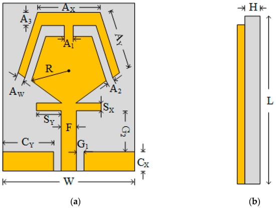
Figure 1.
Configuration of the proposed antenna: (a) Front view and (b) side view.

Table 1.
Optimized parameters of the antenna.
The shape of the radiating element was inspired initially from a conventional monopole antenna where its length was calculated using the following equation [24]:
where refers to the velocity of light in the free space, represents the central frequency and is the effective dielectric constant of the used dielectric in the antenna design. The equation of calculating an approximate value of is given by:
where and H represent the width of the radiator and the dielectric thickness, respectively.
The classic rectangular radiating patch was transformed into a pentagonal shape due to the large bandwidth that this antenna could achieve. The primary antenna also featured a horizontal stub below the radiating element for further bandwidth enhancement, as shown in Figure 2. According to the literature, introducing stubs into the radiating part increases the current distribution path and the antenna’s electrical length, as shown in Figure 3 As a result, the characteristics of the antenna, particularly the bandwidth, are improved [24]. This phenomenon can be verified by analyzing Figure 4. As can be seen, adding the stub increased the antenna matching as well as the operational bandwidth of the antenna. The primary antenna without a stub exhibited a bandwidth ranging from 3.75 to 7.56 GHz whereas it presented a bandwidth ranging from 3.75 to 14.25 GHz after introducing the stub; i.e., 6.69 GHz of extra bandwidth. Introducing the stub allowed the current to flow in several paths, which increases the number of resonances of the antenna [25].
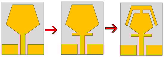
Figure 2.
The design evolution of the proposed antenna.
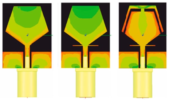
Figure 3.
The current distribution of the antenna at various design steps.
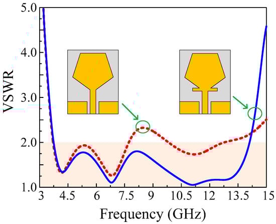
Figure 4.
VSWR response of the radiating element with and without the stub.
2.2. Design of a Notch Band Antenna
Although UWB antennas are highly desirable for future devices due to their considerable bandwidth, this type of antenna presents a significant challenge. Due to this large bandwidth, the antenna may be prone to interference from adjacent systems that reside in the UWB region. Among the most common sub-bands that we sought to mitigate were wireless local area networks (WLANs) (3.35 GHz (3.3∓3.4 GHz), 3.5 GHz (3.4 to 3.6 GHz), 3.7 GHz (3.6 to 3.8 GHz) and 5.7 GHz (5.725 to 5.85 GHz)), WiMAX (3.4 and 5.8 GHz), the first segment of the sub-6-GHz band (3.4–3.7 GHz) of the 5G communication network and many other communication systems. Filters are commonly used to attenuate the adjacent bands and therefore enhance the communication quality. However, this technique presents the drawback of insertion losses as well as the increase in volume and complexity of the resulting antenna [26]. Thus, the researchers mainly focused on more practical techniques to avoid potential interference from existing adjacent bands. These band rejection approaches included etching out the split-ring (SRR) and complementary split-ring resonators (CSRR), which exhibit a stop-band when excited by a time-varying axial electric field as illustrated in [27,28]. Other techniques have been considered such as introducing slots on the radiating element [26,29] and DGS in the ground plane [19,30] or using parasitic elements [31] or by combining multiple techniques [32]. In this paper, we considered notching the unwanted bands using slots introduced in the radiating patch. This approach is the most frequently used to reduce interference between bands for the promising results it achieves while maintaining a compact geometry with a simple design.
After designing the UWB antenna covering the entire UWB region, we moved on to etching two symmetrical slots from the radiating element to attenuate the sub-band ranging from 3.75–4.875 GHz, which is mainly used for WLAN, WiMAX, 5G and many other communication technologies. The most critical parameters in the slotted notched band antenna design are the length, position and shape of the slot. Therefore, a thorough parametric study was carried out to determine the optimal position to place the slot to achieve higher VSWR values to attenuate the desired bands. For the said purpose, slots of various shapes were utilized and it was observed during the analysis that the proposed slot offered a higher VSWR compared with other shapes. The length of the slot was determined by the following equation [23]:
where presents the central frequency of the notch, c is the velocity of light in the free space and stands for the effective dielectric constant calculated by the following formula:
As for the shape of the slot, our choice was based on the slot shapes used in [23], then transformed to meet the specifications of our antenna by the bias of a parametric study. Figure 5 presents a comparison of the VSWR results of the proposed antenna before and after adding two symmetrical slots into the radiating element. As can be observed, the antenna before the introduction of the slots covered the entire UWB region from 3.75 to 14.25 GHz.
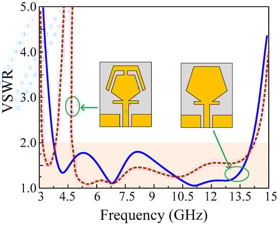
Figure 5.
VSWR of the radiating element before and after the slots.
However, after introducing the notches, the antenna rejected the band spectrum from 3.75 to 4.9 GHz, with a peak VSWR of 42 at 4.5 GHz. The effective inductance and capacitance of the microstrip line varied by adding the capacitance, inductance and resistance of the introduced slots. As the area of the slot is directly proportional to its effective inductance, any increase will generate effective inductances, which results in changing the cut-off frequency [33].
2.3. Numerical Analysis
Figure 6 depicts the equivalent circuit of the conventional as well as the resultant antenna. Generally, monopole antennas are represented by the first canonical form, which is suitable for modeling electric antennas. This model acts as an open circuit to the DC input signal and is designed by combining the RLC components in a series. Each group of RLC components results in an independent frequency so that all of the resulting frequencies overlap to form the UWB antenna [34]. We introduced a stub, which was a court-circuited line of length S connected in a shunt on the mainline at a distance d from the load, to enhance antenna matching. Eventually, we modeled the right and left slots by the RLC components. The following formula gives the corresponding frequency of the slots:
where and are the sum of the capacitances and inductances generated by the slots, respectively.
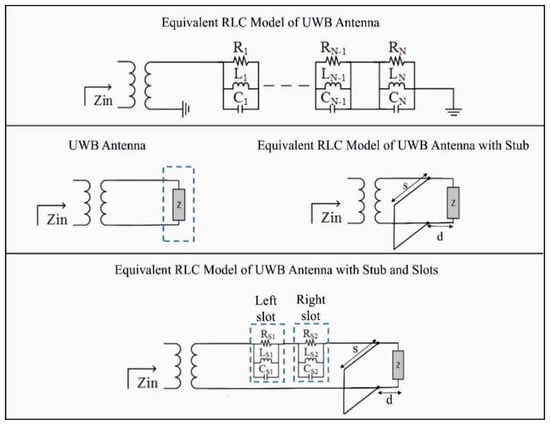
Figure 6.
Equivalent circuit model of the proposed antenna.
Theoretically speaking, the slots introduced affect the distribution of the current, which results in a lengthening of the current path. In fact, the series inductance was given by the length of the current path whereas the series capacitance was given by accumulated charges in the etched spaces. In general, this behavior was modeled by the parallel equivalent lumped components RSi, LSI and CSi, as illustrated in Figure 5. The series combination of the lumped effect of the slots was then added to the inductive patch and capacitive ground plane. Both the inductive and capacitive effects of all mentioned components contributed to the input impedance of the antenna.
2.4. Design Methodology and Optimization
Figure 7 illustrates the flow chart of the proposed antenna design. In the first instance, a rectangular monopole antenna was designed according to the mathematical equations provided by the antenna literature [35]. The physical dimensions of the conventional antenna and the CPW-fed line were then optimized to achieve a satisfactory performance at the desired radiating frequency. After that, we reshaped the antenna into a pentagonal shape to enhance the bandwidth as well as the matching of the antenna. The pentagonal antenna dimensions were adjusted by conducting a parametric study of the various parameters. We then introduced a stub just below the radiating element to further enhance the bandwidth. The optimization of the stub’s length and width (Sx and Sy) was carried out to obtain the optimal dimensions for a maximum bandwidth. To mitigate the desired adjacent band from the UWB region, two symmetrical slots were then etched in the radiating patch. Finally, we performed the optimization of parameters A1, A2, A3 and Aw to achieve the best performance.
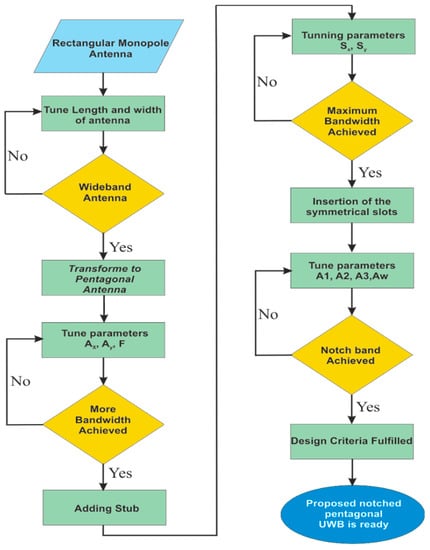
Figure 7.
Design and optimization procedure of the proposed antenna.
It is worth mentioning that the parametric sweep was done and optimized through a genetic algorithm (GA) due to its easy use and robustness within the CST Microwave Studio. By setting the design goals (a wide S11 bandwidth and high notching characteristics at the desired band) and designating the antenna parameters (input variable), the optimization was done quickly and efficiently. The block diagram of the GA is plotted in Figure 8. The details of the GA in antenna optimization can be found in [36].
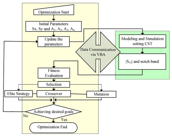
Figure 8.
Optimization of the antenna through a GA.
3. Results and Discussion
3.1. Measurement Setup
To accurately verify the frequency domain reflection characteristics of the proposed antenna, we used Vector Network Analyzer (VNA) test equipment. This instrument is essential to validate the antenna’s performance and obtains the best possible precision. The fabricated prototype of the proposed antenna is illustrated in Figure 9. A far-field measurement system in a shielded RF anechoic chamber was used to measure the far-field characteristics of the resulting antenna. The proposed antenna acted as a receiving antenna during the measurements. A standard horn antenna (SGH-Series) with a typical reference gain equal to 24 dBi was used as the transmitting antenna to deliver accurate and reliable antenna gain measurements. High gain power amplifiers were used in the antenna measurement to ensure the efficient transmission of the radio signal from the transmitter toward the receiver. This type of equipment boosts the signal generated by a voltage-controlled generator (VCO), which can be easily affected by transmission losses and open air. Therefore, using a power amplifier enables the receiving antenna to overcome these problems and provide the correct radiation pattern.
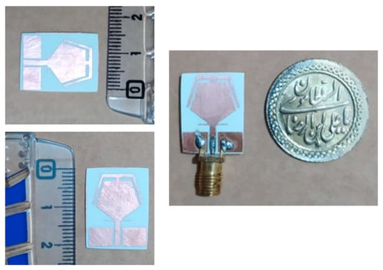
Figure 9.
Fabricated prototype of the proposed antenna.
3.2. Return Loss and VSWR
Figure 10a depicts the simulated and measured results of the proposed antenna. As can be seen, the simulation and measured results were in good agreement. The |S11| < −10 dB bandwidth of the resulting antenna ranged from 3.18 to 3.75 GHz and from 4.785 to 14.25 GHz; i.e., 180% of FBW in regard to the reference frequency of 5.25 GHz, which proved that the antenna successfully attenuated the desired sub-band from 3.75 to 4.875 GHz. In addition, the simulated and measured results showed a return loss coefficient of less than −20 dB, proving that the antenna was well matched to the source.
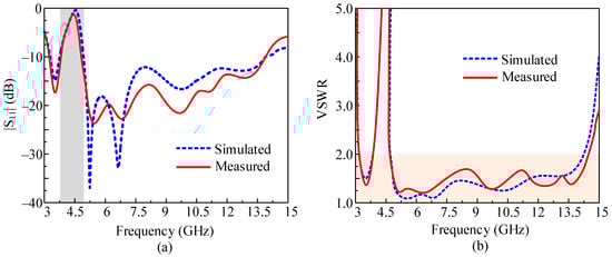
Figure 10.
Simulated and measured (a) return loss (b) VSWR of the proposed antenna.
Figure 10b illustrates the VSWR plot of both the simulated and measured results of the resulting antenna. As can be observed, the results were symmetrical and followed the same pace. Moreover, the figure shows that the antenna rejected a sub-band with a center frequency of 4.5 GHz and a maximum VSWR value of 38.
3.3. Radiation Pattern
Figure 11 illustrates the simulation and measured radiation pattern of the resulting antenna. As can be seen, the antenna exhibited an omnidirectional pattern in the H-plane (θ = 90°) and a bi-directional radiation pattern in the E-plane (θ = 0°). Moreover, we noticed that there was a good agreement between the simulation and measurement for both planes.
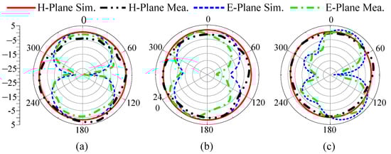
Figure 11.
Radiation patterns of the antenna: (a) 3.5 GHz, (b) 5.8 GHz and (c) 8 GHz.
3.4. Peak Gain and Efficiency
Figure 12 presents the gain and radiation efficiency plots of the final proposed antenna. The simulated and measured gain graphs were identical with a minimum value of −3.8 dBi at the center frequency (4.5 GHz) of the stop-band. In contrast, it showed a gradual increase in the rest of the operational band with a maximal gain value of 5.8 dBi beyond the frequency of 12 GHz. The reported results in this plot demonstrate that the sub-band ranging from 3.75 to 4.875 GHz was successfully attenuated, as was the radiation efficiency plot of the proposed antenna. As can be seen, the radiation efficiency presented a stable value of 98% all over the operational band except for the frequency range from 3.75 to 4.875 GHz, which was the spectrum portion we sought to mitigate.
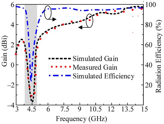
Figure 12.
Gain and radiation efficiency of the proposed antenna.
3.5. Comparison with State-of-the-Art Works
Table 2 illustrates a performance comparison between the proposed antenna and state-of-the-art antennas dedicated to the same applications. The antenna outperformed the existing antennas with its compact size, wider operating bandwidth, higher gain and stop-band functionality.
Table 2.
Performance comparison with state-of-the-art antennas.
4. Conclusions
The design and realization of a low-profile pentagonal compact antenna with a notch band characteristic were discussed in this paper. The shape of the radiating element was chosen to achieve a large bandwidth. The operating bandwidth was further improved by using a horizontal stub at the feedline. The proposed design was characterized by a low level of complexity and could easily be accommodated in future handheld devices. In addition, the proposed antenna was capable of attenuating an adjacent sub-band in the UWB region ranging from 3.75 to 4.87 GHz, which is used by the majority of communication standards and applications.
Author Contributions
Conceptualization, W.A.A.; methodology, software and validation, W.A.A. and A.Z.; formal analysis, investigation, resources and data curation, I.S., M.H. and N.H.; writing—original draft preparation, W.A.A. and A.Z.; writing—review and editing, W.A.A., M.H. and N.H.; supervision, project administration and funding acquisition, N.H. All authors have read and agreed to the published version of the manuscript.
Funding
This work is partially supported by Antenna and Wireless Propagation Group (https://sites.google.com/view/awpgrp), accessed on 15 august 2021.
Institutional Review Board Statement
Not applicable.
Informed Consent Statement
Not applicable.
Data Availability Statement
Not applicable.
Conflicts of Interest
The authors declare no conflict of interest.
References
- Malik, J.; Patnaik, A.; Kartikeyan, M. Compact Antennas for High Data Rate Communication; Springer: Cham, Switzerland, 2018. [Google Scholar] [CrossRef]
- Dougherty, E.R.; Shmulevich, I.; Chen, J.; Wang, Z.J. EURASIP Book Series on Signal Processing and Communications. In Genomic Signal Processing and Statistics; Hindawi Publishing Corporation: Cairo, Egypt, 2005; Volume 2, pp. 11–14. [Google Scholar]
- Guha, D.; Antar, Y.M. (Eds.) Microstrip and Printed Antennas: New Trends, Techniques and Applications; John Wiley & Sons: Hoboken, NJ, USA, 2011. [Google Scholar]
- Tseng, V.; Chang, C.-Y. Linear Tapered Slot Antenna for Ultra-Wideband Radar Sensor: Design Consideration and Recommendation. Sensors 2019, 19, 1212. [Google Scholar] [CrossRef] [PubMed] [Green Version]
- Baard, C.; Liu, Y.; Nikolova, N. Ultra-Wideband Low-Cost High-Efficiency Cavity-Backed Compound Spiral Antenna. Electronics 2020, 9, 1399. [Google Scholar] [CrossRef]
- Trinh-Van, S.; Kwon, O.H.; Jung, E.; Park, J.; Yu, B.; Kim, K.; Seo, J.; Hwang, K.C. A Low-Profile High-Gain and Wideband Log-Periodic Meandered Dipole Array Antenna with a Cascaded Multi-Section Artificial Magnetic Conductor Structure. Sensors 2019, 19, 4404. [Google Scholar] [CrossRef] [Green Version]
- Tampouratzis, M.G.; Vouyioukas, D.; Stratakis, D.; Yioultsis, T. Use Ultra-Wideband Discone Rectenna for Broadband RF Energy Harvesting Applications. Technologies 2020, 8, 21. [Google Scholar] [CrossRef] [Green Version]
- Lalbakhsh, A.; Afzal, M.U.; Hayat, T.; Esselle, K.P.; Mandal, K. All-metal wideband metasurface for near-field transformation of medium-to-high gain electromagnetic sources. Sci. Rep. 2021, 11, 9421. [Google Scholar] [CrossRef]
- Hayat, T.; Afzal, M.U.; Lalbakhsh, A.; Esselle, K.P. Additively Manufactured Perforated Superstrate to Improve Directive Radiation Characteristics of Electromagnetic Source. IEEE Access 2019, 7, 153445–153452. [Google Scholar] [CrossRef]
- Lalbakhsh, A.; Afzal, M.U.; Esselle, K.; Smith, S. A High-gain Wideband EBG Resonator Antenna for 60 GHz Unlicenced Frequency Band. In Proceedings of the 12th European Conference on Antennas and Propagation (EuCAP 2018), London, UK, 9–13 April 2018. [Google Scholar] [CrossRef]
- Lalbakhsh, A.; Afzal, M.U.; Esselle, K.P.; Smith, S.L. Low-Cost Nonuniform Metallic Lattice for Rectifying Aperture Near-Field of Electromagnetic Bandgap Resonator Antennas. IEEE Trans. Antennas Propag. 2020, 68, 3328–3335. [Google Scholar] [CrossRef]
- Mohamadzade, B.; Simorangkir, R.B.V.B.; Hashmi, R.M.; Lalbakhsh, A. A Conformal Ultrawideband Antenna with Monopole-Like Radiation Patterns. IEEE Trans. Antennas Propag. 2020, 68, 6383–6388. [Google Scholar] [CrossRef]
- Mohamadzade, B.; Simorangkir, R.B.V.B.; Hashmi, R.M.; Gharaei, R.; Lalbakhsh, A.; Shrestha, S.; Zhadobov, M.; Sauleau, R. A Conformal, Dynamic Pattern-Reconfigurable Antenna Using Conductive Textile-Polymer Composite. IEEE Trans. Antennas Propag. 2021, 1. [Google Scholar] [CrossRef]
- Chen, Z.; Lu, B.; Zhu, Y.; Lv, H. A Compact Printed Monopole Antenna for WiMAX/WLAN and UWB Applications. Future Internet 2018, 10, 122. [Google Scholar] [CrossRef] [Green Version]
- Samsuzzaman, M.; Islam, M.T. Circularly Polarized Broadband Printed Antenna for Wireless Applications. Sensors 2018, 18, 4261. [Google Scholar] [CrossRef] [Green Version]
- Li, K.; Dong, T.; Xia, Z. Wideband Printed Wide-Slot Antenna with Fork-Shaped Stub. Electronics 2019, 8, 347. [Google Scholar] [CrossRef] [Green Version]
- Siddiqui, J.Y.; Saha, C.; Antar, Y.M.M. Compact Dual-SRR-Loaded UWB Monopole Antenna with Dual Frequency and Wideband Notch Characteristics. IEEE Antennas Wirel. Propag. Lett. 2014, 14, 100–103. [Google Scholar] [CrossRef]
- Peng, L.; Wen, B.-J.; Li, X.-F.; Jiang, X.; Li, S.-M. CPW Fed UWB Antenna by EBGs with Wide Rectangular Notched-Band. IEEE Access 2016, 4, 9545–9552. [Google Scholar] [CrossRef]
- Rahman, M.; NagshvarianJahromi, M.; Mirjavadi, S.S.; Hamouda, A.M. Compact UWB Band-Notched Antenna with Integrated Bluetooth for Personal Wireless Communication and UWB Applications. Electronics 2019, 8, 158. [Google Scholar] [CrossRef] [Green Version]
- Ghaffar, A.; Awan, W.A.; Zaidi, A.; Hussain, N.; Rizvi, S.M.; Li, X.J. Compact Ultra Wide-Band and Tri-Band Antenna for Portable Device. Radioengineering 2020, 29, 601–608. [Google Scholar] [CrossRef]
- Kadam, A.A.; Deshmukh, A.A.; Ray, K.P. Slit Loaded Pentagon Shaped Ultra Wideband Antenna for Band Notch Characteristics. In Proceedings of the 2019 IEEE International Conference on Electrical, Computer and Communication Technologies (ICECCT), Coimbatore, India, 20–22 February 2019; pp. 1–6. [Google Scholar] [CrossRef]
- Touhami, N.A.; Yahyaoui, Y.; Zakriti, A.; Bargach, K.; Boussouis, M.; Lamsalli, M.; Tribak, A. A compact CPW-fed planar pentagon antenna for UWB applications. Prog. Electromagn. Res. 2014, 46, 153–161. [Google Scholar] [CrossRef] [Green Version]
- Awan, W.A.; Zaidi, A.; Hussain, N.; Iqbal, A.; Baghdad, A. Stub loaded, low profile UWB antenna with independently controllable notch-bands. Microw. Opt. Technol. Lett. 2019, 61, 2447–2454. [Google Scholar] [CrossRef]
- Jeong, M.J.; Hussain, N.; Bong, H.; Park, J.W.; Shin, K.S.; Lee, S.W.; Rhee, S.Y.; Kim, N. Ultrawideband microstrip patch antenna with quadruple band notch characteristic using negative permittivity unit cells. Microw. Opt. Technol. Lett. 2019, 62, 816–824. [Google Scholar] [CrossRef]
- Sun, Y.; Guo, T.; Wang, X.; Sun, R. The design for multi-frequency microstrip antenna based on gap-coupled. In Proceedings of the 2016 Progress in Electromagnetic Research Symposium (PIERS), Shanghai, China, 8–11 August 2016; pp. 1965–1967. [Google Scholar] [CrossRef]
- Abbas, A.; Hussain, N.; Jeong, M.-J.; Park, J.; Shin, K.S.; Kim, T.; Kim, N. A Rectangular Notch-Band UWB Antenna with Controllable Notched Bandwidth and Centre Frequency. Sensors 2020, 20, 777. [Google Scholar] [CrossRef] [PubMed] [Green Version]
- Madhav, B.T.P.; Rao, M.V.; Anilkumar, T. Conformal Band Notched Circular Monopole Antenna Loaded with Split Ring Resonator. Wirel. Pers. Commun. 2018, 103, 1965–1976. [Google Scholar] [CrossRef]
- Yadav, A.; Agrawal, S.; Yadav, R. SRR and S-shape slot loaded triple band notched UWB antenna. AEU—Int. J. Electron. Commun. 2017, 79, 192–198. [Google Scholar] [CrossRef]
- Iqbal, A.; Smida, A.; Mallat, N.K.; Islam, M.T.; Kim, S. A Compact UWB Antenna with Independently Controllable Notch Bands. Sensors 2019, 19, 1411. [Google Scholar] [CrossRef] [Green Version]
- Mirmosaei, S.S.; Afjei, E.; Mehrshahi, E.; Fakharian, M.M. A dual band-notched ultra-wideband monopole antenna with spiral-slots and folded SIR-DGS as notch band structures. Int. J. Microw. Wirel. Technol. 2015, 8, 1197–1206. [Google Scholar] [CrossRef]
- Abbosh, A.M.; Bialkowski, M.E. Design of UWB Planar Band-Notched Antenna Using Parasitic Elements. IEEE Trans. Antennas Propag. 2009, 57, 796–799. [Google Scholar] [CrossRef]
- Devana, V.N.K.R.; Rao, A.M. Design and Analysis of Dual Band-Notched UWB Antenna Using a Slot in Feed and Asymmetrical Parasitic stub. IETE J. Res. 2020, 1–11. [Google Scholar] [CrossRef]
- Guichi, F.; Challal, M.; Denidni, T.A. A novel dual band-notch ultra-wideband monopole antenna using parasitic stubs and slot. Microw. Opt. Technol. Lett. 2018, 60, 1737–1744. [Google Scholar] [CrossRef]
- Ullah, S.; Ruan, C.; Sadiq, M.S.; Haq, T.U.; Fahad, A.K.; He, W. Super wide band, defected ground structure (DGS), and stepped meander line antenna for WLAN/ISM/WiMAX/U.W.B. and other wireless communication applications. Sensors 2020, 20, 1735. [Google Scholar] [CrossRef] [PubMed] [Green Version]
- Balanis, C.A. Antenna Theory: Analysis and Design; John Wiley & Sons: Hoboken, NJ, USA, 2015. [Google Scholar]
- Haupt, R.L.; Haupt, S.E. Practical Genetic Algorithms; John Wiley: Hoboken, NJ, USA, 2004. [Google Scholar]
- Mandal, T.; Das, S. Design of a microstrip fed printed monopole antenna for bluetooth and UWB applications with WLAN notch band characteristics. Int. J. RF Microw. Comput. Eng. 2015, 25, 66–74. [Google Scholar] [CrossRef]
- Fang, R.; Song, R.; Zhao, X.; Wang, Z.; Qian, W.; He, D. Compact and Low-Profile UWB Antenna Based on Graphene-Assembled Films for Wearable Applications. Sensors 2020, 20, 2552. [Google Scholar] [CrossRef]
- Simorangkir, R.B.V.B.; Kiourti, A.; Esselle, K. UWB Wearable Antenna with a Full Ground Plane Based on PDMS-Embedded Conductive Fabric. IEEE Antennas Wirel. Propag. Lett. 2018, 17, 493–496. [Google Scholar] [CrossRef]
- Rahman, M.; Naghshvarianjahromi, M.; Mirjavadi, S.S.; Hamouda, A.M. Resonator Based Switching Technique between Ultra Wide Band (UWB) and Single/Dual Continuously Tunable-Notch Behaviors in UWB Radar for Wireless Vital Signs Monitoring. Sensors 2018, 18, 3330. [Google Scholar] [CrossRef] [PubMed] [Green Version]
Publisher’s Note: MDPI stays neutral with regard to jurisdictional claims in published maps and institutional affiliations. |
© 2021 by the authors. Licensee MDPI, Basel, Switzerland. This article is an open access article distributed under the terms and conditions of the Creative Commons Attribution (CC BY) license (https://creativecommons.org/licenses/by/4.0/).