Article

A Ku-Band RF Front-End Employing Broadband Impedance Matching with 3.5 dB NF and 21 dB Conversion Gain in 45-nm CMOS Technology

1
NICE Laboratory, School of Electrical Engineering, Korea Advanced Institute of Science and Technology (KAIST), Daejeon 34141, Korea
2
Department of Electronics and Control Engineering, Hanbat National University, Daejeon 34158, Korea
*
Author to whom correspondence should be addressed.
Electronics 2020, 9(3), 539; https://doi.org/10.3390/electronics9030539
Submission received: 26 February 2020 / Revised: 17 March 2020 / Accepted: 20 March 2020 / Published: 24 March 2020

Abstract

:
This paper presents a K u -band RF receiver front-end with broadband impedance matching and amplification. The major building blocks of the proposed receiver front-end include a wideband low-noise amplifier (LNA) employing a cascade of resistive feedback inverter (RFI) and transformer-loaded common source amplifier, a down-conversion mixer with push–pull transconductor and complementary LO switching stage, and an output buffer. Push–pull architecture is employed extensively to maximize the power efficiency, bandwidth, and linearity. The proposed two-stage LNA employs the stagger-tuned frequency response in order to extend the RF bandwidth coverage. The input impedance of RFI is carefully analyzed, and a wideband input matching circuit incorporating only a single inductor is presented along with useful equivalent impedance matching models and detailed design analysis. The prototype chip was fabricated in 45-nm CMOS technology and dissipates 78 mW from a 1.2-V supply while occupying chip area of 0.29 mm 2 . The proposed receiver front-end provides 21 dB conversion gain with 7 GHz IF bandwidth, 3.5 dB NF, −15.7 dBm IIP 3 while satisfying <−10 dB input matching over the whole input band.

1. Introduction

Many wireless communication standards have evolved, and continue to do so, in the millimeter-wave regime to accommodate an ever-increasing demand for various applications such as 5G communications, corresponding to which the number of devices is increasing, resulting in communication under heavily congested spectrum. Heavily congested spectrum entails the use of broadband spectrum sensing receiver for efficient and maximum utilization of the desired frequency spectrum.
The implementation of broadband sensing device is a difficult task with the major hurdles being the design of broadband amplifier and local oscillator (LO) signal synthesizer. All these parameters entail harsh design requirements with strict trade-offs, which are hard to meet simultaneously. At the system level, therefore, an architecture is required that can process broadband signals with less stringent design requirements.
RF channelization is an alluring method to achieve broadband spectrum sensing where the channelized receiver bifurcates the incoming RF band into multiple channels [1]. Ref. [2] presented the design challenges and requirements of channelized receiver operating from DC-40 GHz, where both series and parallel channelization concepts have been adopted to ease-off the requirements on RF front-end design for agile spectrum analysis.
Some of the previously reported works have proposed wideband receivers with good system performances. [3] reported a low-noise block (LNB) which down-converts the Ku-band (10.5–13 GHz) to the L-band (0.75–2.25 GHz). The system uses two-stage, narrow band cascode LNA topology, which requires a large number of inductors to achieve good input match along with high gain. The intense use of inductors in LNA and mixer in [3] renders the architecture unappealing in terms of area occupation. Similarly, [4] presented yet another LNB with system specifications similar to those in [3]. However, this work only provides amplification in a limited band, where the gain contribution from the LNA is the lowest. Moreover, the use of two-stage, inductor degenerated IF amplifier (used to compensate for the gain contribution from LNA) requires large area and high power consumption. L. Jia et al. [5] described a 10.7–12.75 GHz RF band front-end, implemented in 65-nm CMOS technology with the LNA using capacitive feedback to achieve wideband matching. However, as the results suggest, the proposed LNB fails to achieve <−10 dB input and output matching over the complete input RF band. Moreover, an external HEMT device with low noise figure (NF) of 0.45 dB and conversion gain of 10 dB has been employed to meet the NF requirements in [5]. It is worth mentioning that most of the earlier reported works have been designed for input RF bands with relatively narrow signal bandwidths (less than 3 GHz in most of the cases). This work, as the core building block of RF channelization receiver in [2], aims at the design and implementation of an extremely wideband RF front-end covering 10–20 GHz broad input bandwidth (which includes the whole K u -band) driven by 10 GHz local oscillator (LO) signal to donwconvert the input RF band to IF (intermediate frequency) with good dynamic range performance.
The paper is organized as follows. Section 2 reviews the receiver architecture for the 10–20 GHz band reception. Section 3 describes detailed analysis for designing the building blocks of the proposed receiver to achieve desired performance while maintaining adequate power efficiency. Section 4 provides the simulation and measurement results followed by the conclusion in Section 5.

2. Receiver Architecture

Figure 1 shows the complete architecture of the implemented receiver front-end. The proposed system consists of an LNA with both wideband input matching and signal amplification, an on-chip passive BALUN for single-ended to differential signal conversion along with action as a load of LNA, and down-conversion mixer. The 10 GHz LO signal is applied externally through two-stage inverter-based buffers. The down-converted IF signal in DC-10 GHz band is interfaced to off-chip 50 Ω termination through an output buffer.
The major considerations for 10–20 GHz receiver front-end include the NF, bandwidth, and conversion gain. With the broadband signal amplification required in the first stage of a receiver, LNA topology with minimum NF, large bandwidth, and maximum possible amplification are required. Moreover, mixing of LO and RF signal with minimum LO-IF and LO-RF feed-through is critical for zero-IF signal reception when this front-end is utilized for the channelization receiver [1,2].

3. Proposed Receiver Front-End

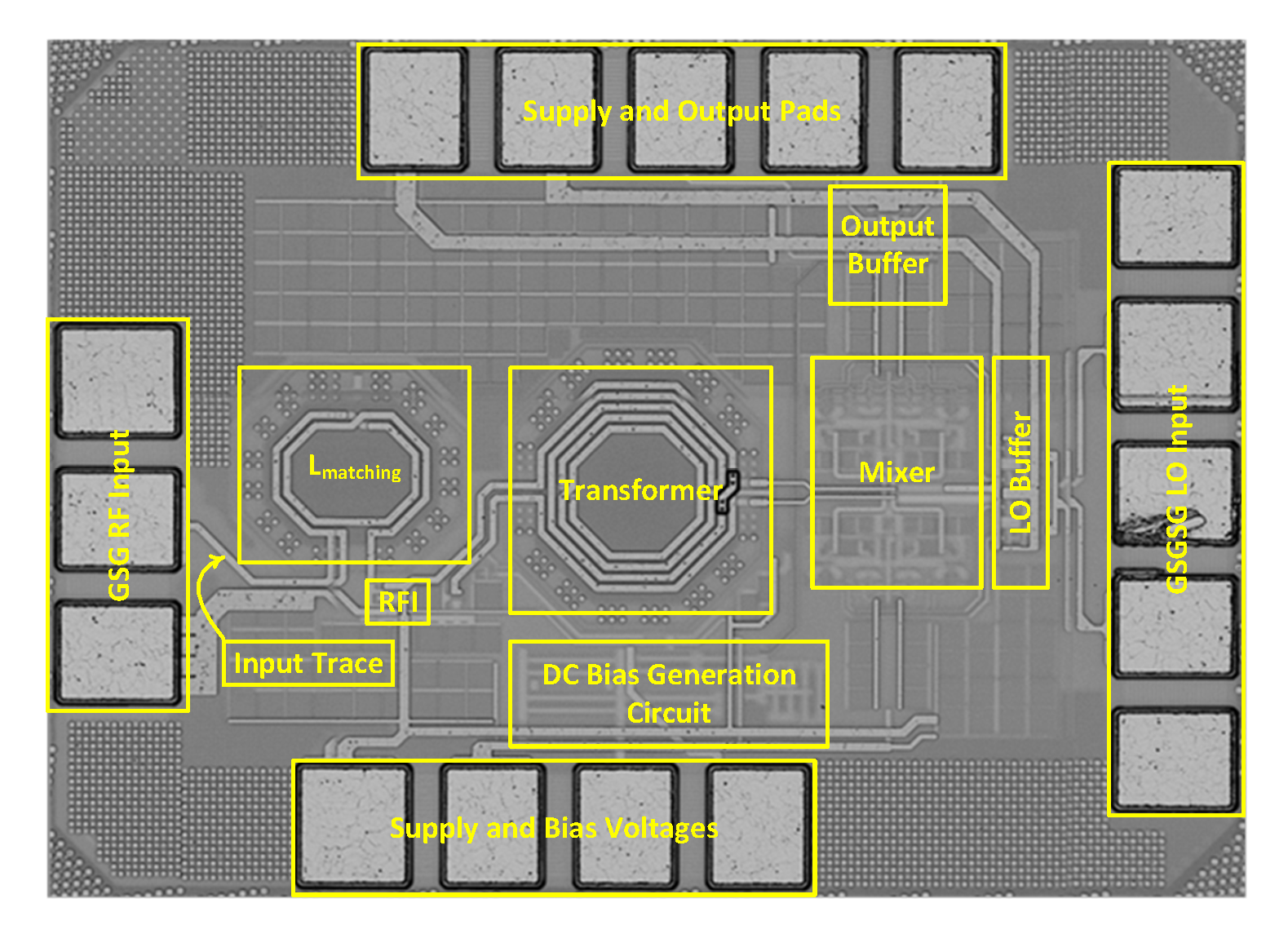
A description of the major building blocks, including wideband LNA and mixer, is given in the following sections.

3.1. Low Noise Amplifier (LNA)

Low-Noise Amplifier (LNA) with wide bandwidth is one of the most crucial components in designing receivers for instrumentation systems, optical communications, and software defined radios (SDR) [6]. Distributed Amplifiers (DA) were extensively used in the past to achieve high gain and broadband input matching. Several low power DA architectures have been proposed [7,8]; however, their main downside was occupation of large chip area. Hence, DAs have been deemed as an unsuitable choice for fully integrated receivers. The common source amplifier with inductive degeneration has been the most widely used topology to implement LNA [9], because of its high gain, good noise performance, and ability to match to the source impedance. However, inductor degenerated LNA is an inherently narrowband circuit topology with series RLC resonator as an input matching network [10]. Such an implementation provides high gain over a narrow band, and hence is not suitable for the broadband signal reception. Such a scheme can be adopted for wideband signaling provided that the power budget available for the whole system is high.
Resistive-feedback LNA provides high gain and broadband characteristics, along with good input matching, lower NF, and occupy small chip area [11]. 
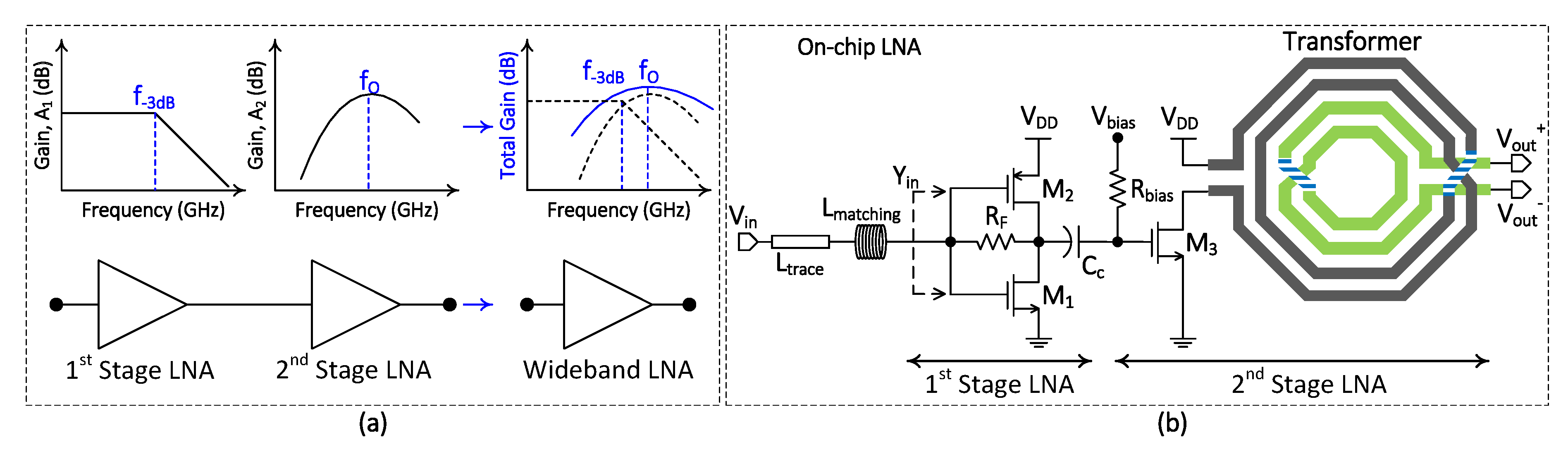
Figure 2a shows the architecture and design philosophy of the proposed two-stage wideband LNA. The two-stage topology ensures wideband signal reception by enhancing the LNA bandwidth using lowpass type first stage, and bandpass type second stage. The first stage enhances the low frequency content around the lower end of resonant frequency of the second stage, and combined together with the bandpass type second stage, guarantees wideband RF input signal reception and amplification. Figure 2b shows the schematic of proposed on-chip LNA. It consists of RFI as the first stage of LNA and a transformer-loaded common source amplifier as a second stage. The RFI can be thought of as an extension of resistive feedback common source amplifier, and can provide high linearity and good power efficiency as compared to its conventional counterpart, i.e., resistive feedback common source amplifier. As for the input matching to 50 Ω source, a single matching inductor, L m a t c h i n g , has been employed. According to the Friis NF equation [12], the NF of the overall system depends on the NF of the first stage, given that the gain of the first stage is adequately high. The DC gain of the RFI is given by:
A v = [ 1 R F G m ] [ r o n r o p ] 1 + r o n r o p R F
In Equation (1), G m = g m n + g m p , where g m n and g m p are the transconductances of the NMOS and PMOS devices in the RFI. Equation (1) states that the gain of the LNA can be increased by increasing the transconductance of both NMOS and PMOS devices. This is possible only if the output resistances of both NMOS and PMOS devices stay constant over device size variation. However, in short channel devices, by increasing the size of transistors to obtain high G m at the same DC current, the corresponding output resistances decrease and, hence, the intrinsic gain of the RFI stays relatively constant. The NF of the RFI is given by [13]:
N F = 1 + γ 1 G m R S + G m R S r o n r o p R F + r o n r o p 2 + 2 ( r o n r o p ) R F + r o n r o p
where R S is the source resistance and γ is the thermal noise coefficient for the NMOS and PMOS devices with values ranging from 1 to 2 in saturation condition. In short channel MOSFETs, the value of r o n r o p is usually very small, if the size of the transistors is chosen very large to increase the transconductance of the MOSFETs, and, hence, this value can drop below 100 Ω . Therefore, in Equation (2), if R F r o n r o p , then only the first term in the bracket will dominate. Accordingly, increasing the G m and satisfying R F r o n r o p condition simultaneously not only makes the gain of first stage LNA to approach its intrinsic gain, i.e., G m ( r o n r o p ) , but also reduces the NF of the overall system. It is important to note that Equation (2) only models the thermal noise effect of RFI and does not include 1 / f noise, and, hence, Equation (2) is constant for all frequencies. 
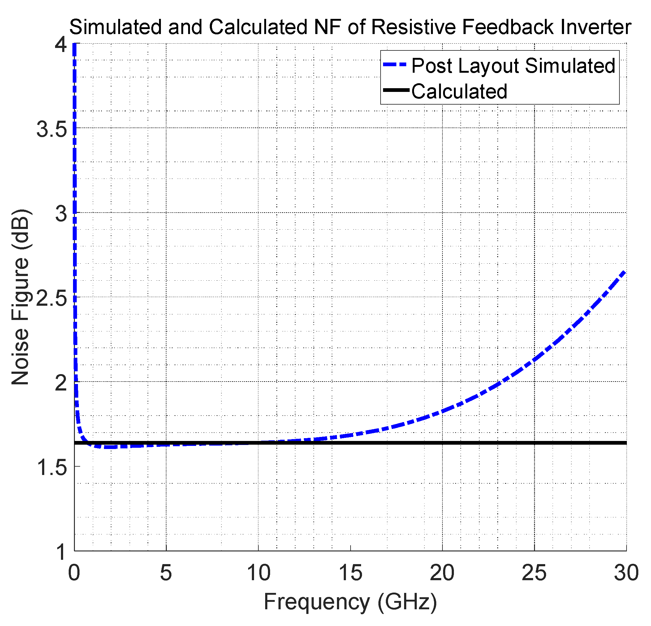
Figure 3 shows the calculated and simulated NF of the RFI based on the parameters given in Table 1. A good correlation between post-layout simulated NF of RFI and calculated NF can be seen from approximately 1 to 12 GHz based on the given NF model. Given that the circuit is properly designed, the RFI can provide a gain almost twice that of a conventional resistive feedback common source amplifier. This also indicates that the g m / I D efficiency of the RFI is better as compared to simple resistive feedback common source configuration owing to the utilization of current reuse technique. From a more rigorous analysis, it can be proven that, if R F R i n , then the amplifier is biased near V D D / 2 , which makes the amplifier linear and stable.
With the input signal having a 10 GHz bandwidth in this work, it is necessary that not only wideband amplification is achieved, but also the input of the LNA is matched to the source resistance over this whole frequency band to allow maximum power of the signal to be transferred to the LNA input. Hence, a wideband matching circuit needs to be designed as opposed to commonly employed narrowband matching techniques. Ref. [14] proposed a three-section bandpass Chebyshev filter to achieve ultrawideband input matching ranging 3.1–10.6 GHz RF input band. However, the proposed three-section filter employs three on-chip inductors to achieve wideband matching. It can be easily seen in [14] that the majority of the on-chip area has been occupied by the input matching network. One of the major focuses of this work is to alleviate this issue and achieve input matching with as few passive components as possible, provided that a slight compromise on the NF of whole system can be made.
G i n = 1 R i n = ( 1 + G m ( r o n r o p ) ) ( R F + r o n r o p + ω 2 C G D 2 R F 2 ( r o n r o p ) ) ( R F + r o n r o p ) 2 + ω 2 C G D 2 R F 2 ( r o n r o p ) 2
B i n = ω C i n = ω C G S ( R F 2 + ( r o n r o p ) 2 ) + 2 ω C G S R F ( r o n r o p ) + ω C G D R F 2 G m ( r o n r o p ) + ω 3 C G S C G D 2 R F 2 ( r o n r o p ) 2 ( R F + r o n r o p ) 2 + ω 2 C G D 2 R F 2 ( r o n r o p ) 2
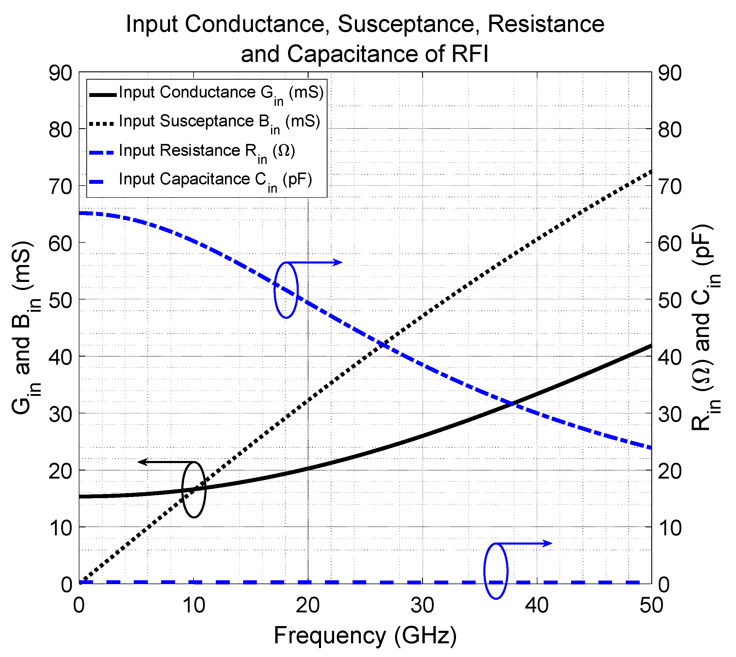
With only first-order approximations taken into account by ignoring the parasitic capacitances and gate resistance, the input admittance, Y i n = G i n + j B i n , of the RFI can be given by Equations (3) and (4), where C G S = C g s n + C g s p and C G D = C g d n + C g d p . It can be observed from Equation (3) that the real part of input impedance is dependent on the frequency. Hence, the transistors in RFI should be sized so that not only desirable gain and NF is achieved, but also an input conductance of around 20 mS is obtained within the input band of interest, i.e., from 10–20 GHz. Based on MATLAB simulations, Equations (3) and (4) are plotted in Figure 4. Based on the parameters given in Table 1, the input conductance, G i n , falls in the range of 16.6–20 mS in the desired input frequency band. Moreover, the input susceptance, B i n , increases almost linearly with frequency, which implies that the input admittance of the RFI can be modelled by a resistor in parallel with a capacitor. In Figure 4, the input resistance, R i n , and input capacitance, C i n , fall in the range from 60 to 49 Ω , and from 0.260 to 0.256 pF, respectively, based on the parameters chosen for transistor and other passive components in LNA. Combining this model of input admittance with the input matching inductor and a small pad capacitance results in a π -network. 
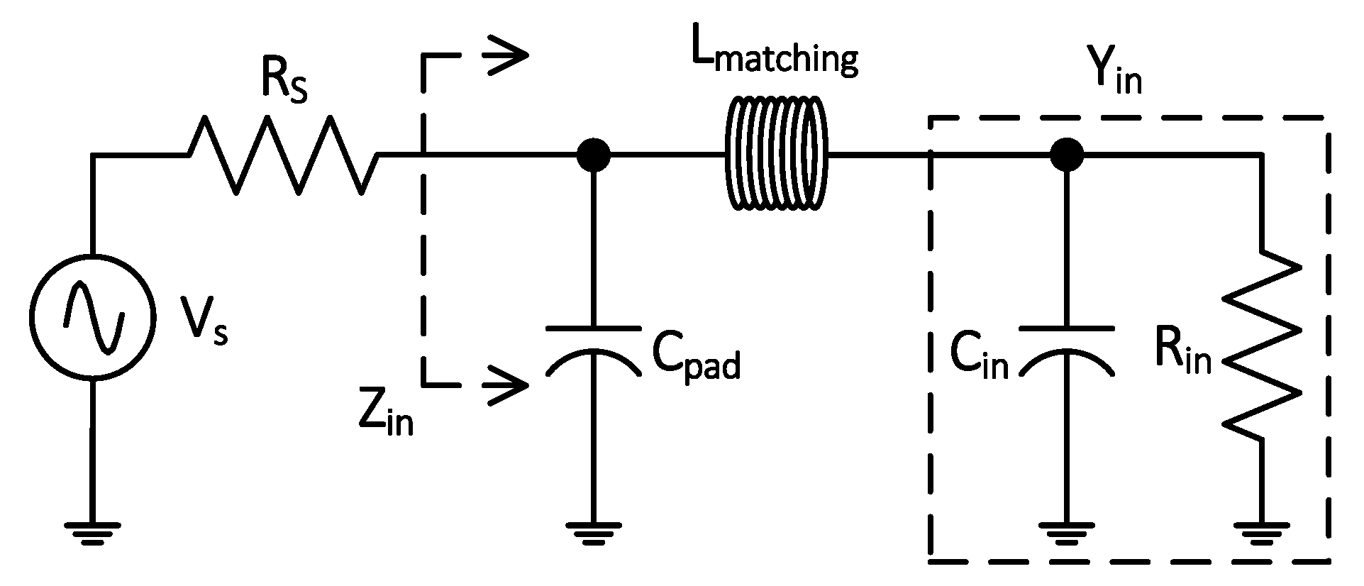
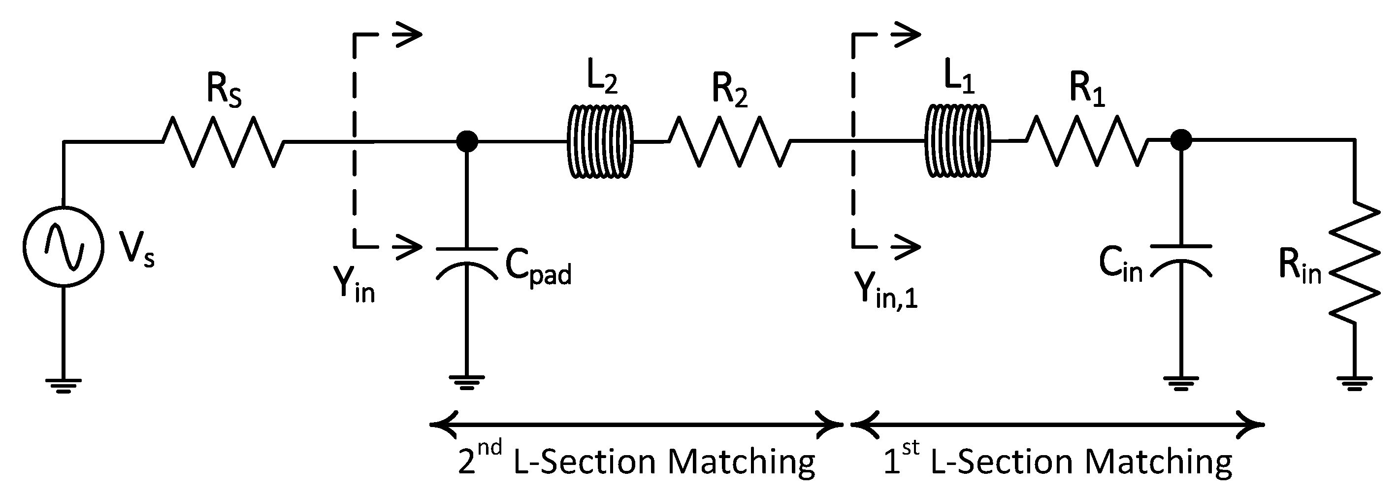
Figure 5 shows the equivalent model of the input matching circuit, i.e., L m a t c h i n g , along with the input admittance, Y i n , of RFI and the pad capacitance, C p a d . The input trace inductance, L t r a c e , connecting the input pad and the matching inductor has been ignored here for simplicity, and hence the value of L m a t c h i n g are evaluated at higher resonant frequencies relative to desired RF input band. Eventually, L t r a c e will shift the resonant band from higher end to the desired input band of 10–20 GHz. In the following, it is theoretically demonstrated that the proposed network can achieve wideband input matching with only a single matching inductor.
It is desired that the impedance, Z i n (or equivalently Y i n ), being seen at the input pad should be equal to R S (or equivalently 1 / R S if talking in terms of admittance parameters) over the whole input frequency band. The π -matching network can be designed by considering it as two cascaded L-section matching circuits, as described in Figure 6. It is important to note that R 1 and R 2 are the series resistances of their respective inductors. The 1 st L -section matching network tunes out C i n at a lower frequency, while the 2 nd L -section matching network tunes out C p a d at a higher frequency, since the value of pad capacitance is quite small. To tune out C i n at 15 GHz (which is the midpoint frequency of interest of the input band, and is hence called f o , l o w ), it is important to evaluate the value of the inductor L 1 along with its series resistance, R 1 , that can achieve such a task, and that value can be evaluated as per the following expression:
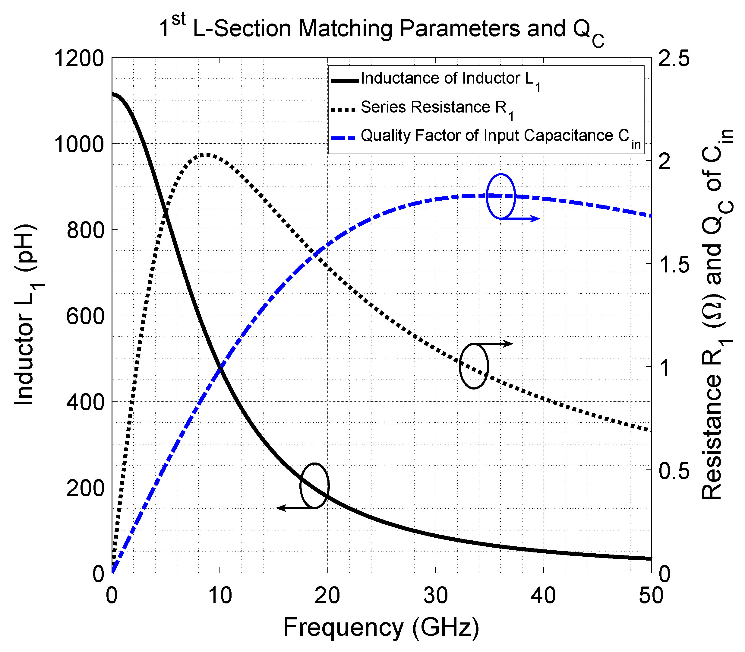
L 1 = R i n 2 C i n 1 + ω 2 R i n 2 C i n 2
R 1 = ω L 1 Q L 1
where Q L 1 = 15 is chosen as the quality factor of inductor L 1 . Having plotted Equations (5) and (6) in Figure 7, the desired value of L 1 to tune out C i n at 15 GHz is roughly equal to 280 pH. It is interesting to note, however, that the value of L 1 is frequency dependent and that Equation (5) provides freedom in choosing the value of L 1 which can tune out C i n at any desired frequency of interest. For instance, to tune out the C i n at 10 GHz, the required value of inductor would roughly be equal to 478 pH. The value of equivalent series resistance, R 1 , can be chosen based on Equation (6). In Figure 7, the value of R 1 is approximately equal to 1.76 Ω at f o , l o w 
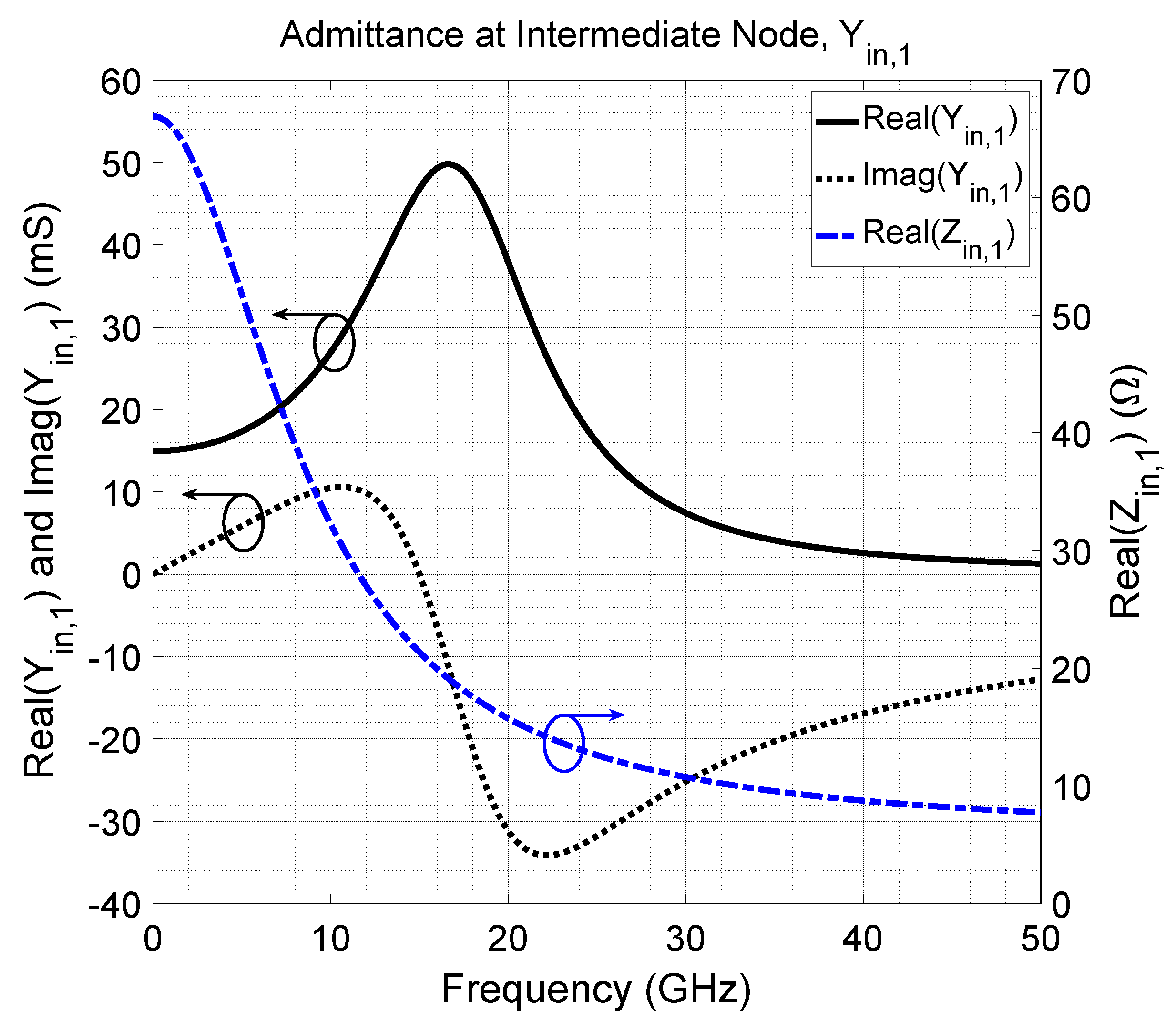
= 15 GHz. The input admittance and impedance at the intermediate node, Y i n , 1 , plotted in Figure 8, can be theoretically derived as:
Y i n , 1 = 1 Z i n , 1 = 1 + j ω R i n C i n R i n + ( R 1 + j ω L 1 ) ( 1 + j ω R i n C i n )
As evident in Figure 8, the chosen value for L 1 indeed tunes out C i n at desired resonant frequency, f o , l o w , which suggests that the input impedance at the intermediate node is composed purely of the resistive portion at f o , l o w , and is given by:
R i n , 1 = R i n 1 + Q C 2 + R 1
where Q C is the quality factor of C i n , also plotted in Figure 7. Equation (8) marks a reduction in series resistance being seen at the intermediate node at f o , l o w . With Q C = ω R i n C i n = 1.3 at f o , l o w , the value of input resistance is approximately halved as compared to R i n of RFI, where the input resistance varies from approximately 32 to 16 Ω at the intermediate node within the band of interest. However, the reactive part is zero only at f o , l o w and non-zero over rest of the frequency band, which illustrates that the total impedance being incorporated into the 2 nd L -section matching network is Z i n , 1 , where the value of Z i n , 1 at f o , l o w is given by Equation (8).
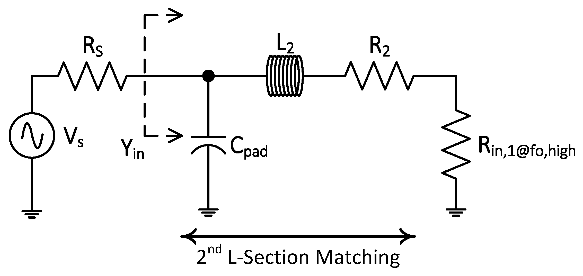
To ensure a good, wideband power match, it is vital that C p a d is also tuned out at f o , h i g h , and, to achieve it, the value of the inductor, L 2 , in the 2 nd L -section matching network must be sorted out. To tune out the C p a d , it is important that the total impedance, Z i n , 1 , being incorporated in 2 nd L -section matching network given by Equation (7), is purely resistive at f o , h i g h . As mentioned above, Figure 7 provides freedom in choosing the value of inductor L 1 to tune out C i n at any desired higher resonant frequency. At a frequency of 25 GHz (which is referred to as f o , h i g h ), the value of L 1 obtained in Figure 7 is roughly equal to 119 pH with the value of R 1 being equal to 1.25 Ω . This implies that at f o , h i g h , only resistive part will be incorporated into 2 nd L -section matching network, and the circuit at f o , h i g h would resemble the one in Figure 9. It is important to note that, at f o , h i g h , the total series resistance for L 2 has now increased from mere R 2 to R 2 = R 2 + R i n , 1 @ f o , h i g h . With the multiple unknowns being encountered, an initial assumption is required to evaluate the value of L 2 . As a starting point, it assumed that R 2 = a R 1 , where a is a multiplication factor ranging from as low as 1 to as high as required. By transforming the series R L circuit into parallel R L circuit in Figure 9, the values of equivalent components can be found by the subsequent equations:
R 2 , p a r a l l e l = ( R 2 + R 1 + R i n 1 + Q C 2 ) ( 1 + Q L 2 2 )
where R 1 , R i n , and Q C can be evaluated at f o , h i g h in Figure 4 and Figure 7. In this design, C p a d has been modeled by a 100 fF capacitance. The equivalent parallel inductance, L 2 , p a r a l l e l , can be found by:
L 2 , p a r a l l e l = 1 ω o , h i g h 2 C p a d
( R 1 + R 2 + R i n 1 + Q C 2 ) Q L 2 2 ( ω o , h i g h L 2 , p a r a l l e l ) Q L 2 + ( R 1 + R 2 + R i n 1 + Q C 2 ) = 0
The quality factor of the equivalent parallel inductor can be evaluated through Q L 2 = R 2 , p a r a l l e l / ( ω o , h i g h L 2 , p a r a l l e l ), and by substituting the values of Equation (9) in the aforementioned equation, a quadratic equation is obtained as mentioned in Equation (11). Solving Equation (11) yields two different values of Q L 2 from which the larger one would be employed in subsequent calculations. Having known the values of R 2 and Q L 2 , the required value of 2 nd L -section series matching inductor, L 2 , can be figured out through the following equation:
L 2 = Q L 2 R 2 ω o , h i g h
In the current design, having arbitrarily chosen the value of a = 10 along with the values of R 1 , R i n , and Q C at f o , h i g h , and L 2 , p a r a l l e l being obtained from Equation (10), Q L 2 is evaluated equal to 2.15 and from Equation (12), the value of L 2 is found equal to 333 pH. With the values of all the components evaluated, the input impedance, Z i n , at the source can be described by the following equation:
Z i n = 1 Y i n = j ω L 2 + R 2 + Z i n , 1 1 + j ω C p a d ( j ω L 2 + R 2 + Z i n , 1 )
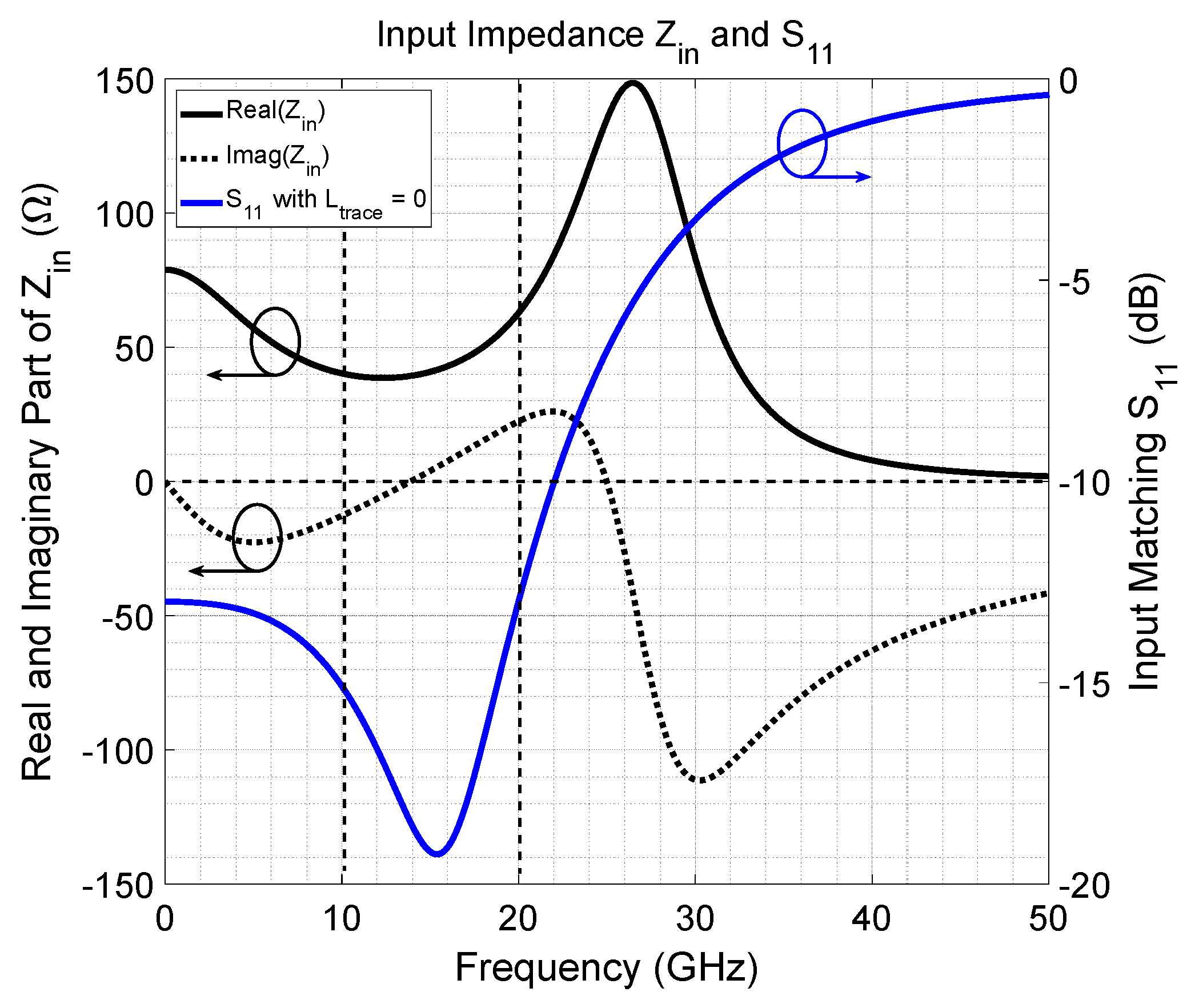
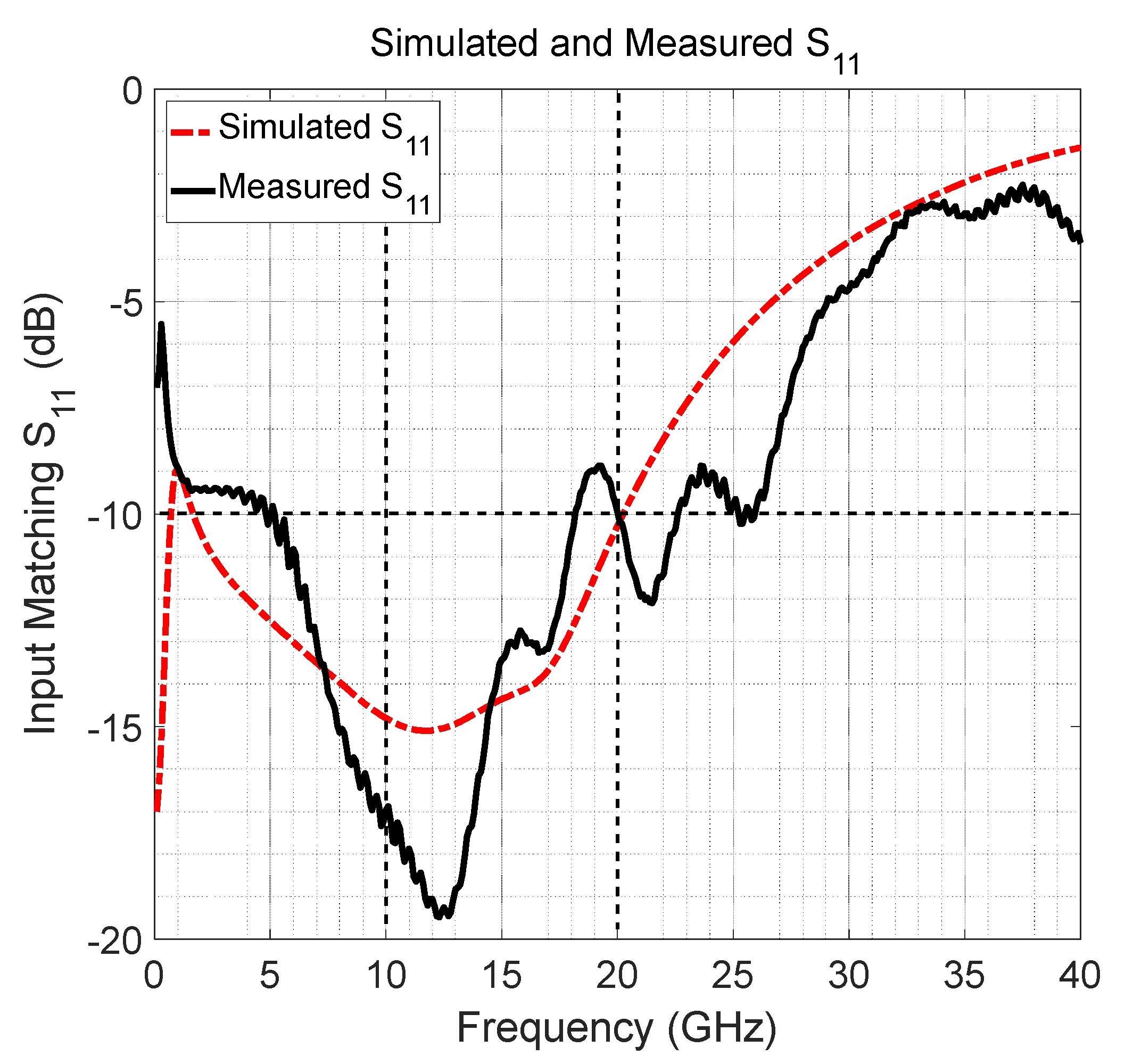
Figure 10 shows the MATLAB simulation plot of the input impedance, Z i n , and input matching, S 11 . In Figure 10, the input resistance seen by the source ranges from 40 to 63 Ω over the entire frequency band of 10–20 GHz, while the reactive portion ranges from −13 to 22 Ω . It can also be observed that the reactive portion of Z i n is zero at the desired resonant frequencies of 15 and 25 GHz. The effect of L t r a c e has been ignored in the aforementioned calculations. If the inductance of L t r a c e 
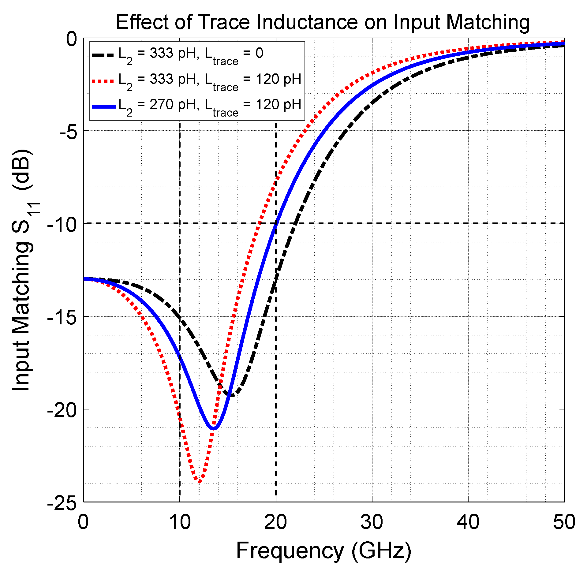
is taken into account, then the resonant frequency shifts towards the lower end of the input RF band, as shown in Figure 11. It can also be seen that the input matching no longer remains <−10 dB above 18 GHz. Hence, to compensate for this, the value of L 2 is reduced to 270 pH in the second iteration, which provides a perfect <−10 dB matching over whole input band. Having found the values of both the inductors at f o , h i g h , the value of an equivalent, single matching inductor can be found as follows:
L m a t c h i n g = L 1 , f o , h i g h + L 2 , f o , h i g h
From Equation (14), the value of an ideal, single equivalent matching inductor, L m a t c h i n g , is equal to 389 pH, which is equal to the one used in the actual design (value mentioned in Table 1). It must be noted that the value of L 1 evaluated previously was 280 pH. However, to resonate both C i n and C p a d , the total matching inductance value must satisfy Equation (14). In that case, if the value of L 1 was chosen to be 280 pH, then that of L 2 must be 109 pH as opposed to 270 pH. The quality factor of an equivalent, single matching inductor, L m a t c h i n g , can be calculated by:
Q m a t c h i n g = 2 π f o , h i g h L 1 , f o , h i g h R 1 + L 2 , f o , h i g h R 2
Therefore, apart from the input trace inductance (which is fixed because of the fixed length of the input signal line in the current design, but can be changed by laying out the chip in more efficient way so as to reduce L t r a c e ), a theoretical L m a t c h i n g value of 389 pH with a quality factor of approximately 18 is required to tune out both C i n and C p a d over a wide bandwidth of 10 GHz. A minor difference was observed in Z i n between the MATLAB simulation and actual design, which can be attributed to the unaccounted parasitics and first-order approximations made in evaluating the input admittance of RFI mentioned in Equations (3) and (4).
With implementation of the aforementioned input matching network and considering that the maximum signal power has been transferred to the input of the LNA, this whole band requires amplification. The first-stage LNA, i.e., RFI, cannot provide such a wideband signal amplification alone as it depicts a lowpass nature. In this work, the input signal is a bandpass type and, hence, an amplifier with bandpass characteristics is desired. The transformer-loaded common source amplifier has been adopted as the second stage, which is AC coupled with the previous stage and has its own biasing through the bias resistor, R b i a s , as shown in Figure 2. This configuration provides high gain in a narrow band (with its bandwidth dependent upon the quality factor of the transformer) around the resonant frequency, f o 
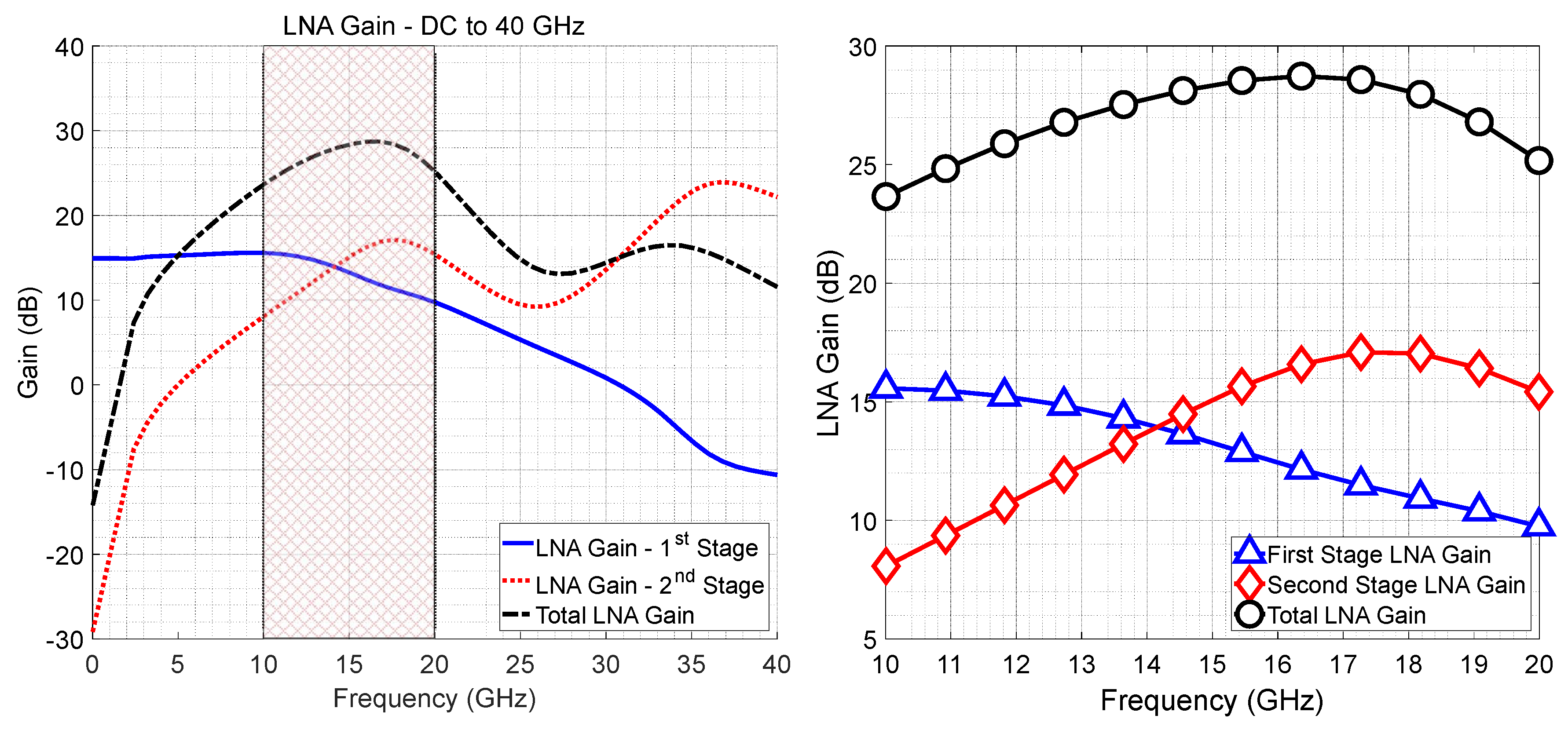
, which in this work is tuned towards the upper end of the input band. The proposed signaling method combining the lowpass and bandpass characteristics of first and second stage LNA, respectively, can thereby provide wideband signal amplification. The LNA gain plot has been shown in the 
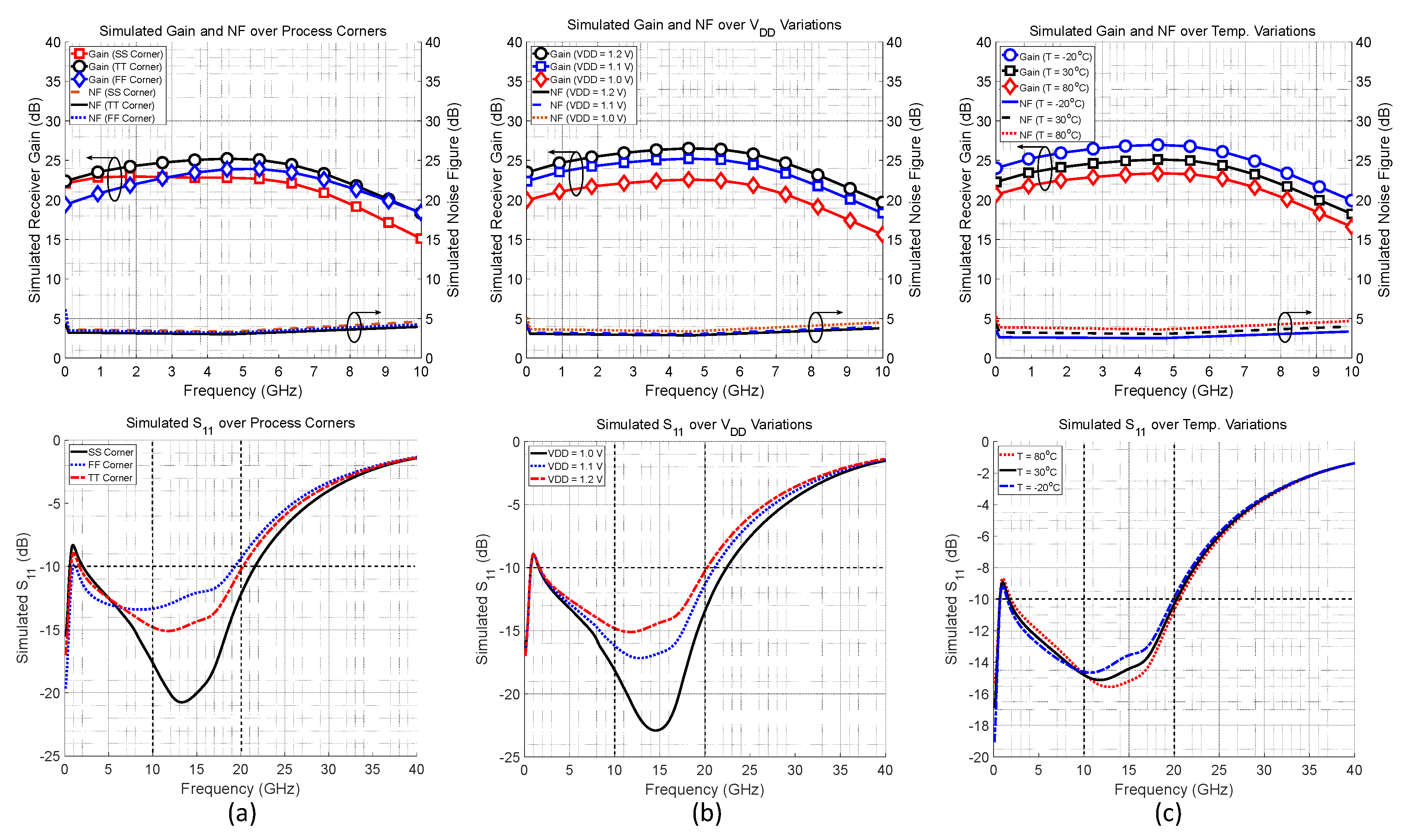
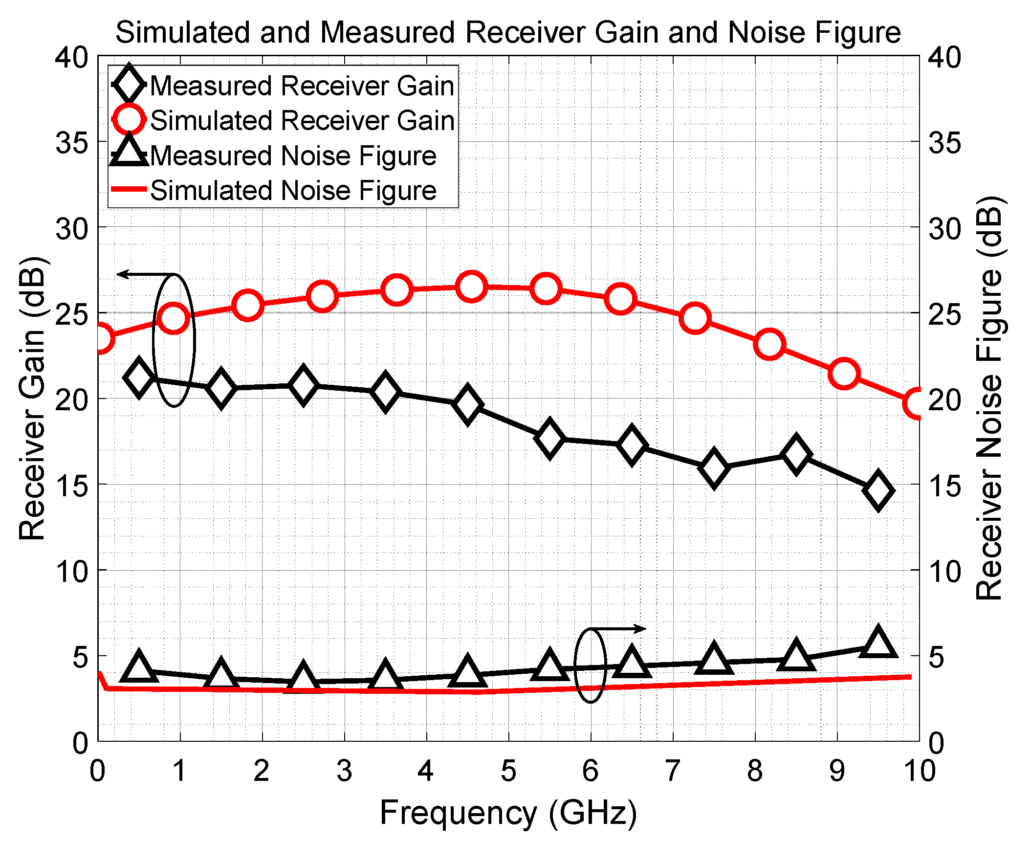
Figure 12. The 3-dB cutoff frequency of the first-stage LNA is 16.5 GHz (relative to 10 GHz), while the second-stage LNA is resonant at 18 GHz. The total LNA gain has been shown as a sum of gain from both stages where LNA provides a gain flatness of less than 4 dB. The transformer load also achieves single-to-differential conversion. Without the transformer load, high gain due to the front-end along with the parasitic ground inductance incurs unwanted oscillations. Another reason to convert the amplified signal from single-ended to differential is that the differential signaling in the mixer reduces the second-order distortions and improves robustness to power supply and substrate noise while also improving stability.
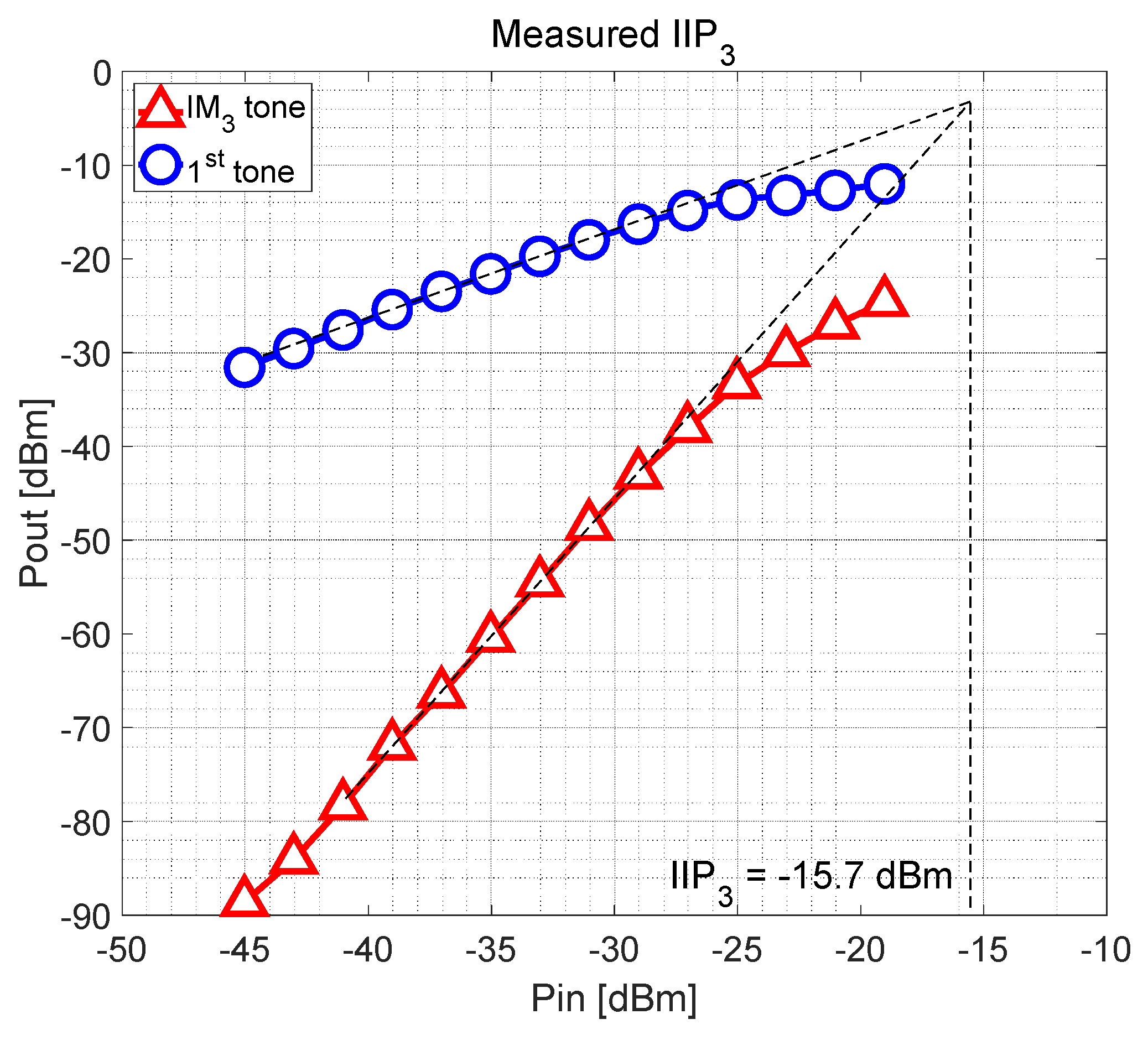
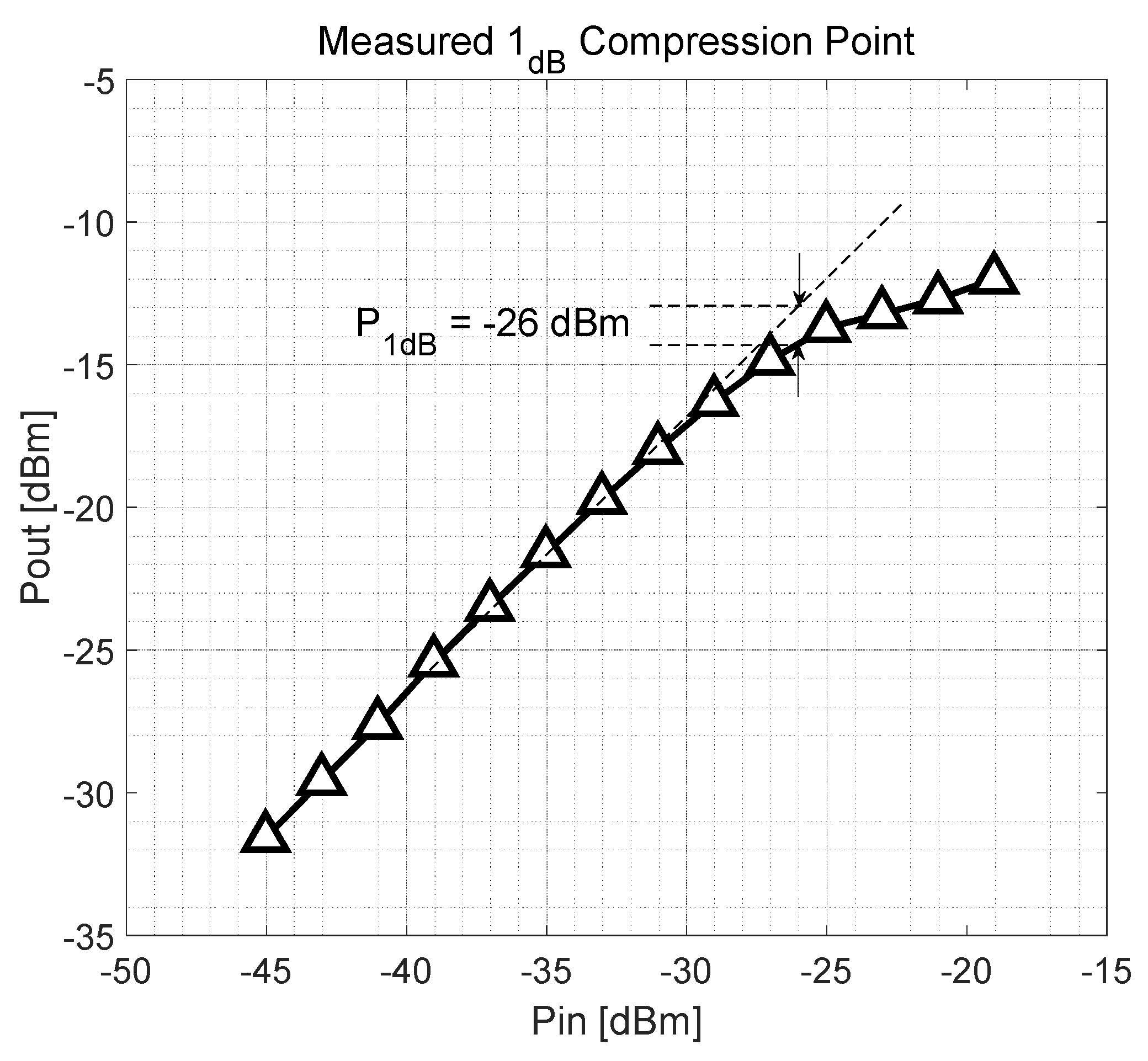
3.2. Mixer

Figure 13 shows the schematic diagram of a double balanced mixer where it has been implemented using a complementary switching and g m -stage [15]. The push–pull architecture improves both the g m -efficiency and noise performance, whereby also improving the linearity due to complementary input stage by eliminating the second order distortions [16]. This structure also improves the LO feedthrough to the output, which is extremely critical in this receiver front-end because the high-end frequency of the band coincides with the LO signal. Even though the push–pull single-balanced mixer architecture inherently performs single-to-differential conversion, transformer load for the LNA is utilized to perform single-to-differential conversion to utilize double-balanced mixer configuration. The double balanced mixer operation ensures stability by mitigating the effect of parasitic ground loops. Current-efficiency is maintained due to the complementary g m -stage even with the double-balanced mixer structure. Table 2 presents the mixer sizing parameters along with the values of passive components employed.
Along with its inherent ability to reduce the LO feedthrough to the output, the common-mode feedback (CMFB) circuit further reduces the LO-IF feedthrough by mitigating the mismatch between the complementary g m , i.e., g m n and g m p . The overall conversion gain of the implemented mixer can be derived as follows:
A C G = 2 π ( g m n + g m p ) R L 1 + s R L C e q
where R L is the load resistance connected at the output terminal, C e q is the total load capacitance, and g m n and g m p are the transconductances of the RF input voltage to current converters.
Considering that the input to the mixer is of bandpass type, ideally, a wideband mixer is desired so that it can downconvert the whole band to the desired IF band with minimum conversion loss. However, the RC time constant of the mixer appears as the main limitation in achieving wideband downconversion, as shown in Figure 14, where the mixer demonstrates a lowpass nature. The 3-dB IF bandwidth of the mixer is approximately equal to 4.66 GHz, and, above 7 GHz, the mixer shows conversion loss. This loss will manifest itself as overall gain loss of the system at frequencies above 7 GHz, as discussed below.
Assuming that the transconductances of the RF input NMOS and PMOS devices are same, the implemented mixer provides twice the conversion gain as compared to the conventional mixer topologies. The gain-bandwidth (GBW) product of the mixer can be derived as follows:
G B W = 2 π g m n + g m p C e q
where the equation implies that the GBW of the double balanced mixer with complementary LO and g m stages is better as compared to the conventional double-balanced mixer. The g m / I D efficiency of the mixer is also better as compared to its conventional counterparts, since the effective g m of the mixer is almost twice that of the normal mixer.

4. Measurement Results

The proposed ultra-wideband 10–20 GHz receiver front-end has been implemented in standard 45-nm CMOS technology. Figure 15 shows the fabricated chip micrograph having an occupied area of 0.29 mm 2 . For measurement purpose, IF output and DC pads are wire bonded to PCB with a FR4 substrate while RF and LO signals are applied using on-wafer probing to minimize the losses and mismatches. The final measurement results are presented after de-embedding the PCB trace loss and the loss of cables from source to DUT and DUT to spectrum analyzer. The entire circuit consumes 78 mW from a 1.2-V power supply.
Figure 16 shows the post-layout simulation results of the proposed receiver over PVT variations. Figure 16a shows the variation in receiver gain, NF, and S 11 over the global process corners (FF, TT, and SS). From the simulation results, the receiver gain is degraded at lower frequencies in FF corner relative to TT, while the degradation effect in the receiver gain is pronounced more at higher end of the IF band in SS corner as compared to the TT corner. The NF of the receiver degrades as one moves from TT to SS corner. However, the NF degradation is not severe over the global corner variations with the N F m i n staying below 4 dB. The S 11 plot indicates that the resonant frequency shifts towards higher frequency at SS corner in comparison to other corners but provides better matching. At the FF corner, the resonance frequency stays approximately the same as that in TT corner, but the amount of matching is relatively reduced. It is, however, encouraging to note that, within the band of interest (10–20 GHz), the input matching is still <−10 dB over all the corners. Figure 16b shows the receiver performance parameters over power supply variations. The power supply was varied from 1 to 1.2 V. As evident, reducing V D D not only reduces receiver gain over the whole band, but also degrades the NF. Similarly, input matching variations are shown, and, again, the input matching stays below <−10 dB over the supply variations within the band of interest. Figure 16c shows the performance parameters against temperature variations, where the gain, NF, and S 11 were measured at −20, 30, and 80 °C. Evidently, a rise in temperature degrades the performance of receiver in terms of gain and NF. However, the input matching is considerably tolerant to the temperature changes.
Figure 17 shows the simulated and measured conversion gain and NF results, respectively. The measurement results show a low frequency conversion gain of 21 dB as opposed to 24 dB obtained from the simulation, whereby the gain drops in an approximately linear fashion. Moreover, from the measured conversion gain, it was observed that the bandpass characteristic of the front-end has changed to lowpass characteristic. This indicates a shift in the resonant frequency of second stage LNA towards the lower end. The major reasons for the gain drop can be attributed to the IF output taken through SMA connector. From the electromagnetic simulation of a 50- Ω transmission line (TL) mounted on FR4 substrate, it was observed that the TL shows good impedance characteristics up to 5 GHz, after which the impedance of the TL deviates from the ideal behavior and does not provide characteristic impedance of 50 Ω from thereon. The NF results show that the integrated NF over whole IF band, i.e., 0–10 GHz, is 3.2 and 4.3 dB for simulation and measurement, respectively, with a minimum measured NF of 3.5 dB.
Figure 18 shows the input reflection coefficient, S 11 . The measurement results show that input of the receiver is matched ( S 11 < −10 dB) to the source over a wide band of 10–20 GHz, with a little discrepancy observed at the higher end from around 18 to 20 GHz.
Figure 19 shows the linearity performance of the front-end. The measured IIP 3 is −15.7 dBm based on two-tone signal injected at 15.1 and 15.2 GHz, with the LO power set at 0 dBm and RF power swept from −45 to −15 dBm. Clearly, IIP 3 of the receiver shows poor linearity with the significant IIP 3 degradation occurring because of the active mixer. The cascaded NF and IIP 3 equation indicates a trade-off between the linearity and NF. To achieve a relatively higher linearity, a passive mixer could be implemented, which would effectively degrade the system NF, a totally undesired effect in the proposed receiver. Figure 20 shows the measured 1-dB compression point. The implemented front-end shows a 1-dB compression point of approximately −26 dBm, 10.3 dB lower as compared to IIP 3 , which is quite close to the theoretical difference of 9.6 dB [17].
Table 3 presents the performance summary of this work in comparison to the related works. Considering that the input is a broadband 10 GHz signal as opposed to most of the referred work, in terms of NF, power consumption, bandwidth coverage, and area occupation, the proposed receiver provides competitive performance as compared to the cited works. The work in [18] has similar performance to the proposed receiver in terms of input matching, IIP 3 , and power consumption, but the input signal bandwidth is extremely small with the input band centered at 24 GHz. The NF is also almost double as compared to the proposed work. The 12–20 GHz receiver in [19] accomplishes good wideband reception and linearity with gain performance similar to the proposed work, but is inferior in terms of NF, input matching, and power consumption. Similarly, [20] proposed a receiver with superior power consumption and gain as compared to the proposed receiver, but it has a relatively narrowband reception of 1.48 GHz and poor NF. Even though the gain of the receiver in [21] is 53 dB over the 10 GHz bandwidth, the actual gain from the front-end is still 21 dB, where rest of the gain is provided by a baseband VGA. It is important to note that gain in almost half of the referred works in around 50 dB, which is due to the narrow RF input band. It is relatively difficult to achieve such a high gain over a broadband RF signal. The works presented in [22,23] provide extremely competitive receiver architectures with high gain, low NF, and low DC power consumption. However, these receivers provide such performance parameters over a relatively narrow bandwidth of 2.7 GHz. Similarly, the works in [24,25] provide competitive LNA architectures over extremely wide RF bandwidths. However, based on the post-layout simulation results, the proposed LNA provides even better performance in terms of gain, NF, and input matching as compared to these works. Therefore, as mentioned above, the most important parameters to measure the relative performance of the receivers is NF and input matching over the whole RF input band, in which case the proposed receiver stands out as compared to related works.

5. Conclusions

A 10–20 GHz band RF front-end has been implemented in a commercial 45-nm CMOS process. The prototype receiver front-end achieves broadband signal reception while maintaining good signal to noise ratio. The proposed architecture is suitable as the front-end solution of the broadband spectrum-sensing device. A complementary transconductor scheme is applied to the LNA as well as the down-conversion mixer, which improves the power efficiency while maintaining the performance. Stagger-tuned two-stage LNA implementation ensures the broadband signal amplification. The proposed receiver achieves a maximum conversion gain of 21 dB; a minimum and integrated NF of 3.5 and 4.3 dB, respectively; −15.7 dBm IIP 3 ; and less than −10 dB input matching over the entire RF input band from 10 to 20 GHz. The whole chip occupies 0.29 mm 2 area while consuming 78 mW power from 1.2-V supply.

Author Contributions

Conceptualization and design, D.R.U. and J.K.; analysis and draft preparation, H.U.M.; supervision, S.-K.H. and S.-G.L.; and funding acquisition, J.K. All authors have read and approved the final manuscript.

Funding

This work was supported by the research fund of Hanbat National University in 2019.

Conflicts of Interest

The authors declare no conflict of interest.

References

  1. Hsieh, T.-L.; Kinget, P.; Gharpurey, R. A rapid interference detector for ultra wideband radio systems in 0.13-μm CMOS. In Proceedings of the IEEE Radio Frequency Integrated Circuits (RFIC) Symposium, Atlanta, GA, USA, 15–17 June 2008. [Google Scholar]
  2. Kim, J.; Utomo, D.R.; Dissanayake, A.; Han, S.-K.; Lee, S.-G. The Evolution of Channelization Receiver Architecture: Principles and Design Challenges. IEEE Access 2017, 5, 25385–25395. [Google Scholar] [CrossRef]
  3. Deng, Z.; Chen, J.; Tsai, J.S.-H.; Niknejad, A.M. A CMOS Ku-band single-conversion receiver low-noise block front-end for satellite receivers. In Proceedings of the IEEE Radio Frequency Integrated Circuits (RFIC) Symposium, Boston, MA, USA, 7–9 June 2009. [Google Scholar]
  4. Kirkman-Bey, M.D.; Cintron-Tirado, P.N.; Sebsebie, R.; Dogan, N.S.; Xie, Z. Design and simulation of Ku-band low-noise block downconverter in 0.18 micrometer CMOS technology. In Proceedings of the IEEE SOUTHEASTCON 2014, Lexington, KY, USA, 13–16 March 2014. [Google Scholar]
  5. Jia, L.; Arasu, M.A. CMOS Ku-band LNB with high image suppression capability for satellite application. In Proceedings of the IEEE International Symposium on Integrated Circuits, Singapore, 12–14 December 2012. [Google Scholar]
  6. Kim, J.; Silva-Martinez, J. Low-power, low-cost CMOS direct conversion receiver front-end for multistandard applications. IEEE JSSC 2013, 48, 2090–2103. [Google Scholar]
  7. Yu, Y.-H.; Chen, Y.-J.E.; Heo, D. A 0.6-V low power UWB CMOS LNA. IEEE MWCL 2007, 17, 229–231. [Google Scholar] [CrossRef]
  8. Zhang, F.; Kinget, P.R. Low-power programmable gain CMOS distributed LNA. IEEE JSSC 2006, 41, 1333–1343. [Google Scholar] [CrossRef]
  9. Shaeffer, D.K.; Lee, T.H. A 1.5-V, 1.5 GHz CMOS low noise amplifier. IEEE JSSC 1997, 32, 745–759. [Google Scholar] [CrossRef] [Green Version]
  10. Kim, J.; Hoyos, S.; Silva-Martinez, J. Wideband common-gate CMOS LNA employing dual negative feedback with simultaneous noise, gain, and bandwidth optimization. IEEE TMTT 2010, 58, 2340–2351. [Google Scholar] [CrossRef]
  11. Chen, M.; Lin, J. A 0.1–20 GHz low-power self-biased resistive-feedback LNA in 90 nm digital CMOS. IEEE MWCL 2009, 19, 323–325. [Google Scholar] [CrossRef]
  12. Friis, H.T. Noise figures of radio receivers. Proc. IRE 1944, 32, 419–422. [Google Scholar] [CrossRef]
  13. Park, J.-Y.; Lee, J.-Y.; Yeo, C.-K.; Yun, T.-Y. Analysis and optimization of a resistive-feedback inverter LNA. MOTL 2018, 60, 1143–1151. [Google Scholar] [CrossRef]
  14. Bevilacqua, A.; Niknejad, A.M. An ultrawideband CMOS low-noise amplifier for 3.1–10.6 GHz wireless receivers. IEEE JSSC 2004, 39, 2259–2268. [Google Scholar] [CrossRef]
  15. Liu, Y.-H.; Huang, X.; Vidojkovic, M.; Ba, A.; Harpe, P.; Dolmans, G.; de Groot, H. A 1.9 nJ/b 2.4 GHz multistandard (Bluetooth Low Energy/Zigbee/IEEE802.15.6) transceiver for personal/body-area networks. In Proceedings of the IEEE Solid-State Circuits Conference Digest of Technical Papers, San Francisco, CA, USA, 17–21 February 2013. [Google Scholar]
  16. Fu, C.-T.; Lakdawala, H.; Taylor, S.S.; Soumyanath, K. A 2.5GHz 32nm 0.35mm2 3.5dB NF -5dBm P1dB Fully Differential CMOS Push-Pull LNA with Integrated 34dBm T/R Switch and ESD Protection. In Proceedings of the 2011 IEEE International Solid-State Circuits Conference, San Francisco, CA, USA, 20–24 February 2011. [Google Scholar]
  17. Razavi, B. RF Microelectronics; Prentice Hall: Upper Saddle River, NJ, USA, 1998. [Google Scholar]
  18. Mazzanti, A.; Sosio, M.; Repossi, M.; Svelto, F. A 24 GHz subharmonic direct downconversion receiver in 65 nm CMOS. IEEE TCAS–I Regul. Pap. 2011, 58, 88–97. [Google Scholar]
  19. Cheng, D.; Li, L.; Xie, M.; Sheng, B.; You, X. A Ku-band receiver with 12–to–20–dB gain, -14–dBm IP1dB in 65-nm CMOS technology. In Proceedings of the 2018 Asia-Pacific Microwave Conference, Kyoto, Japan, 6–9 November 2018. [Google Scholar]
  20. Wang, Y.; Lou, L.; Chen, B.; Zhang, Y.; Tang, K.; Qiu, L.; Liu, S.; Zheng, Y. A 260-mW Ku-band FMCW transceiver for synthetic aperture radar sensor with 1.48-GHz bandwidth in 65-nm CMOS technology. IEEE TMTT 2017, 65, 4385–4399. [Google Scholar] [CrossRef]
  21. Ma, D.; Dai, F.F.; Jaeger, R.C.; Irwin, J.D. An X-and Ku-band wideband recursive receiver MMIC with gain-reuse. IEEE JSSC 2011, 46, 562–571. [Google Scholar] [CrossRef]
  22. Hedayati, H.; Lau, W.-F.A.; Kim, N.; Aparin, V.; Entesari, K. A 1.8 dB NF blocker-filtering noise-canceling wideband receiver with shared TIA in 40 nm CMOS. IEEE JSSC 2015, 50, 1148–1164. [Google Scholar] [CrossRef]
  23. Murphy, D.; Hafez, A.; Mirzaei, A.; Mikhemar, M.; Darabi, H.; Chang, M.-C.F.; Abidi, A. A blocker-tolerant wideband noise-canceling receiver with a 2dB noise figure. In Proceedings of the IEEE International Solid-State Circuits Conference (ISSCC), San Francisco, CA, USA, 19–23 February 2012. [Google Scholar]
  24. Yu, H.; Chen, Y.; Boon, C.C.; Li, C.; Mak, P.-I.; Martins, R.P. A 0.044-mm2 0.5–to–7- GHz Resistor-Plus-Source-Follower-Feedback noise-canceling LNA achieving a flat NF of 3.3 ± 0.45 dB. IEEE TCAS-II Express Briefs 2019, 66, 71–75. [Google Scholar]
  25. Yu, H.; Chen, Y.; Boon, C.C.; Mak, P.-I.; Martins, R.P. A 0.096-mm2 15–20- GHz triple-path noise-canceling Common-Gate Common-Source LNA with dual complementary pMOS-nMOS configuration. IEEE TMTT 2020, 68, 144–159. [Google Scholar] [CrossRef]
  26. Wang, P.-Y.; Chou, M.-C.; Su, P.-C.; Chang, Y.-C.; Chuang, K.-H.; Hsu, S.S.H. A fully integrated Ku-band down-converter front-end for DBS receivers. In Proceedings of the IEEE MTT-S International Microwave Symposium, Tampa, FL, USA, 1–6 June 2014. [Google Scholar]
Figure 1. Proposed receiver architecture.
Electronics 09 00539 g001
Figure 2. (a) LNA architecture and design philosophy; and (b) schematic of two-stage LNA with resistive feedback inverter (RFI) as first stage, and transformer-loaded common source configuration as second stage.
Electronics 09 00539 g002
Figure 3. Calculated and simulated NF of RFI.
Electronics 09 00539 g003
Figure 4. Input conductance ( G i n ) and susceptance ( B i n ) of the RFI.
Electronics 09 00539 g004
Figure 5. Equivalent model of input matching circuit accounting for the parallel input resistance and capacitance, R i n and C i n , respectively, along with pad capacitance, C p a d .
Electronics 09 00539 g005
Figure 6. π -matching network thought of as cascaded L-section matching networks.
Electronics 09 00539 g006
Figure 7. Inductor L 1 and resistance R 1 vs. frequency.
Electronics 09 00539 g007
Figure 8. Admittance and resistance at intermediate node, Y i n , 1 .
Electronics 09 00539 g008
Figure 9. Desired circuit configuration at f o , h i g h .
Electronics 09 00539 g009
Figure 10. Input impedance and matching at the source.
Electronics 09 00539 g010
Figure 11. Effect of L t r a c e on input matching.
Electronics 09 00539 g011
Figure 12. Simulated LNA gain with individual contribution from first and second stages: extending from DC to 40 GHz (left); and zoomed-in version from 10 to 20 GHz (right).
Electronics 09 00539 g012
Figure 13. Double balanced mixer with complementary LO switching and g m -stage (left); and common-mode feedback circuit (right).
Electronics 09 00539 g013
Figure 14. Simulated conversion gain of the implemented mixer.
Electronics 09 00539 g014
Figure 15. Chip micrograph.
Electronics 09 00539 g015
Figure 16. (a) Simulated receiver gain, NF, and S 11 over global process corner variation; (b) simulated receiver gain, NF, and S 11 over power supply variation; and (c) simulated receiver gain, NF, and S 11 over temperature variation.
Electronics 09 00539 g016
Figure 17. Simulated and measured receiver gain and NF.
Electronics 09 00539 g017
Figure 18. Simulated and measured input matching.
Electronics 09 00539 g018
Figure 19. Measure third-order input intercept point.
Electronics 09 00539 g019
Figure 20. Measured IP 1 d B .
Electronics 09 00539 g020
Table 1. LNA transistor sizing and component values (top), and DC operating parameters (bottom).
ComponentValue
M 1 ( L / W ) ( μ m ) 54 / 0.04
M 2 ( L / W ) ( μ m ) 108 / 0.04
M 3 ( L / W ) ( μ m ) 48 / 0.04
L m a t c h i n g ( pH ) 390
L t r a c e ( pH ) ≈120
R F ( k Ω ) 0.42
C C ( pF ) 0.9
R b i a s ( k Ω ) 44
ParameterValue
G m ( mS ) 155
C G S ( fF ) 65
C G D ( fF ) 39
r o n r o p ( Ω ) 39
C i n ( pF ) 0.260–0.256 *
R i n ( Ω ) 60–49 *
* Only within 10–20 GHz band.
Table 2. Mixer transistor sizing and component values.
Component Value
M N 1 ( L / W ) ( μ m ) 48 / 0.04
M P 1 ( L / W ) ( μ m ) 48 / 0.04
M N , R F ( L / W ) ( μ m ) 64 / 0.04
M P , R F ( L / W ) ( μ m ) 48 / 0.04
M N F B ( L / W ) ( μ m ) 6 / 0.1
M P F B ( L / W ) ( μ m ) 12 / 0.1
M B ( L / W ) ( μ m ) 20 / 0.04
C i n ( pF ) 0.3
R b i a s ( k Ω ) 55
R c m ( k Ω ) 9
R r e f ( k Ω ) 14
R L ( k Ω ) 0.085
Table 3. Performance summary and comparison.
Frequency
(GHz)
Gain Max/Min
(dB)
Peak Gain
(dB)
NF
(dB)
NF min
(dB)
S 11
(dB)
IIP 3
(dBm)
Power
(mW)
Area
(mm 2 )
Technology
This Work10–2021.2/14.721.23.5–5.53.5 [ 1 ] <−10−15.7780.29CMOS 45 nm
JSSC [22]0.1–2.850/10501.8–2.21.8<−10527–400.9CMOS 40 nm
ISSCC [23]0.08–2.770/N/A701.5–2.41.5<−1013.515.61.2CMOS 40 nm
ISIC [5]10.7–12.7550/40503.6–4.73.6 [ 2 ] <−6N/A881.44CMOS 65 nm
TCAS-I [18]2431.531.56.7–86.7<−10−13781.92CMOS 65 nm
APMC [19]12–2012/8125.5–75.5<−5−4.4 [ 3 ] 2631.1CMOS 65 nm
TMTT [20]14.25–15.75N/A23.55.6–6.35.6<−10−23.4270.45CMOS 65 nm
TCAS-II [ 7 ] [24]0.5–716.8/1416.82.87–3.772.87<−10−4.511.30.044CMOS 65 nm
TMTT [ 7 ] [25]1–2012.8/9.512.83.3–5.33.3<−105.820.30.096CMOS 65 nm
JSSC [21]8–1853/5053 [ 4 ] 6.7–7.86.7<−8.5−0.41801.81SiGe BiCMOS 130 nm
RFIC-S [3]10.5–1319.4/14.519.42.42–3.552.42<−1018.61351.62CMOS 180 nm
MTT-S [26]10.7–13.552/50515–5.85<−10−33 [ 5 ] 1350.6 [ 6 ] SiGe 180 nm
[ 1 ] NF integrated over 10 GHz IF bandwidth = 4.3 dB; [ 2 ] SSB NF reported; [ 3 ] estimated from P 1 d B point of −14 dBm; [ 4 ] includes the gain from baseband VGA; [ 5 ] estimated from the given OIP 3 using IIP 3 = OIP 3 − Gain; [ 6 ] core area = 0.43 mm 2 ; and [ 7 ] only LNA.

