Abstract
P-grid is a typical feature in power devices to block high off-state voltage. In power devices, the p-grid is routinely coupled to an external electrode with an Ohmic contact, but Schottky contact to the p-grid is also proposed/adopted for certain purposes. This work investigates the role of contact to p-grid in power devices based on the commonly adopted technology computer-aided design (TCAD) device simulations, with the silicon carbide (SiC) junction barrier Schottky (JBS) diode as a case study. The static characteristics of the JBS diode is independent of the nature of the contact to p-grid, including the forward voltage drop (VF) and the breakdown voltage (BV). However, during the switching process, a Schottky contact would cause storage of negative charges in the p-grid, which leads to an increased VF during switching operation. On the contrary, an Ohmic contact provides an effective discharging path for the stored negative charges in the p-grid, which eliminates the dynamic degradation issues. Therefore, the necessity of an Ohmic contact to p-grid in power devices is clarified.
1. Introduction
Power devices typically feature p-grids inside the device active regions to block the high off-state voltage or to protect certain vulnerable structures [1]. With the key challenges, such as low channel resistance [2], channel mobility [3,4], and oxide reliability [5] being addressed, silicon carbide (SiC) devices are now commercially available from several vendors [6,7]. The SiC devices are widely used in power electronics—for example, SiC transistors adopted as switches in inverter circuit, SiC diodes used in rectifier circuit and as a freewheeling diode in inverter circuit. In a power metal-oxide-semiconductor field-effect transistor (MOSFET), the p-grid is grounded to the source electrode, while in a junction barrier Schottky (JBS) diode, the p-grid is connected to the anode. In blocking state, the PN junction (between p-grid and n-drift region) is reversely biased to withstand the high voltage. In power devices, the metal contact to the p-grid is mostly an Ohmic contact. However, Schottky contact is also proposed and adopted for certain purposes. For example, for an insulated gate bipolar transistor (IGBT), a Schottky contact to the p-body has been proposed to enhance the minority carrier concentration near the emitter side without any sacrifice in the off-state breakdown voltage (BV) [8]. In the emerging gallium nitride (GaN) power transistors, a Schottky contact to the p-region is widely used to enlarge the gate voltage swing [9,10], or explored as a method to adjust the threshold voltage [11,12]. Furthermore, the injection of minority carrier through the PN junction is likely to cause bipolar degradation in SiC power devices, such as body diodes of SiC MOSFETs [13,14] and SiC bipolar junction transistor (BJT) [15]. If the metal contact to p-grid is non-Ohmic—e.g., a Schottky contact is used instead—the conduction through the PN junction can be completely suppressed, so the bipolar degradation and poor reverse recovery can be avoided [16,17].
This work aims to discuss the role of the contact to p-grid in certain power devices, whose metal/p-region contacts are under investigation. The SiC JBS diode is adopted in this work as a case study. SiC power devices have attracted worldwide attention because of the high critical breakdown field in SiC [18]—for example, SiC MOSFET with protruded p-base [19], split-gate SiC MOSFET [20], SiC diodes [21], and GaN/SiC hybrid field-effect transistors [22]. In this work, we present that the contact to the p-grid exerts little influence on the static characteristics of the SiC JBS diode, including the forward voltage drop (VF) and the BV. However, the SiC JBS diode with Schottky contact to the p-grid suffers from severely degraded dynamic VF during the switching operation. The cause of the dynamic degradation is found to be the charge storage in the p-grid. An Ohmic contact to the p-grid effectively discharges the p-grid and eliminates the dynamic degradation.
Technology computer-aided design (TCAD) Sentaurus device simulations and mixed mode simulations are deployed to reveal the internal dynamics of the devices. A Sentaurus Structure Editor is used for structure and mesh construction. A Sentaurus Device is used for device simulations and mixed-mode circuit simulations. The physics models such as Auger and Shockley–Reed–Hall combination, impact ionization (Lackner model), incomplete ionization, high-field saturation effects, doping dependent transport, band narrowing, and anisotropic mobility model are all considered.
2. Device Structure and Static Characteristics
Figure 1 shows the schematic structures of SiC JBS diodes with either an Ohmic contact or a Schottky contact to the p-grid. The work function of the Schottky contact is assumed to be 4.33 eV. The n-drift region has a thickness of 12 µm, and a doping concentration of 8 × 1015 cm−3. The width of the p-grid in one cell is Wgrid = 2 µm. The width of the junction gate field-effect transistor (JFET) region is WJFET = 2 µm unless otherwise specified. The key device parameters of the diodes are listed in Table 1. The temperature is set as room temperature (300 K) in the following TCAD simulations.
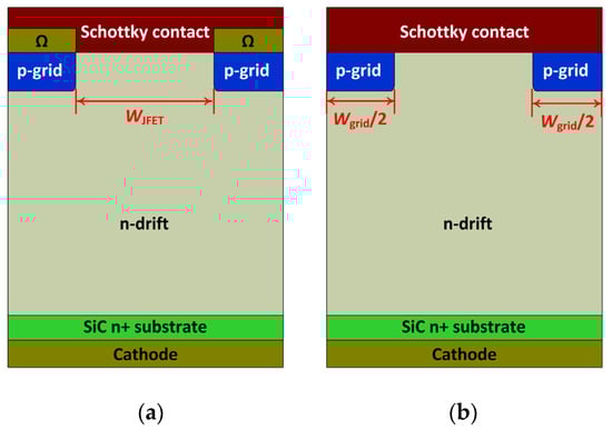
Figure 1.
Schematic structures of (a) the SiC junction barrier Schottky (JBS) diode with Ohmic contacts to the p-grids and (b) the SiC JBS diode with Schottky contacts to the p-grids.

Table 1.
Key device parameters in the studied SiC JBS diodes.
The static I-V characteristics of the SiC JBS diodes are plotted in Figure 2. The property of the contact to the p-grid in the SiC JBS diode (whether it is an Ohmic contact or a Schottky contact) does not affect the static I-V characteristics. In the forward conduction, the current mainly flows through the metal/n-drift Schottky contact, while the PN junction does not participate in the forward conduction in normal operation condition. The forward voltage drops (VF, defined at 200 A/cm2 in this paper) of the two JBS diodes are both 1.1 V. With a sufficiently high voltage applied to the JBS diode with an Ohmic contact to the p-grid, the PN junctions between p-grids and n-drift region would be turned on and contribute to the forward conduction (not shown). When the SiC material contains basal plane dislocations, the bipolar conduction through the PN junction would lead to bipolar degradation, as manifested by a shift in VF and an increase in reverse leakage current [13,14]. For the JBS diode with Schottky contact to the p-grid, the bipolar conduction through the PN junction is suppressed by the reversely biased metal/p-grid Schottky junction even at a very high forward voltage drop [10,16].
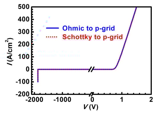
Figure 2.
Static I-V characteristics of the SiC JBS diodes.
The breakdown voltage of the JBS diodes is not affected by the property of the contact to p-grid, either. For the JBS diode with Schottky contact to p-grid, the metal/p-grid Schottky junction is forwardly biased, and the p-grid is virtually shorted to the anode in this condition. Thus, for both the two JBS diodes, the PN junctions between p-grids and n-drift region are reversely biased to support the high off-state voltage.
3. Switching Performances
In real applications, the power devices are usually operated in switching mode. Therefore, the switching performances of the studied SiC JBS diodes are critical. In this paper, the test circuit in Figure 3a is adopted to study the switching properties of the SiC JBS diodes [23,24]. The studied SiC JBS diode is the device under test (DUT). The area of the studied SiC JBS diode is 1 cm2. A stray inductance of 10 nH is assumed in the loop. A MOSFET is used as the switch for the circuit. The supply voltage is 800 V and the load current is 200 A. When the MOSFET in the circuit is turned-on, the current of the MOSFET increases to 200 A. Then, when the MOSFET is turned-off, the current of the MOSFET decreases and the current of the DUT increases because the current of the inductor L is not changed. In this period, the turning-on transient of the DUT can be studied. After the DUT is fully turned-on and works for a while, the DUT current will decrease when the MOSFET is turned-on again. Hence, the turning-off transient of the DUT can be studied when the MOSFET is turned-on.
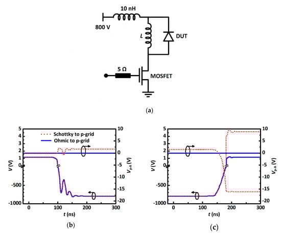
Figure 3.
(a) The circuit used to test the switching characteristics of the SiC JBS diodes. A SiC MOSFET is used as the switch. The driving signal is switched between −5 and +15 V to set the MOSFET to off- and on-state, respectively. (b) The turn-off transient of the SiC JBS diode by switching on the MOSFET (the moment when the driving signal is switched to +15 V is marked as t = 0 ns). (c) The turn-on transient of the SiC JBS diode by switching off the MOSFET (the moment when the driving signal is switched to −5 V is marked as t = 0 ns.
Figure 3b shows the turn-off transient of the SiC JBS diodes. The MOSFET is turned on at t = 0 ns. Thus, the diodes are turned off and start to sustain the 800-V reverse voltage. For the SiC JBS diode with Ohmic contact to p-grid, the high reverse voltage is biased on the internal PN junction. For the SiC JBS diode with Schottky contact to p-grid, the p-grid to anode voltage (Vp-A, defined as the voltage difference between p-grid and the anode) is clamped to ~1.7 V, near the turn-on voltage of the Schottky diode. Therefore, the off-state voltage is sustained by the PN junction inside the SiC JBS diodes, irrespective of the property of the contact to the p-grid.
When the SiC MOSFET is turned off, the SiC JBS diode is rendered into on-state, as shown in Figure 3c. The voltage across the PN junction inside the SiC JBS diode quickly drops, and then stabilizes at a forward voltage. The forward voltage of the JBS diode with an Ohmic contact to p-grid recovers to near its static value, 1.1 V. However, as to the JBS diode with a Schottky contact to p-grid, the forward voltage is almost 5 V, which is much larger than the static forward voltage shown in Figure 2. The static forward voltages of both the JBS diodes are only 1.1 V in Figure 2.
From Figure 3c, it is found the p-grid to anode voltage Vp-A is highly negative (~−17 V) after about 180 ns in the JBS diode with a Schottky contact to p-grid, which is very different to the JBS diode with Ohmic contact to p-grid where the Vp-A is 0. This phenomenon helps to explain the higher forward voltage V of almost 5 V in the JBS diode with a Schottky contact to p-grid, as the negative Vp-A of about −17 V suggests widened depletion region into n-drift region around the p-grid.
To confirm the above observed dynamic behavior of the studied SiC JBS diodes, Figure 4 shows the I-V characteristics of the JBS diodes before and after an 800-V reverse bias stress. For the JBS diode with an Ohmic contact to p-grid, the I-V characteristics after the 800-V stress are nearly the same as the initial fresh state. However, for the JBS diode with Schottky contact to p-grid, the I-V characteristic after an 800-V stress is severely degraded. The results in Figure 4 agree with the switching performance in Figure 3, confirming a degradation of dynamic VF in the SiC JBS diode with a Schottky contact to p-grid.
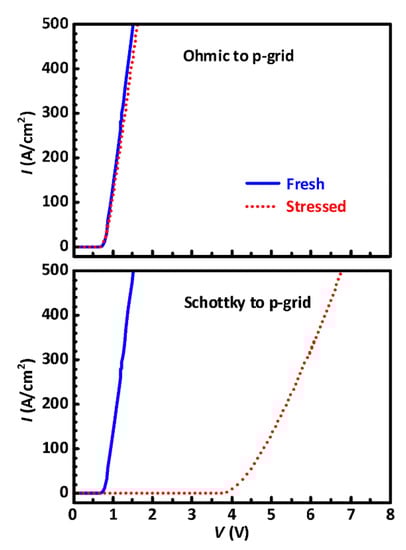
Figure 4.
The I-V characteristics under initial and stressed states of the SiC JBS diode with Ohmic contact to the p-grids and that with Schottky contact to the p-grids.
Figure 5 reveals the physical mechanism of the observed dynamic behaviors in the SiC JBS diode with a Schottky contact to p-grid. Figure 5a shows the waveform of the voltage on the SiC JBS diode with a Schottky contact to p-grid for the dynamic simulations. Figure 5b shows the electron distribution inside the SiC JBS diode with a Schottky contact to p-grids. In the initial equilibrium state, there is only a narrow depletion region around the p-grid and under the anode metal. The device is then stressed with a reverse bias of 800 V. As shown in the stressing state of the SiC JBS diode with a Schottky contact to p-grids, the n-drift region in the device is depleted to support the reverse bias. In the reverse biased state, the n-drift region is depleted to form a positive space charge region to support the high voltage, and there must be equal negative charges to pair the positive charges in the depleted n-drift region. These negative charges are located partially in the anode metal, and partially in the p-grid. Then, in the stressed state of the SiC JBS diode with a Schottky contact to p-grids, the device returns to zero biased state. The p-grid cannot be effectively discharged since the discharging current path is blocked by the reversely biased metal/p-grid Schottky junction. The p-grid becomes virtually a floating region [25,26]. Therefore, the negative charges are stored in the p-grid. To keep an equilibrium state, the depletion region around p-grid is widened for more positive charges. As the n-drift region between p-grids is depleted, the forward voltage under stressed state has to be much larger than the forward voltage in initial state to keep the same forward current. This explains the above different forward I-V characteristics before and after stress.
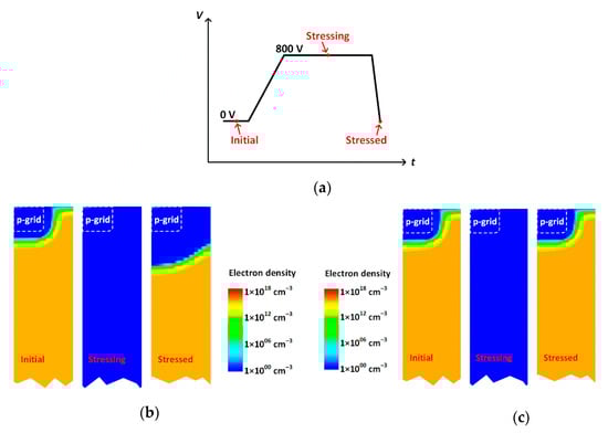
Figure 5.
(a) Waveform of the voltage on the SiC JBS diode with a Schottky contact to p-grid for dynamic simulations. The electron distribution in the SiC JBS diodes with (b) Schottky contact to p-grids and (c) Ohmic contact to p-grids. The time used to turn the device from the stressing state to stressed state under 0 V is 1 µs.
Figure 5c displays the electron distribution inside the SiC JBS diode with an Ohmic contact to p-grids for comparison. The initial and stressed states have the same electron distribution, which is different to that in Figure 5b. This verifies charge storage effect does not exist in the SiC JBS diode with an Ohmic contact to p-grids.
Figure 6 uses an equivalent circuit model to illustrate the charges storage mechanism in the p-grid of the SiC JBS diode with Schottky contact to p-grid. The diode terminal capacitance consists of metal/n-drift capacitance Cm and p-grid/n-drift capacitance Cp. In additional, the Schottky contact and p-grid constitute a Schottky diode Dp. When the JBS diode is rendered to reversely biased state, Dp is forwardly biased, and thus, both Cm and Cp can be effectively charged. The amount of charges built up across Cp is:
where the capacitance Cp is [27]:
where V is the voltage applied on JBS diode, εs is dielectric constant of SiC, WD is the depletion width of p-grid and n-drift junction, Vbi is the built-in potential, and N is the doping density of n-drift region.
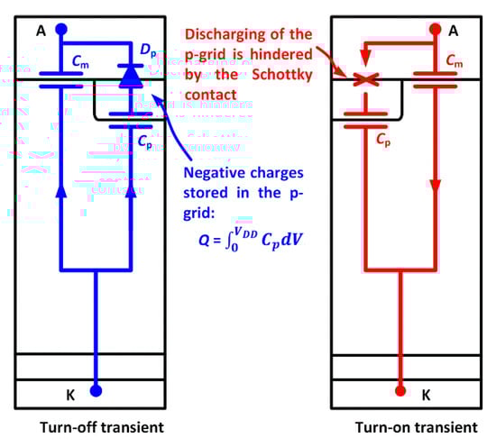
Figure 6.
Illustration of the charge storing mechanism in the SiC JBS diode with Schottky contact to p-grid.
The negative portion of the charges is located inside the p-grid. When the JBS diode is turned to forward state, Dp blocks the discharging current from the anode of the JBS diode to Cp. Therefore, the negative charges are stored in the p-grid (i.e., the node between Cp and Dp in the equivalent circuit).
The difference between the initial VF (VF-init) and the stressed VF (VF-stre) of the SiC JBS diode with Schottky contact to p-grid is influenced by the WJFET. As shown in Figure 7, when WJFET is larger, both VF-init and VF-stre become smaller, and their difference is reduced. Theoretically, when WJFET is much larger than the depletion region around the p-grid, the VF-stre would become the same as VF-init. However, with a large WJFET, the screening effect of the p-grid becomes weak, which results in a higher electric filed at the Schottky contact (EJ) when sustaining the high off-state voltage. This means that a large WJFET makes the JBS diode more Schottky barrier diode (SBD)-like [28,29]. The large EJ is undesirable regarding leakage current and reliability [30]. The trade-off between Schottky junction field EJ (at the middle of Schottky contact between p-grids) in off-state and the VF of the SiC JBS diode with Schottky contact to p-grid is shown in Figure 7. The figure indicates that increasing the WJFET cannot eliminate the dynamic dispersion of VF. Therefore, an Ohmic contact to p-grid is required in SiC JBS diode.
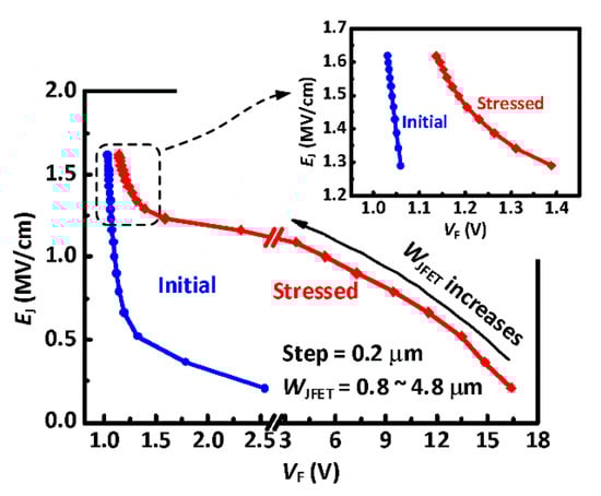
Figure 7.
The trade-off between Schottky junction field EJ and the forward voltage VF in SiC JBS with a Schottky contact to p-grid.
4. Conclusions
This work reveals the significance of the property of electrical contact to p-grid in power devices. The silicon carbide (SiC) junction barrier Schottky (JBS) diode, which is widely used in power circuits, is adopted in this paper as a case study. The property of the contact to p-grid (whether it is a Schottky contact or an Ohmic contact) does not affect the static characteristics of the JBS diodes; however, the dynamic forward voltage drop (VF) of the JBS diode with a Schottky contact to p-grid is enlarged. This phenomenon is explained by the charge storage in the p-grid. The rectifying Schottky contact allows the charging of p-grid in reverse bias state, but it hinders the discharging of p-grid after the JBS diode returns to forward state. Thus, negative charges remain in the p-grid, decreasing the potential of the p-grid, depleting the n-drift region around the p-grid, and leading to an increased VF during switching operation. An Ohmic contact to the p-grid is essential for eliminating the dynamic dispersion in the power device. Therefore, an Ohmic contact to p-grid is essential in power devices.
Author Contributions
Conceptualization, M.Z. and J.W.; software, M.Z. and M.H.; investigation, M.Z. and M.H.; writing—original draft preparation, M.Z.; writing—review and editing, B.L. and J.W.; supervision, B.L.; project administration, B.L. All authors have read and agreed to the published version of the manuscript.
Funding
This research was supported by the National Natural Science Foundation of China under Grant 51907127 and Grant 61604098, by the High-level University Fund under Grant G02236002 and Grant G02236005, by the Shenzhen Science and Technology Innovation Commission under Grant JCYJ20170412110137562, and also by the Shenzhen University Scientific Research Start-up Foundation under Grant 860-000002110207.
Conflicts of Interest
The authors declare no conflict of interest.
References
- Baliga, B.J. Fundamentals of Power Semiconductor Device; Springer: New York, NY, USA, 2008. [Google Scholar]
- Jiang, H.; Wei, J.; Dai, X.; Ke, M.; Deviny, I.; Mawby, P. SiC trench MOSFET with shielded fin-shaped gate to reduce oxide field and switching loss. IEEE Electron Device Lett. 2016, 37, 1324–1327. [Google Scholar] [CrossRef]
- Chung, G.Y.; Tin, C.C.; Williams, J.R.; McDonald, K.; Chanana, R.K.; Weller, R.A.; Pantelides, S.T.; Feldman, L.C.; Holland, O.W.; Das, M.K.; et al. Improved inversion channel mobility for 4H-SiC MOSFETs following high temperature anneals in nitric oxide. IEEE Electron Device Lett. 2001, 22, 176–178. [Google Scholar] [CrossRef]
- Yano, H.; Hirao, T.; Kimoto, T.; Matsunami, H.; Asano, K.; Sugawara, Y. High channel mobility in inversion layers of 4H-SiC MOSFET’s by utilizing (11-20) face. IEEE Electron Device Lett. 1999, 20, 611–613. [Google Scholar] [CrossRef]
- Harada, S.; Kato, M.; Kojima, T.; Ariyoshi, K.; Tanaka, Y.; Okumura, H. Determination of optimum structure of 4H-SiC trench MOSFET. In Proceedings of the 2012 International Symposium on Power Semiconductor Devices and ICs (ISPSD), Bruges, Belgium, 3–7 June 2012; pp. 253–256. [Google Scholar]
- Peters, D.; Siemieniec, R.; Aichinger, T.; Basler, T. Performance and ruggedness of 1200V SiC—Trench—MOSFET. In Proceedings of the 2017 International Symposium on Power Semiconductor Devices and ICs (ISPSD), Sapporo, Japan, 28 May–1 June 2017; pp. 239–242. [Google Scholar]
- Pala, V.; Barkley, A.; Hull, B.; Wang, G.; Ryu, S.; Van Brunt, E.; Lichtenwalner, D.; Richmond, J.; Jonas, C.; Capell, C.; et al. 900 V silicon carbide MOSFETs for breakthrough power supply design. In Proceedings of the 2015 IEEE Energy Conversion Congress and Exposition (ECCE), Montreal, QC, Canada, 20–24 September 2015; pp. 4145–4150. [Google Scholar]
- Jiang, M.; Shen, Z.J. Simulation study of an injection enhanced insulated-gate bipolar transistor with p-base schottky contact. IEEE Trans. Electron Devices 2016, 63, 1991–1995. [Google Scholar] [CrossRef]
- Wu, T.; Bakeroot, B.; Liang, H.; Posthuma, N.; You, S.; Ronchi, N.; Stoffels, S.; Marcon, D.; Decoutere, S. Analysis of the gate capacitance-voltage characteristics in p-GaN/AlGaN/GaN heterostructures. IEEE Electron Device Lett. 2017, 38, 1696–1699. [Google Scholar] [CrossRef]
- Tallarico, A.N.; Stoffels, S.; Magnone, P.; Posthuma, N.; Sangiorgi, E.; Decoutere, S.; Fiegna, C. Investigation of the p-GaN gate breakdown in forward-biased GaN-based power HEMTs. IEEE Electron Device Lett. 2017, 38, 99–102. [Google Scholar] [CrossRef]
- Injun, H.; Jongseob, K.; Hyuk, S.C.; Hyoji, C.; Jaewon, L.; Kyung, Y.K.; Jong-Bong, P.; Jae, C.L.; Jongbong, H.; Jaejoon, O.; et al. p-GaN gate HEMTs with tungsten gate metal for high threshold voltage and low gate current. IEEE Electron Device Lett. 2013, 34, 202–204. [Google Scholar]
- Lee, F.; Su, L.; Wang, C.; Wu, Y.; Huang, J. Impact of gate metal on the performance of p-GaN/AlGaN/GaN high electron mobility transistors. IEEE Electron Device Lett. 2015, 36, 232–234. [Google Scholar] [CrossRef]
- Fayyaz, A.; Romano, G.; Castellazzi, A. Body diode reliability investigation of SiC power MOSFETs. Microelectron. Reliab. 2016, 64, 530–534. [Google Scholar] [CrossRef]
- Ebihara, Y.; Uehara, J.; Ichimura, A.; Mitani, S.; Noborio, M.; Takeuchi, Y.; Tsuruta, K. Suppression of bipolar degradation in deep-p encapsulated 4H-SiC trench MOSFETs up to ultra-high current density. In Proceedings of the 2019 International Symposium on Power Semiconductor Devices and ICs (ISPSD), Shanghai, China, 19–23 May 2019; pp. 35–38. [Google Scholar]
- Agarwal, A.; Haney, S. Some critical materials and processing issues in SiC power devices. J. Electron. Mater. 2008, 37, 646–654. [Google Scholar] [CrossRef]
- Fengping, C.; Yuming, Z.; Hongliang, L.; Yimen, Z.; Hui, G.; Xin, G. Fabrication and characteristics of a 4H-SiC junction barrier Schottky diode. J. Semicond. 2011, 32, 64003. [Google Scholar]
- Nishio, J.; Ota, C.; Hatakeyama, T.; Shinohe, T.; Kojima, K.; Nishizawa, S.; Ohashi, H. Ultralow-loss SiC floating junction Schottky barrier diodes (super-SBDs). IEEE Trans. Electron Devices 2008, 55, 1954–1960. [Google Scholar] [CrossRef]
- Cooper, J.A.; Agarwal, A. SiC power-switching devices—The second electronics revolution? Proc. IEEE 2002, 90, 956–968. [Google Scholar] [CrossRef]
- Zhang, M.; Wei, J.; Jiang, H.; Chen, K.J.; Cheng, C. A new SiC trench MOSFET structure with protruded p-base for low oxide field and enhanced switching performance. IEEE Trans. Device Mater. Reliab. 2017, 17, 432–437. [Google Scholar] [CrossRef]
- Han, K.; Baliga, B.J.; Sung, W. Split-gate 1.2-kV 4H-SiC MOSFET: Analysis and experimental validation. IEEE Electron Device Lett. 2017, 38, 1437–1440. [Google Scholar] [CrossRef]
- Kimoto, T.; Niwa, H.; Kaji, N.; Kobayashi, T.; Zhao, Y.; Mori, S.; Aketa, M. Progress and future challenges of SiC power devices and process technology. In Proceedings of the 2017 IEEE International Electron Devices Meeting (IEDM), 2–6 December 2017; pp. 227–230. [Google Scholar]
- Wei, J.; Jiang, H.; Jiang, Q.; Chen, K.J. Proposal of a GaN/SiC hybrid field-effect transistor for power switching applications. IEEE Trans. Electron Devices 2016, 63, 2469–2473. [Google Scholar] [CrossRef]
- Wei, J.; Zhang, M.; Jiang, H.; Cheng, C.; Chen, K.J. Low ON-resistance SiC trench/planar MOSFET with reduced OFF-state oxide field and low gate charges. IEEE Electron Device Lett. 2016, 37, 1458–1461. [Google Scholar] [CrossRef]
- Linder, S. Power Semiconductors; EPFL Press: Lausanne, Switzerland, 2006. [Google Scholar]
- Takaya, H.; Miyagi, K.; Hamada, K. Floating islands and thick bottom oxide trench gate MOSFET (FITMOS) with passive hole gate −60V ultra low on-resistance novel MOSFET. In Proceedings of the 2006 International Electron Devices Meeting (IEDM), San Francisco, CA, USA, 11–13 December 2006; pp. 1–4. [Google Scholar]
- Wei, J.; Zhang, M.; Jiang, H.; Wang, H.; Chen, K.J. Dynamic degradation in SiC trench MOSFET with a floating p-shield revealed with numerical simulations. IEEE Trans. Electron Devices 2017, 64, 2592–2598. [Google Scholar] [CrossRef]
- Sze, S.M. Physics of Semiconductor Devices, 3rd ed.; John Wiley & Sons Inc.: Hoboken, NJ, USA, 2006. [Google Scholar]
- Ren, N.; Wang, J.; Sheng, K. Design and experimental study of 4H-SiC trenched junction barrier Schottky diodes. IEEE Trans. Electron Devices 2014, 61, 2459–2465. [Google Scholar] [CrossRef]
- Di Benedetto, L.; Licciardo, G.D.; Erlbacher, T.; Bauer, A.J.; Bellone, S. Analytical model and design of 4H-SiC planar and trenched JBS diodes. IEEE Trans. Electron Devices 2016, 63, 2474–2481. [Google Scholar] [CrossRef]
- Jiang, H.; Wei, J.; Dai, X.; Zheng, C.; Ke, M.; Deng, X.; Sharma, Y.K.; Deviny, I.; Mayby, P. SiC MOSFET with built-in SBD for reduction of reverse recovery charge and switching loss in 10-kV applications. In Proceedings of the 2017 International Symposium on Power Semiconductor Devices and ICs (ISPSD), Sapporo, Japan, 28 May–1 June 2017; pp. 49–52. [Google Scholar]
Publisher’s Note: MDPI stays neutral with regard to jurisdictional claims in published maps and institutional affiliations. |
© 2020 by the authors. Licensee MDPI, Basel, Switzerland. This article is an open access article distributed under the terms and conditions of the Creative Commons Attribution (CC BY) license (http://creativecommons.org/licenses/by/4.0/).