Abstract
An enhancement-mode gallium-nitride high-electron-mobility transistor (E-mode GaN HEMT) operated at high frequency is highly prone to current spikes (di/dt) and voltage spikes (dv/dt) in the parasitic inductor of its circuit, resulting in damage to the power switch. To highlight the phenomena of di/dt and dv/dt, this study connected the drain, source, and gate terminals in series with inductors (LD, LS, and LG, respectively). The objective was to explore the effects of di/dt and dv/dt phenomena and operating frequency (fS) on drain-to-source voltage (Vds), drain-to-source current (Ids), and gate-to-source voltage (Vgs). The experimental method comprised two projects: (1) establishment of a measurement system to assess the change of electrical characteristics of the E-mode GaN HEMT and (2) change of the fS and the inductances (i.e., LD, LS, and LG) in the circuit to measure the changes in Vds, Ids, and Vgs, thus summarizing the experimental results. According to the experimental results on electrical characteristics, a gate driver circuit may be designed to drive and protect the E-mode GaN HEMT while being actually applied to a 120-W synchronous buck converter with an output voltage of 12 V and an output current of 10 A.
1. Introduction
The gradual yearly increase of greenhouse gases has intensified global warming. Energy-saving and carbon reduction have become the primary development goals for each country. The demand for relevant regulations (e.g., the Energy Star Standard and California Energy Commission Appliance Efficiency Regulations) and the market in recent years have driven the continual development of high-efficiency and high-power-intensity power supply units [1,2]. Because wide-bandgap materials are characterized by high breakdown voltage and high electron mobility, which merit operation under high temperatures and high frequencies [3,4,5,6,7,8,9,10], they have enabled the development of power supply units to gradually transition from silicon power switches to wide-bandgap power switches [3,4,5].
Wide-bandgap semiconductors may be categorized by their internal structures into enhancement-mode gallium-nitride high-electron-mobility transistors (E-mode GaN HEMTs) and gallium-nitride high-electron-mobility transistors (GaN HEMTs) [11]. Table 1 presents a comparison between key parameters (static, dynamic, and reverse operation) of E-mode GaN HEMT and GaN HEMT. The following findings were revealed from the comparison: (1) regarding static parameters, E-mode GaN HEMT with a RDS(ON) value smaller than that of GaN HEMT yielded lower conduction loss. (2) Regarding dynamic parameters, both transistors are voltage-driven components that require charging and discharging of a parasitic inductor between gate-to-source and gate-to-drain terminals for conduction and cut-off. That is, because the total gate charge (QG), gate–source charge (QGS), and gate–drain charge (QGD) of E-mode GaN HEMT were lower than those of GaN HEMT, E-mode GaN HEMT required less time for conduction and cut-off as well as experienced weaker di/dt and dv/dt. (3) Reverse-recovery charge (QRR) of the E-mode GaN HEMT was approximately zero under reverse operation, constituting an extremely short reverse recovery time as well as minimal component loss and electromagnetic interference. Given the three aforementioned advantages of E-mode GaN HEMT, this study employed it for the experiment.

Table 1.
The key parameters compare the enhancement-mode gallium-nitride high-electron-mobility transistors (E-mode GaN HEMTs) with the GaN HEMT [12,13].
High-frequency operation subjects the parasitic inductor of the circuit to di/dt and dv/dt phenomena, which could entail oscillation in voltage and current waveforms and create electromagnetic interference. Serious electromagnetic interference can result in damage to the power switch [14].
A measurement system was first established to assess the electrical characteristics of the E-mode GaN HEMT. Subsequently, to accentuate the di/dt and dv/dt phenomena, this study connected the drain, source, and gate terminals in series with inductors (LD, LS, and LG, respectively) and adjusted inductor values before measuring the waveform changes of Vds, Ids, and Vgs. In addition, this study adjusted the operating frequency from 100 kHz to 2 MHz to measure the waveform changes of Vds and Vgs. Based on the results from the electrical characteristic experiment, this study’s aim was to design a gate driver circuit to drive the E-mode GaN HEMT while further protecting said transistor by monitoring the changes in Vgs and Ids values.
2. Measuring System
When E-mode GaN HEMT is switched on or off, di/dt and dv/dt phenomena occur. Therefore, at various operating frequencies, load currents, and inductances, a measurement system was used to assess and record the changes in Vds, Ids, and Vgs. Figure 1 presents the measurement system, composed of a function generator (fabricant: SIGLENT, model: SDG2042X), a passive circuit, a digital oscilloscope (fabricant: LECROY, model: HDO4034A), a DC power supply (fabricant: GWINSTEK, model: SPD-3606), and an E-mode GaN HEMT (the testing component; fabricant: GaN system, model:GS61004B). The experimental parameters in Figure 1 are detailed in Table 2.
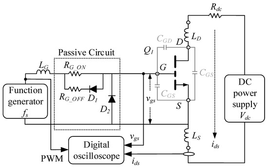
Figure 1.
The proposed measurement system to assess electrical characteristics of enhancement-mode gallium-nitride high-electron-mobility transistors (E-mode GaN HEMT).
Table 2.
Experimental parameters of Figure 1.
3. Electrical Characteristics of E-mode GaN HEMT when di/dt and dv/dt Occur
Regarding Figure 2, the GS61004B component provided by GaN Systems was loaded into TINA-TI; after a circuit diagram (Figure 2) was plotted, the Vds, Ids, and Vgs waveforms can be simulated. The simulation was performed in the condition of Ids = 2 A and fs = 150 kHz with the inductance parameters of LG = 100 nH, LD = 50 nH, and LS = 50 nH. The obtained waveforms of ID(Ids), Vds, and Vgs from the simulation are presented in Figure 3. To elucidate the exact time when di/dt and dv/dt occurred in the waveform, the maximum and minimum values of Ids were marked as Ids,max and Ids,min, respectively; the maximum and minimum values of Vds were denoted by Vds,max and Vds,min, respectively; and the maximum and minimum values of Vgs were marked as Vgs,max and Vgs,min, respectively. Subsequent experiments were implemented and recorded according to the aforementioned rules.
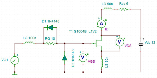
Figure 2.
Circuit simulation in TINA-TI.
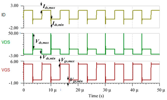
Figure 3.
Simulation of waveform changes in Ids, Vds, and Vgs when di/dt and dv/dt occur.
The parameters presented in Figure 2, namely output current, operating frequency (fs), and inductors in series (i.e., LD, LS, and LG), were changed. In four testing conditions, the maximum and minimum values of Vds, Ids, and Vgs were measured and recorded to determine spike changes.
3.1. Applying Various LD Values to Measure the Changes in Ids and Vds when di/dt and dv/dt Occur
The parameter setting of LG = LS = 1 nH, fs = 100 kHz, Vgs = 5 V, and LD = 0.01–0.50 μH was applied. Figure 4a shows that under different Ids (ranging from 0.1 A to 2.0 A) and before LD achieved 0.1 μH, the Vds,max changes of the five curves exhibited a linear relationship. After LD exceeded 0.1 μH, Vds,max underwent a rapid change, where the Vds,max value of the blue and yellow curves approximated the specification of GS61004B (Vds,max = 100 V); at that point, the experiment was terminated to avoid damaging the power switch. As presented in Figure 2, because the drain- and source-end of the GS61004B exhibited parasitic capacitance (Cds), an RLC series network was formed with the loops of Vdc, Rdc, LD, Cds, and LS. Therefore, with the circuit parameters Rdc = 6 Ω, LS = 1 nH, LD = 0.05–0.30 µH, and Cds = 105 pF [16], the damping ratio (ζ) [17] was calculated to be 0.137, 0.125, 0.116, 0.109, 0.102, 0.097, 0.069, and 0.056. The curve of Ids = 2 A in Figure 4a illustrates the relationship between LD and Vds,max. When ζ = 0.137 (LD = 0.05 µH), the Vds,max amplitude was low, whereas it was high when ζ = 0.056 (LD = 0.30 µH).
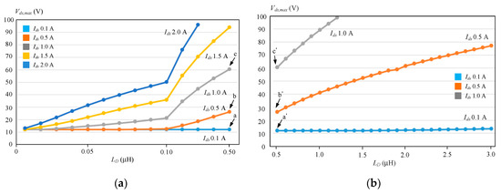
Figure 4.
Changes in Vds when different Ids values are applied. (a) Changes in Vds,max for various Ids values (LD ranges from 0.01–0.50 μH). (b) Changes in Vds,max for various Ids values (LD ranges from 0.5–3.0 μH).
Subsequently, the Vds,max values of corresponding Points a (12.01 V), b (26.26 V), and c (60.49 V) on the gray, orange, and light blue curves, respectively, were found to not reach 100 V. Therefore, the researcher could continue to increase the LD for the three curves. In Figure 4b, LD ranges from 0.5 μH to 3.0 μH and Points a′, b′, and c′ correspond to points a, b, and c in Figure 4a. The researcher continued to increase LD until the gray curve first yielded Vds,max = 98 V; the experiment for the gray curve was terminated. Subsequently, when the LD was increased to 3.0 μH, the orange and the light blue curves yielded Vds,max values of 77.19 V and 13.46 V, respectively, both of which are lower than Vds,max = 100 V.
3.2. Applying Different LG Values to Measure the Changes of Vds and Vgs When di/dt and dv/dt Occur
The parameter setting of Ids = 2 A, LS = 1 nH, fs = 100 kHz, Vgs = 5 V, and LG = 0.001–0.500 μH was applied. In Figure 5a, orange (Vds,min,a) and gray curves (Vds,max,a) are used for when LD = 0.2 μH and blue (Vds,min,b) and yellow curves (Vds,max,b) for LD = 1.0 nH to observe Vds changes. A comparison of Vds,min,a and Vds,min,b values when LG was changed from 0.001 μH to 0.5 μH revealed that Vds,min,b was still approximately zero, whereas Vds,min,a ranged from −1.33 V to −1.40 V. Because the drain terminal of the GS61004B was connected to LD = 1 nH, the inductance was relatively low, with Vds,max,b remaining at approximately 12 V; almost no change was observed. By contrast, when LD = 0.2 μH, the inductance increased, with Vds,max,a ranging between 72 V and 76 V. This shows that connecting the drain terminal of GS61004B to an inductor with excessively large inductance causes an increase in Vds,max and Vds,min.
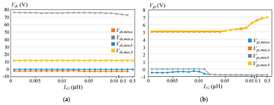
Figure 5.
Changes in Vds and Vgs for different LG values. (a) Changes in Vds,max and Vds,min for different LG values. (b) Changes in Vgs,max and Vgs,min for different LG values.
The blue (Vgs,min,a) and red curves (Vgs,max,a) are used for when LD = 0.2 μH, and the gray (Vds,min,b) and yellow curves (Vds,max,b) are used when LD = 1.0 nH to observe changes of Vgs, as shown in Figure 5b. Before LG reached 0.01 μH, Vgs,min,a ranged from −0.34 V to −0.49 V, but rose to −0.64–−0.81 V after LG reached 0.01 μH. Vgs,min,b remained almost 0 before LG reached 0.02 μH, but the range of Vgs,min,b rose to −0.73–−0.80 V after LG reached 0.02 μH. When LD was set to 0.2 μH, Vgs,max,a ranged from 5.00 V to 6.85 V; when LD was set to 1.0 nH, Vds,max,b ranged from 5.10 V to 6.97 V. Neither voltage value exceeded the specifications for GS61004B (Vgs,max = 7 V). Because the drain terminal of GS61004B was connected to LD, no direct effect was exerted on Vgs,max and Vgs,min. The gate terminal of GS61004B was connected to LG, which caused Vgs,max and Vgs,min to increase with the value of LG.
3.3. Applying Different LS Values to Measure the Changes of Ids, Vds, and Vgs When di/dt and dv/dt Occur
The parameter setting of Ids = 2 A, LG = 1 nH, fs = 100 kHz, Vgs = 5 V, and LS = 0.001–2.000 μH was applied. The blue curve (Ids,min,a) is used when LD = 0.2 μH and the orange curve (Ids,min,b) is used when LD = 1.0 nH to observe changes of Ids. In Figure 6a, Ids,min,a ranges from −1.40 A to −1.84 A, whereas the changes of Ids,min,b are divided into three sections detailed as follows. In the first section, where LS ranged from 0.001 to 0.010 μH, Ids,min,b was approximately 0 A; in the second section, where LS ranged from 0.01 μH to 0.1 μH, Ids,min,b was between −0.11 A and −1.13 A; and in the third section, where LS ranged from 0.1 μH to 2.0 μH, Ids,min,b was between −1.13 A and −1.83 A. As shown in Figure 6a, when Ls = 0.01 μH and 1.00 μH, Ids,min decreased sharply. Theses phenomena are elucidated as follows: As indicated by the blue curve, in the Ids loop, the inductance value for the series connection of LD = 0.20 μH and LS = 0.01 μH was LDS(blue) = 0.21 μH, and Ids,min = −1.4 A; when LD = 0.20 μH and LS = 1.00 μH, LDS(blue) = 1.20 μH and Ids,min = −1.69 A. The inductance increased by 5.7 times from 0.21 μH to 1.20 μH, indicating a significant change in Ids,min. As depicted by the orange curve, the inductance value for the series connection of LD = 1 nH (0.001 μH) and LS = 0.01 μH was LDS(orange) = 0.011 μH, and Ids,min = −0.1 A; when LD = 1 nH (0.001 μH) and LS = 1.00 μH, LDS(orange) = 1.001 μH, and Ids,min = −1.7 A. The inductance increased 91 times from 0.011 μH to 1.001 μH, indicating that the change in the Ids,min was larger for the orange curve than for the blue curve.
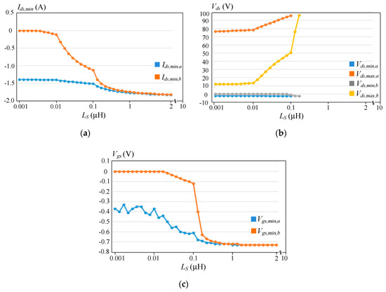
Figure 6.
Changes in Ids, Vds, and Vgs when different LS are applied. (a) Changes in Ids for different LS. (b) Changes in Vds for different LS. (c) Changes in Vgs for different LS.
In Figure 6b, the blue (Vds,min,a) and orange curves (Vds,max,a) are used when LD = 0.2 μH and the gray and yellow curves are used when LD = 1.0 nH to observe changes in Vds. In the section where LS was between 0.001 μH and 0.01 μH, Vds,min,a ranged between −2.16 V and −2.49 V, whereas Vds,max,a ranged between 76.47 V and 78.38 V. After LS reached 0.01 μH, Vds,min,a did not exhibit much variation, but Vds,max,a rose considerably to 80.57–95.88 V. The value of Vds,min,b approximated 0 until LS reached 0.1 μH, which was when Vds,min,b decreased from 0 to −2.50 V. Changes in Vds,max,b may be divided into three sections: When LS = 0.001–0.010 μH, 0.01–0.10 μH, and 0.1–0.3 μH, the corresponding ranges of Vds,max,b were 12.01–13.15 V, 13.51–50.42 V, and 50.42–96.19 V, respectively. Because in the third section, Vds,max,b was approximating 100 V, the subsequent experiment was terminated. According to the aforementioned experimental results, reducing LD to 1 nH, maintaining LS in the loop of Ids, gradually increasing LS caused Ids,max, Ids,min, Vds,max, and Vds,min to rise.
In Figure 6c, the blue curve (Vgs,min,a) is used when LD = 0.2 μH, and the orange curve (Vgs,min,b) is used when LD = 1.0 nH to observe changes of Vgs. Vgs,min,a began at −0.4 V and continued to drop until LS reached 0.2 μH, after which it gradually stabilized and eventually remained at approximately −0.7 V. The variation in Vgs,min,b may be divided into two sections. When LS = 0.001–0.1 μH, Vgs,min,b was −0.12–0 V, showing negligible variation. When LS = 0.2–2.0 μH, Vgs,min,b was −0.73–−0.4 V. This experiment revealed that because LS was not in the loop of Vgs, its effect on Vgs,min was limited.
3.4. Applying Different LS Values to Measure the Changes of Ids, Vds, and Vgs When di/dt and dv/dt Occur
The parameter setting of Ids = 1 A, LG = 10 nH, LD = LS = 1 nH, Vgs = 5 V, and fs = 100 kHz–2 MHz was applied. In Figure 7, the blue (Vds,max), orange (Vgs,min), and gray (Vgs,max) curves are used to observe changes in both Vds and Vgs,. Vds,max was found to remain at approximately 15 V, Vgs,min remained at approximately −0.64 V, and Vgs,max varied from 5.61 V to 6.12 V. According to the experimental results, the parasitic capacitance of E-mode GaN HEMT was extremely low. Take GS61004B as an example, Ciss = 328 pF, Coss = 133 pF, and CRss = 5 pF. This shows that the operating frequency of 100 kHz–2 MHz was suitable for GS61004B.
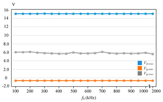
Figure 7.
Changes in Vds and Vgs when different fs values are applied.
4. Framework and Application of Gate Driver Circuit
According to the aforementioned experimental results, connecting inductors with excessively large inductance in series to the circuit loop of Vgs and Ids tends to aggravate the dv/dt and di/dt phenomena. To avoid drastic spikes in the voltage and current waveforms that may damage E-mode GaN HEMT, this study designed a gate driver circuit in the hope of protecting E-mode GaN HEMT by monitoring Vgs and Ids values. In Figure 8, the gate driver circuit comprises a controller, an isolated driver (UCC21520), a gate driver (LM5113), a high-speed amplifier (AD8028), and a shunt resistor (RS). When the pulse width modulation (PWM) signal of Vgs is switched from on to off, the controller detects the positive and negative trigger sources to ensure that Vgs does not exceed the range between +7 V and −4 V. When E-mode GaN HEMT is switched on or off, the controller detects Ids changes through the shunt resistor to ensure that Ids remains within the designated value range. When Vgs or Ids exceeds the set range, the controller turns off the gate driver to avoid damage to the E-mode GaN HEMT. In addition, the gate driving circuit is composed of three terminals: A, B, and C. Terminal A is connected to the gate terminal of the E-mode GaN HEMT, Terminal B is connected to the source terminal of the E-mode GaN HEMT, and Terminal C is connected to other components (Figure 9).
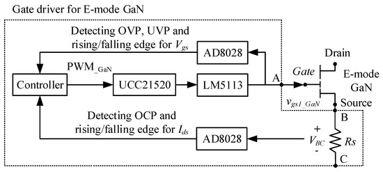
Figure 8.
Block diagram of the gate driver circuit.
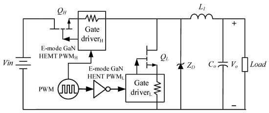
Figure 9.
Application of gate driver circuit to the synchronous buck converter.
In Figure 9, two gate driver circuits are installed to the synchronous buck converter, which is applied to a 48-V electric scooter system. Parameters applied to the synchronous buck converter are presented in Table 3. Figure 10a shows the PWM waveforms of QH and QL subject to no-load current; the green waveform shows that at a 0.18 duty cycle, the dv/dt at the negative terminal was −1.6 V. The red waveform indicates that, at a 0.77 duty cycle, the spike dv/dt at the negative terminal was −1.9 V. Figure 10b shows the PWM waveforms of QH and QL subject to a full-load current. The green waveform shows that at a 0.28 duty cycle, the dv/dt at the negative terminal was −1.6 V. The red waveform indicates that, at a 0.70 duty cycle, the dv/dt at the negative terminal was −3.6 V. Waveforms of the output voltage (Vo) and output current (Io) of the synchronous buck converter are presented in Figure 11, where Vo = 12.2 V and Io = 10.0 A, both of which meet the specifications in Table 3.
Table 3.
Experimental parameters of Figure 9.
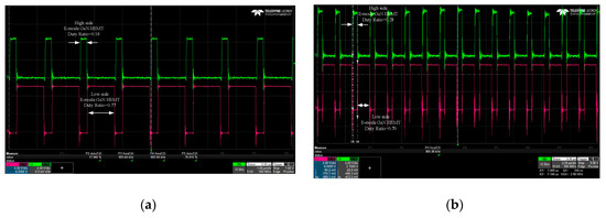
Figure 10.
PWM signals of E-mode GaN HEMT. (a) No-load, 2 V/div, time: 1 μs/div. (b) Full-load, 2 V/div, time: 1 μs/div.
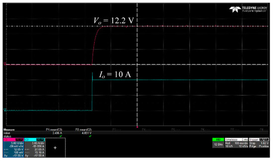
Figure 11.
Waveforms of output voltage and output current. 5 V/div, 5 A/div, time: 100 ms/div.
5. Conclusions
This study explored factors influencing the spike magnitude when di/dt and dv/dt occur to GS61004B. A gate drive circuit was designed and applied to the synchronous buck converter. The following conclusions were drawn from the experimental results.
- When the dv/dt of Vds and the di/dt of Ids are excessively large, the LD of the Ids circuit loop may first be reduced before LS is reduced.
- When the dv/dt of Vgs is excessively large, the LG of the Vgs circuit loop may first be reduced.
- When LD, LG, and LS are maintained at a minimum value, the optimal operating frequency for GS61004B is 100 kHz–2 MHz.
- The gate driver circuit is suitable for 120-W synchronous buck converter.
Funding
This research was funded by the Ministry of Science and Technology as a Project of MOST Research (No. MOST 107-2218-E-150-004-MY2).
Conflicts of Interest
The authors declare no conflict of interest.
References
- Radić, A.; Ahssanuzzaman, S.M.; Mahdavikhah, B.; Prodić, A. High-Power Density Hybrid Converter Topologies for Low-Power DC-DC SMPS. In Proceedings of the 2014 International Power Electronics Conference (IPEC-Hiroshima 2014-ECCE ASIA), Hiroshima, Japan, 18–21 May 2014; pp. 3582–3586. [Google Scholar]
- Halder, T. Power Density & Thermal Limits of the Flyback SMPS, the Flyback SMPS. In Proceedings of the 2016 IEEE First International Conference on Control, Measurement and Instrumentation (CMI), Kolkata, India, 8–10 January 2016; pp. 1–5. [Google Scholar]
- Avila, A.; Garcia-Bediaga, A.; Oñederra, O.; Ruias, A.; Rodriguez, A. Comparative Analysis of GaN HEMT vs. Si Cool MOS for a High-Frequency MMC Topology. In Proceedings of the 2017 19th European Conference on Power Electronics and Applications (EPE’17 ECCE Europe), Warsaw, Poland, 11–14 September 2017; pp. 1–9. [Google Scholar]
- Balda, J.C.; Mantooth, A. Power-semiconductor devices and components for new power converter developments. IEEE Power Electron. Mag. 2016, 3, 53–56. [Google Scholar] [CrossRef]
- Millan, J.; Godignon, P.; Perpina, X.; Perez-Tomas, A.; Rebollo, J. A survey of wide bandgap power semiconductor devices. IEEE Trans. Power Electron. 2014, 29, 2155–2163. [Google Scholar] [CrossRef]
- Ramachandran, R.; Nymand, M. Experimental demonstration of a 98.8% efficient isolated DC-DC GaN converter. IEEE Trans. Ind. Electron. 2017, 64, 9104–9113. [Google Scholar]
- Han, D.; Morris, C.T.; Lee, W.; Sarlioglu, B. A case study on common Mode electromagnetic interference characteristics of GaN HEMT and Si MOSFET power converters for EV/HEVs. IEEE Trans. Transp. Electrif. 2017, 3, 168–179. [Google Scholar] [CrossRef]
- Kaminski, N. State of the Art and the Future of Wide Band-Gap Devices. In Proceedings of the 2009 13th European Conference on Power Electronics and Applications, Barcelona, Spain, 8–10 September 2009; pp. 1–9. [Google Scholar]
- Han, D.; Noppakunkajorn, J.; Sarlioglu, B. Comprehensive efficiency, weight, and volume comparison of SiC- and Si-based bidirectional DC-DC converters for hybrid electric vehicles. IEEE Trans. Veh. Technol. 2014, 63, 3001–3010. [Google Scholar] [CrossRef]
- Biela, J.; Schweizer, M.; Waffler, S.; Kolar, J.W. SiC versus Si-evaluation of potentials for performance improvement of inverter and DC-DC converter systems by SiC power semiconductors. IEEE Trans. Ind. Electron. 2011, 58, 2872–2882. [Google Scholar]
- Lidow, A.; Strydom, J.; de Rooij, M.; Reusch, D. GaN Transistors for Efficient Power Conversion; Wiley: Hoboken, NJ, USA, 2014; pp. 1–10. [Google Scholar]
- GaN System Inc. Top Cooled 650V Enhancement Mode GaN Transistor Preliminary Datasheet (GS66508T); GaN System Inc.: Ottawa, ON, Canada, 2015. [Google Scholar]
- Transphorm Inc. AEC-Q101 Qualified 650V Cascode GaN FET in TO-247 (TPH3205WSBQA); Transphorm Inc.: Goleta, CA, USA, 2017. [Google Scholar]
- GaN System Inc. How to Drive GaN Enhancement Mode HEMT (GN001); GaN System Inc.: Ottawa, ON, Canada, 2016. [Google Scholar]
- Diodes Incorporated. 1N4148 datasheet (1N4148WS); Diodes Incorporated: Plano, TX, USA, 2016. [Google Scholar]
- GaN System Inc. 100V Enhancement Mode GaN Transistor Datasheet (GS61004B); GaN System Inc.: Ottawa, ON, Canada, 2004. [Google Scholar]
- Irwin, J.D.; Nelms, R.M. Engineering Circuit Analysis, 11th ed.; Wiley: Hoboken, NJ, USA, 2015. [Google Scholar]
© 2020 by the author. Licensee MDPI, Basel, Switzerland. This article is an open access article distributed under the terms and conditions of the Creative Commons Attribution (CC BY) license (http://creativecommons.org/licenses/by/4.0/).