1. Introduction
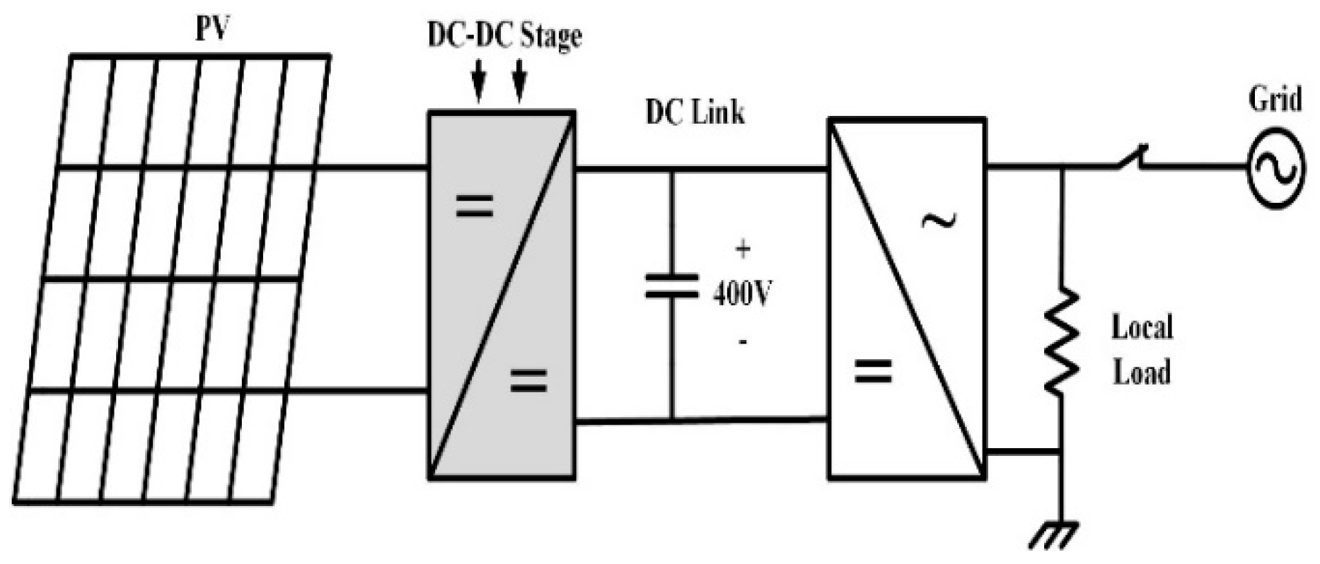
Emerging renewable energy sources, such as solar PV and fuel cells, produce a very low DC voltage. Integrating them into the grid requires a converter with high voltage gain capability such as the system in
Figure 1. The conventional boost converter cannot meet the required voltage gain unless there is a series connection for several input sources, and it also requires a galvanic isolation stage since it is not isolated.
In addition, these sources require a smooth input current to make maximal power tracking possible. To address these issues, several techniques have been proposed [
1,
2,
3]. Some non-isolated topologies were proposed in [
4,
5,
6,
7,
8,
9,
10] to provide a high voltage gain and reduce the voltage stress on switches and diodes. In [
4], the high conversion ratio was achieved through a multi-winding coupled inductor that feeds two multiplier cells. The main switch in this converter is hard switched and the input current consists of high ripple. Papers [
5,
6,
7] present converters with high voltages and low input current ripple, utilizing SEPIC based converters and integrating multiplier cells coupled to the second inductor. The main switch, however, is still hard switched and the required duty cycle for 380 V applications is still higher than 0.5. Converters from [
8,
9,
10] produce high voltage gain and reduced stress on switches but still introduce high input current ripple. Converters from [
11,
12,
13] have solved these issues by being high voltage gain with ZVS and low input ripple. These would be good candidates for an application where galvanic isolation is not required. In the case where galvanic isolation is required, high frequency isolated DC–DC converters become the viable choice. Current fed, isolated DC–DC converters are the favorite in this category due to their boosting capability and their low ripple input current; additionally, they utilize high-frequency transformers with a relatively simple structure [
14,
15,
16]. In these topologies, the duty cycle is usually more than 0.5. In [
14,
15,
16], boosting was achieved through a transformer with a turn’s ratio, and ZVS operation of the main switches was realized but the transformer’s turns ratio needed to be high for sufficient voltage gain. In addition, the high turn’s ratio will reflect on the voltage stress of the secondary side switches and diodes.
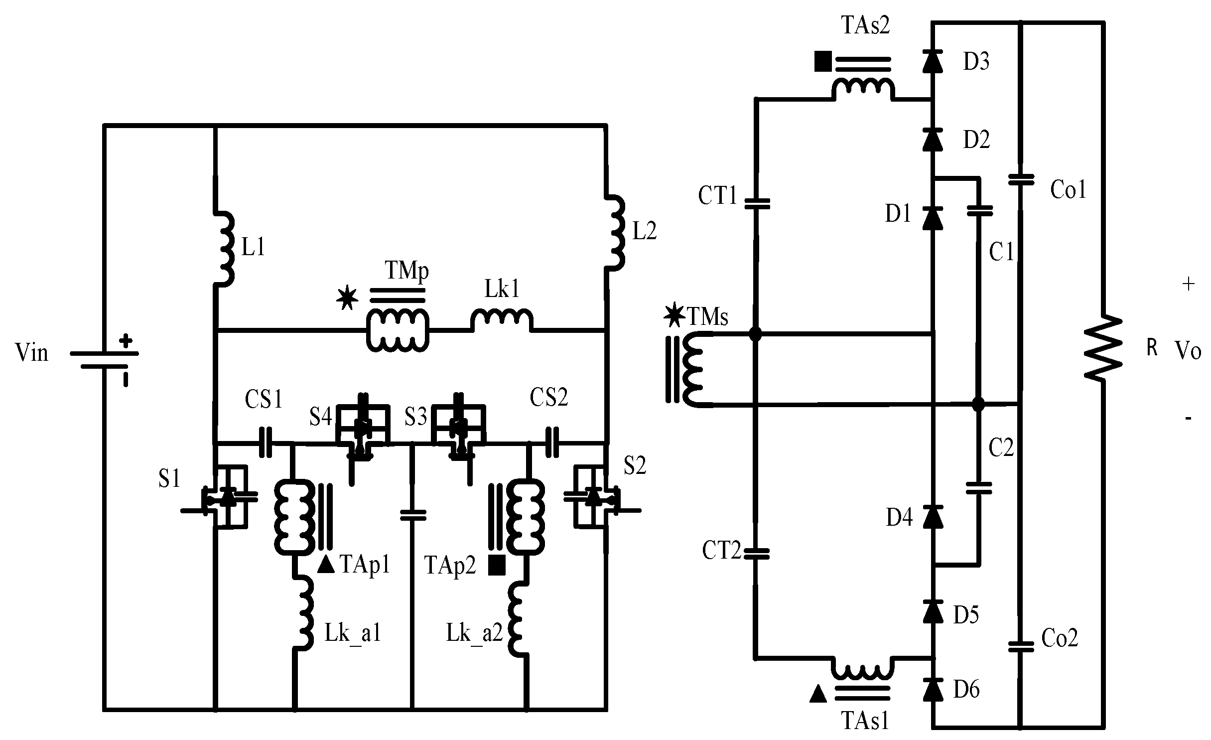
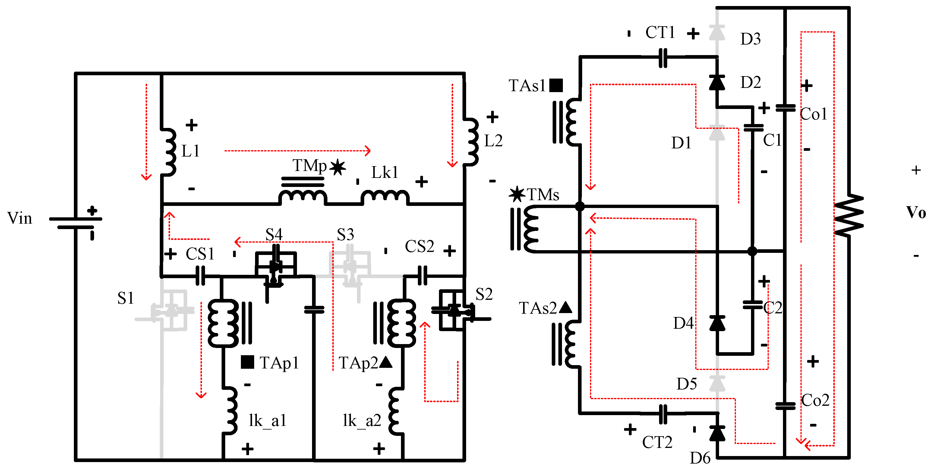
The authors of this paper propose an innovative, high voltage gain DC–DC converter using multiplier cells and 1:1 ratio transformers as seen in
Figure 2. The benefits of the 1:1 ratio main transformer can be summarized as follows:
It allows the interleaved input legs to have a series-output or half-bridge configuration.
It cuts the required duty cycle in half, since the voltage is the sum of the two cells.
The 1:1 ratio minimizes the voltage stress on diodes 1 and 4.
The auxiliary 1:1 transformer’s purpose is to construct a multiplier cell that charges capacitors CT and Co in a soft manner. The charging current will be limited by the leakage inductance of the transformer. The 1:1 ratio will help minimize the voltage stress on diodes d2, d3, d5, and d6. By adopting this configuration, a very high voltage can be produced by using very low rated components. In addition, since the two cells will share the duty cycle burden, both switching and conduction losses will be reduced with the reduction of the duty cycle. The next section details the theory of operation for the proposed converter. After that, the design equations and how this converter compares to other works in terms of voltage gain and switch voltage stress are presented. Experimental results from a 450 laboratory prototype are then presented, and an efficiency study is presented. Finally, a conclusion and considerations for future work are put forward.
2. Theory of Operation
The switching states of the converter and Kirchhoff’s voltage and current law (KVL and KCL) equations describing each switching state are described next.
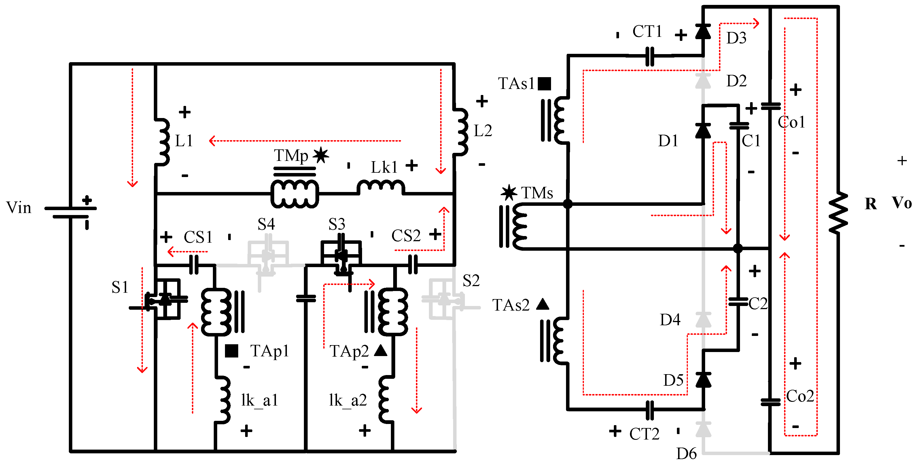
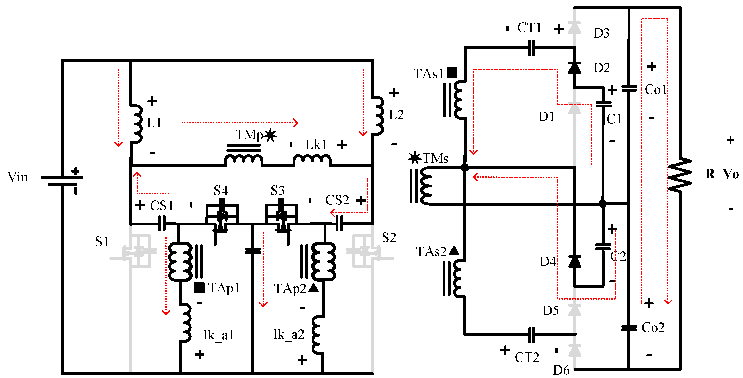
A. First state; (t0–t1) S1 -> on S3 -> on S2 -> off S4 -> off:
In this case, Diodes 1, 3, and 5 are on, and Diodes 2, 4, and 6 are off. C1 is being charged by the main transformer, and Co1 is being charged by the main transformer, CT1, and the auxiliary transformer. On the other hand Capacitor CT2 is being charged by the main transformer, the auxiliary transformer, and C2. Capacitor Co2 is discharging the load as seen in
Figure 3.
KVL equations during this state are:
where
is the turn’s ratio for the auxiliary transformers; and the KCL equations during this state are:
CS1 is now being discharged into the auxiliary transformer multiplier cell, and the clamp capacitor and CS2 are completing their charging process from the previous state. After the capacitors are charged and in the same switching state, the clamp capacitor starts feeding the auxiliary transformer and CS2 starts discharging into the main transformer.
B. Second state; (t1–t2) S1 -> off S3 -> on S2 -> off S4 -> on:
In this case, S1 turns off and the main transformer current starts circulating through S3 and S4. The current of Auxiliary Transformer 1 descends to zero and diode D3 turns off. Capacitors CS1 and clamp capacitor are charged and the capacitor CS2 continues to discharge in a decreasing manner. In other words, the capacitor continues discharging but at a slower rate as seen in
Figure 4.
The capacitor CT2 continues to be charged by C2, the main transformer, and the auxiliary transformer 2. KVL equations during this switching state are:
And the KCL during this switching state is:
C. Third switching state; (t2–t3) S1 -> off S3 -> off S2 -> on S4 -> on:
When S3 turns off, the output of the capacitor of S3 starts charging and the capacitor of S2 starts discharging. When the capacitor of S2 is fully discharged, its body diode starts conducting providing a ZVS condition for switch S2 to be turned on at the end of this switching period.
D. Fourth Switching state; (t3–t4) S1 -> off S3 -> off S2 -> on S4 -> on:
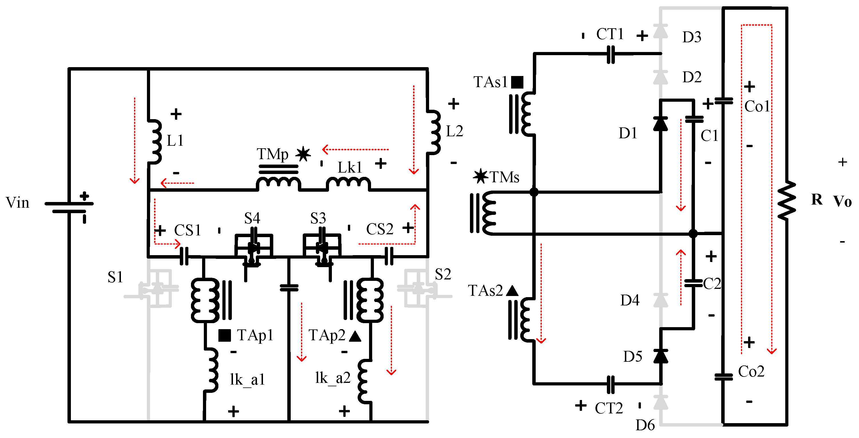
In this case (
Figure 5), Switch two is turned on. Diodes 2, 4, and 6 are on, and Diodes 1, 3, and 5 are off. C2 is being charged by the main transformer and Co2 is being charged by the main transformer, CT2, and the auxiliary transformer. On the other hand Capacitor CT1 is being charged by the main transformer, the auxiliary transformer, and C1. Capacitor Co1 is discharging on the load. KVL equations during this state are:
And KCL equations during this state are:
CS2 is now being discharged into the auxiliary transformer multiplier cell, and the clamp capacitor and CS1 are completing their charging process from the previous state. After the capacitors are charged and in the same switching state, the clamp capacitor starts feeding the auxiliary transformer and CS1 starts discharging into the main transformer.
E. Fifth Switching state; (t4–t5) S1 -> off S3 -> on S2 -> off S4 -> on:
In this case (
Figure 6), S2 turns off and the main transformer current starts circulating through S3 and S4. The current of the Auxiliary Transformer 2 descends to zero and diode D6 turns off. Capacitors CS2 and the clamp capacitor are charged, and the capacitor CS1 continues to discharge in decreasing order. Capacitor CT1 continues to be charged by C1, the main transformer, and Auxiliary Transformer 1. KVL equations during this switching state are:
And the KCL equations during this switching state is:
F. Sixth switching state; (t5–t6) S1 -> on S3 -> on S2 -> off S4 -> off
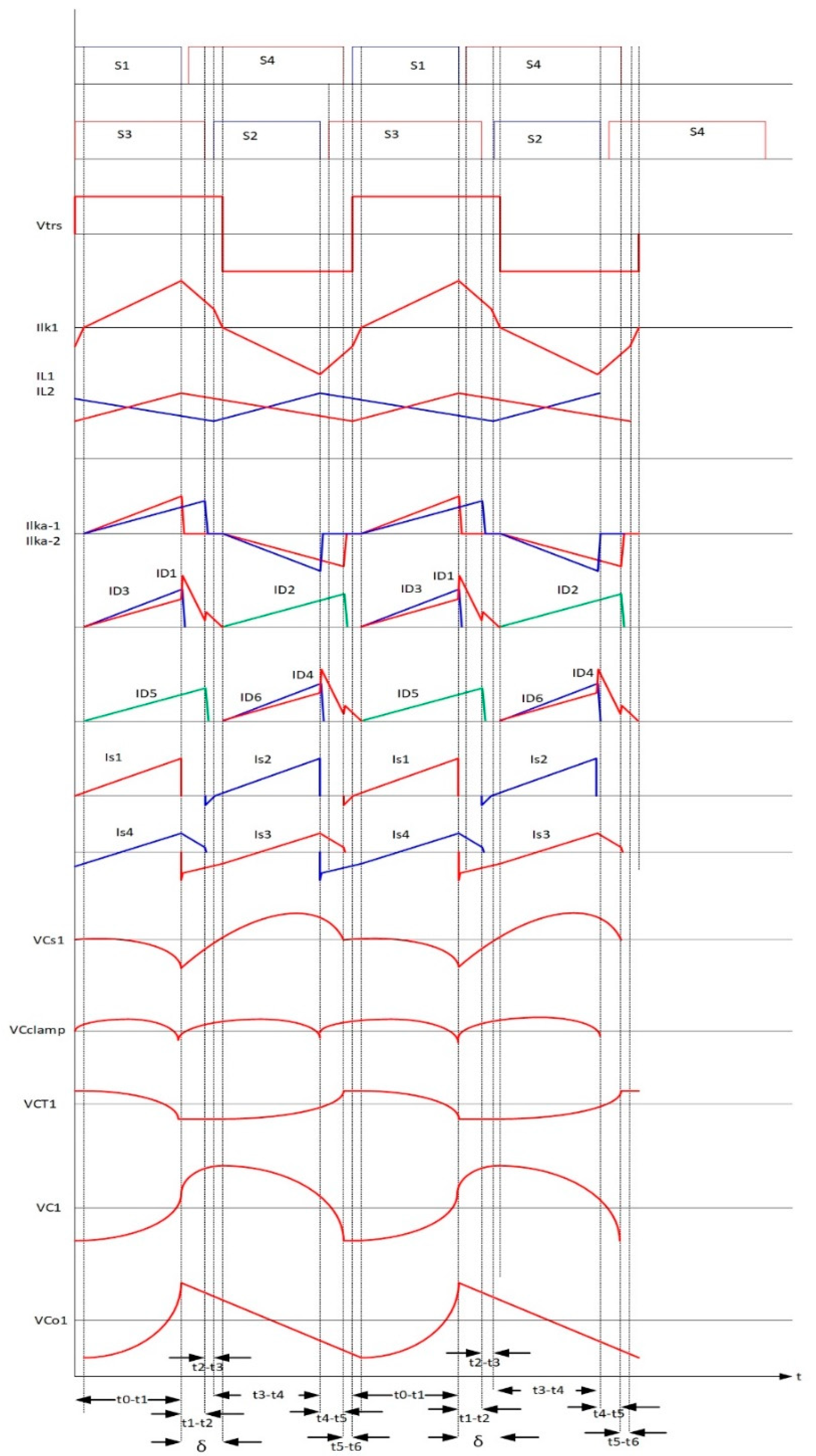
When S4 turns off, the output of the capacitor of S4 starts charging and the capacitor of S1 starts discharging. When the capacitor of S1 is fully discharged, its body diode starts conducting providing a ZVS condition for switch S1 to be turned on at the end of this switching period. The waveforms that describe the operation of this converter are presented in
Figure 7:
3. Voltage Gain and Design Equations
From the previous set of equations, the voltages of the capacitors and the currents of the inductors can be decided for the converter. In these following equations, the turns ratio of the main transformer and the auxiliary transformers is considered to be 1:1, and the leakage inductances lk-a1 and lk–a2 are considered to be very small, much smaller than the magnetizing inductances of their transformers, and therefore their voltage drops are neglected for the purposes of designing equations for the capacitors and are considered equal to each other. From the
V–sec balance on L1 and L2 we find:
Similarly, from the
V–sec balance on Lk1 we find:
where
δ is the period where the leakage current of the main transformer reaches zero. Since the voltage drop on the leakage of auxiliary transformers is negligible:
And the output capacitors voltage is equal to:
And the output voltage of the Converter is calculated as:
From the conservation of energy principle:
Since each input inductor shares half the current, the average current on each inductor is:
And from the average current on D1:
Solving this integration with respect to
δ would lead to a long series of terms to be arranged and would finally lead to an equation defining
δ as:
From which
δ can be found and
Q is defined as:
After finding
δ, the peak current of the leakage current can be found to be what follows:
And the capacitor values based on the desired ripple percentage should be:
For the design of the transformer, the area product method was used. To select a core size for the transformer, the following equation was used:
where
the maximum desired flux density in the core and J is the desired current density in the wires. From the Area product that is calculated here a proper core can be chosen if it has a higher area product that is calculated from the datasheet. After that, the number of turns can be calculated by:
The same approach was used for the auxiliary transformers where the area product for the core selection is:
And the number of turns can be found as:
For the leakage inductor design, a gapped core with well-known effective permeability is chosen. Then the number of turns is calculated as:
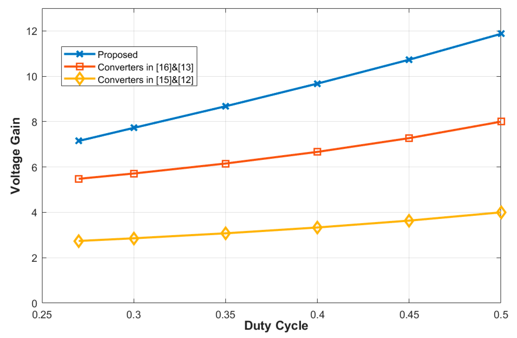
The next figure (
Figure 8) shows the voltage gain compared to other referenced works and it shows that the voltage gain is much higher. It should also be noted that the considered voltage gain for the proposed converter is the practical voltage gain that takes into consideration the drop effect off the leakage inductance, while other converters’ voltage gains are the ideal ones.
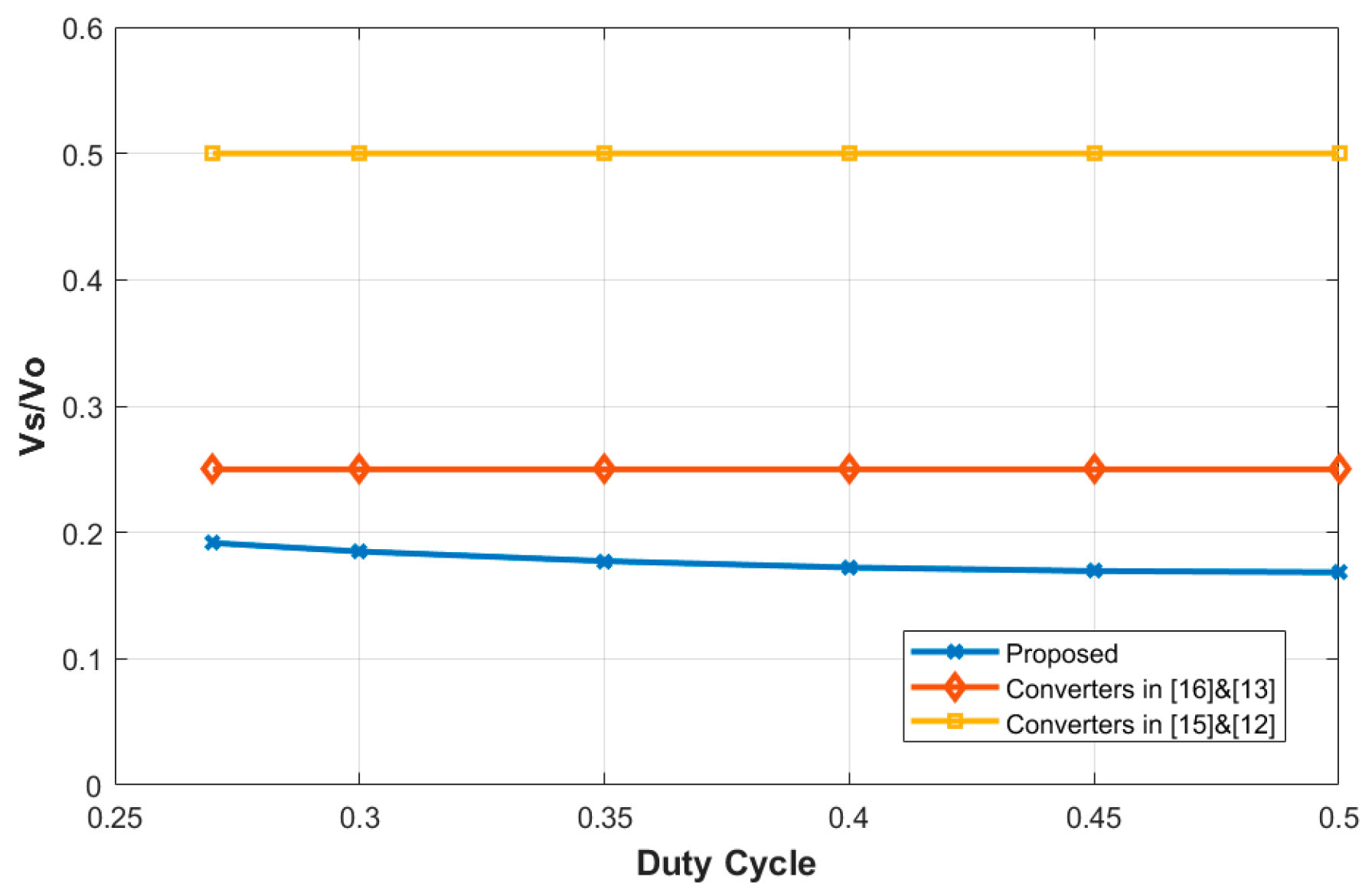
The normalized switch to voltage ratio for the proposed converter compared to others is in
Figure 9.
It can be seen that the normalized switch voltage ratio is much smaller than compared topologies, which allow for the utilization of lower-rated switches.
4. Experimental Results
A 450 W prototype was developed in the laboratory to validate the concept of this converter, and the parameters and components in
Table 1 and
Table 2, respectively, were used.
The first experiment was performed as a proof of concept to validate the analysis made in chapter two.
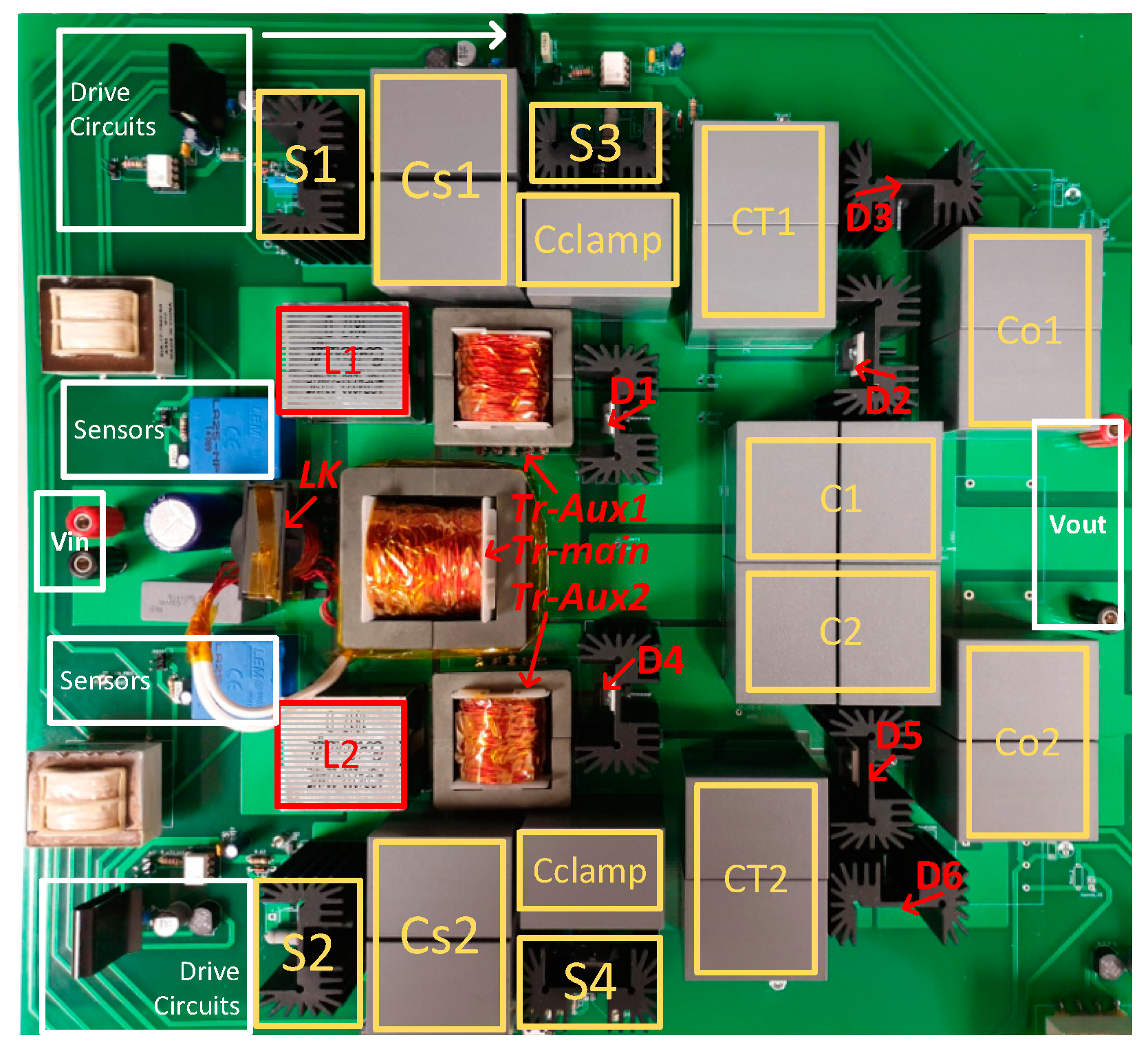
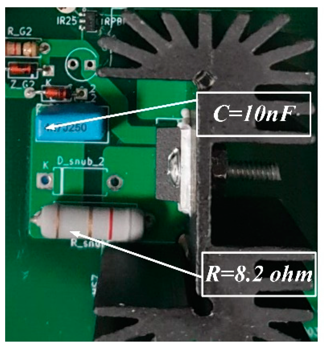
Figure 10 shows the designed prototype and its layout. The current of the input inductors is measured through 2 LA 25NP sensors. The switches are being driven by FOD 3182 drivers with isolated floating supplies. In addition, each switch is equipped by an RC snubber to prevent over voltages from parasitic inductances at turn offs. The RC snubber consists of an 8.2 ohm resistor and a 10 nF capacitor and its layout is shown in
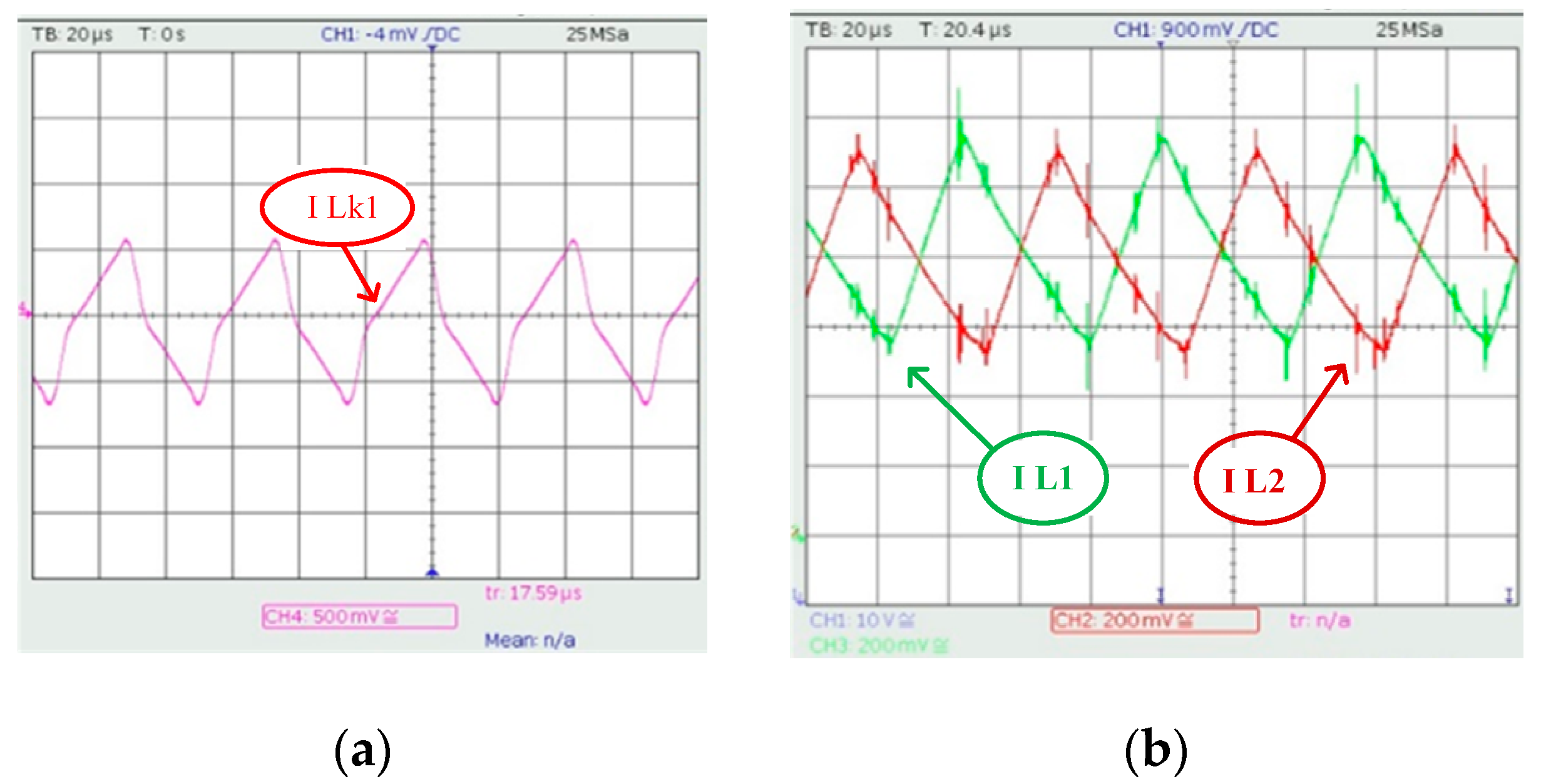
Figure 11. The converter is operated first at 320 W and output voltage of 380 volts. The input voltage is 37 volts and the duty cycle 0.4.
Figure 12a shows the current waveform of the main transformer Ilk1 which is probed by a current probe that conforms to the analysis presented in chapter two.
Figure 12b shows the two input inductors share the current equally and will effectively reduce the ripple of the input source. With the addition of capacitors at the input, combined with the interleaved structure, the source can achieve zero ripple.
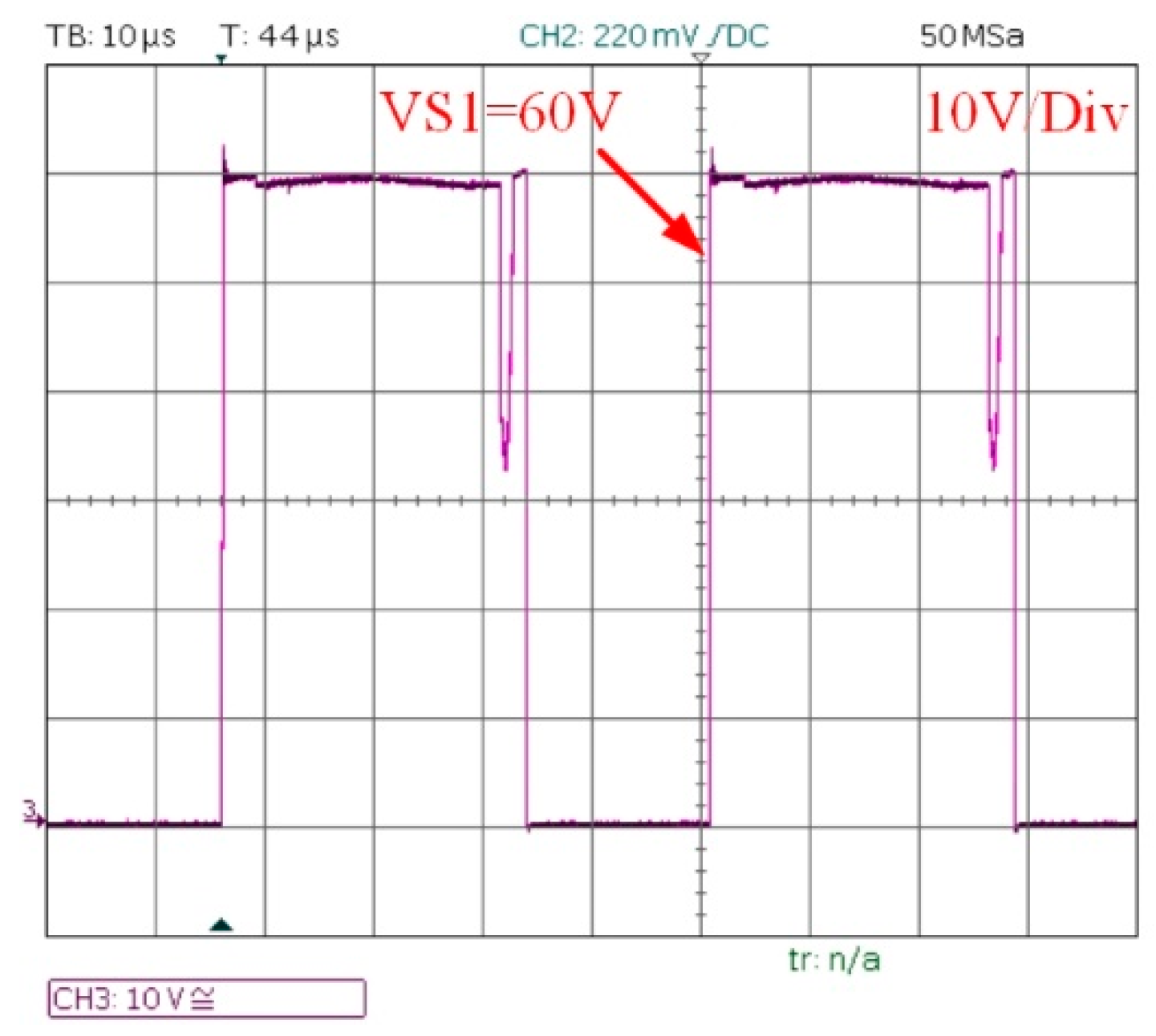
Figure 13 shows the active switch voltage when the output voltage is 380 volts, the duty cycle is 0.4, and the load is 320 W. It can be seen that the voltage stress on the switch is 60 volts which is much less than the one in [
12,
15] which would be 120 volts for the same output voltage level.
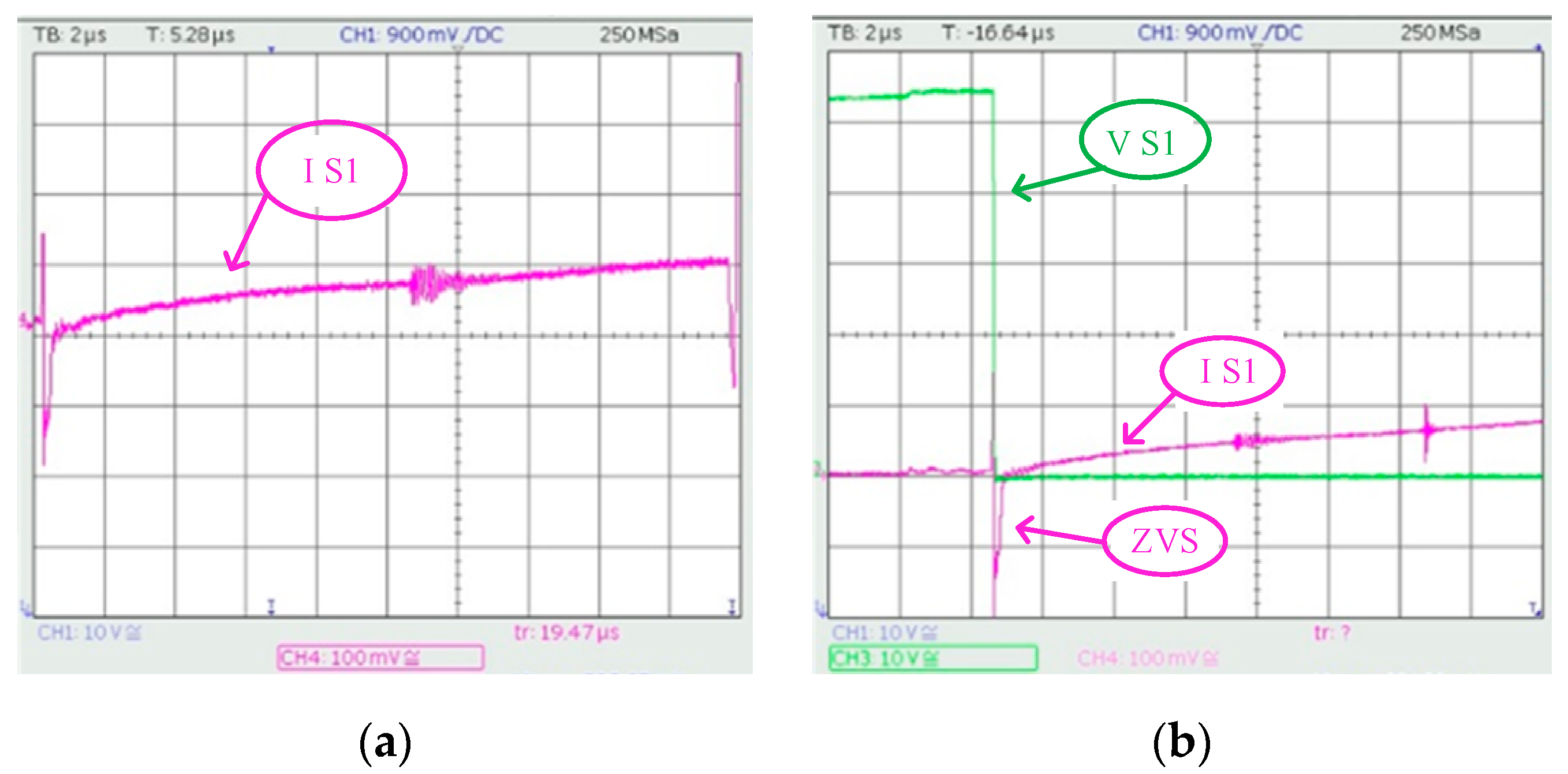
Figure 14 shows the switch currents under ZVS operation for the main and complementary switch under full load of 450 W. The other two switches have the same waveforms, only phase shifted 180 degrees.
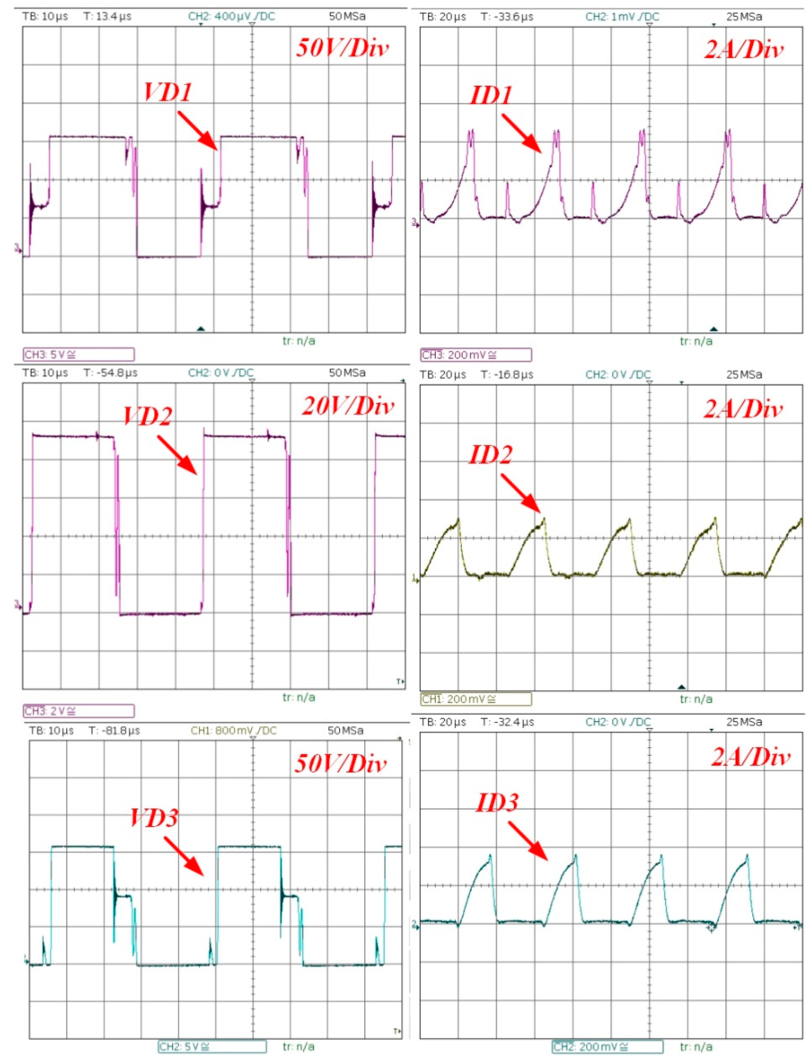
Figure 15 shows the voltages and currents of all diodes in a single leg. The other diodes have the exact waveforms, only phase shifted 180 degrees.
It can be seen that the waveforms conform to the analysis and it can be seen how Diode 1 collects all the leakages. These measurements were performed under a load of 450 Ohms and an output voltage of 380 volts.
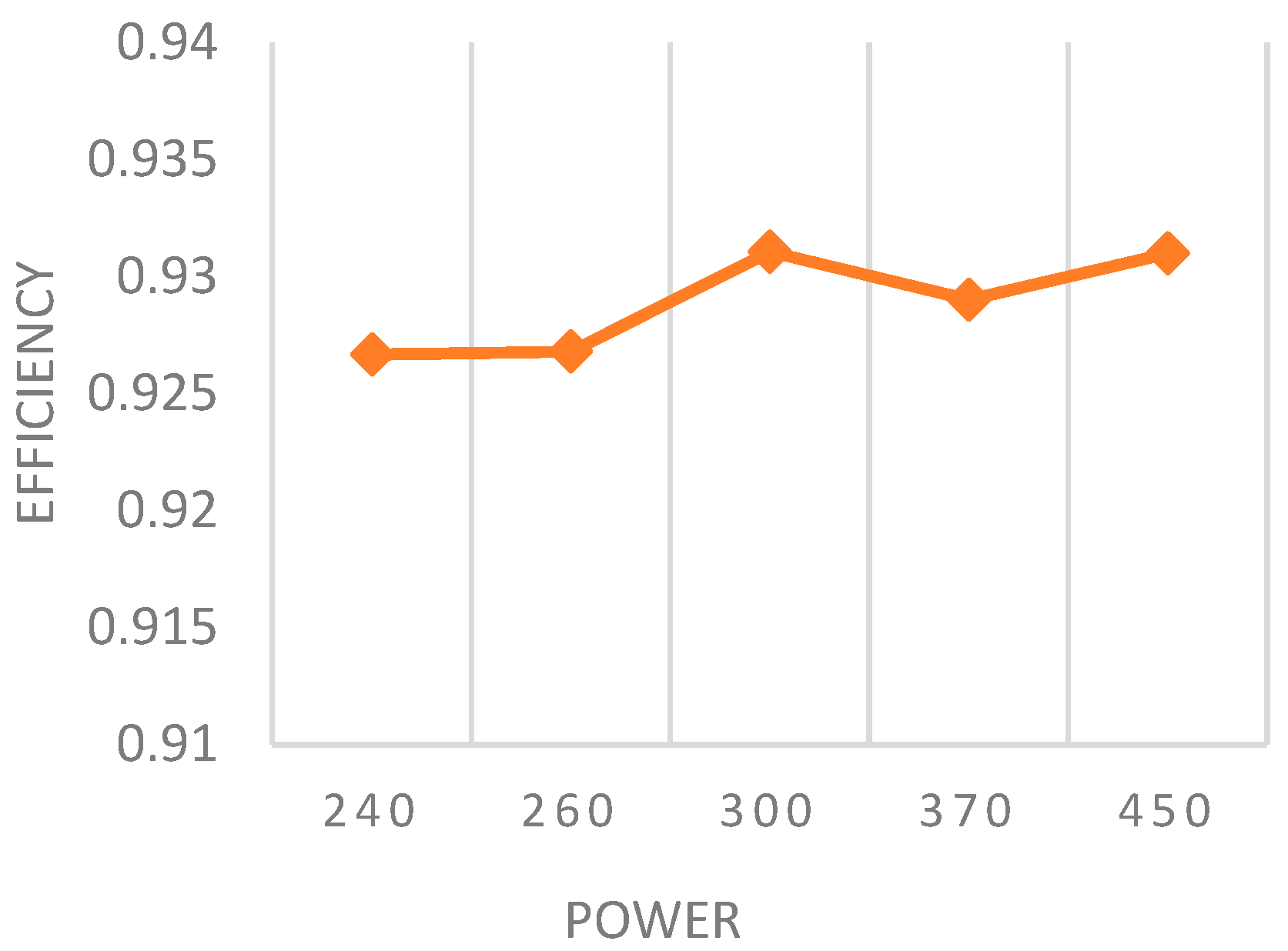
The efficiency of the converter was found by measuring the input power and the output power at different loads.
Figure 16 shows the overall efficiency of the converter during these loading conditions.
It can be seen that the converter maintains an efficiency of around 93% even at half load. The prototype from [
14], for example, drops in efficiency from 93 to 90% at half load. In addition, prototype from [
15] has a peak efficiency of 96% that drops to 89% at half load.
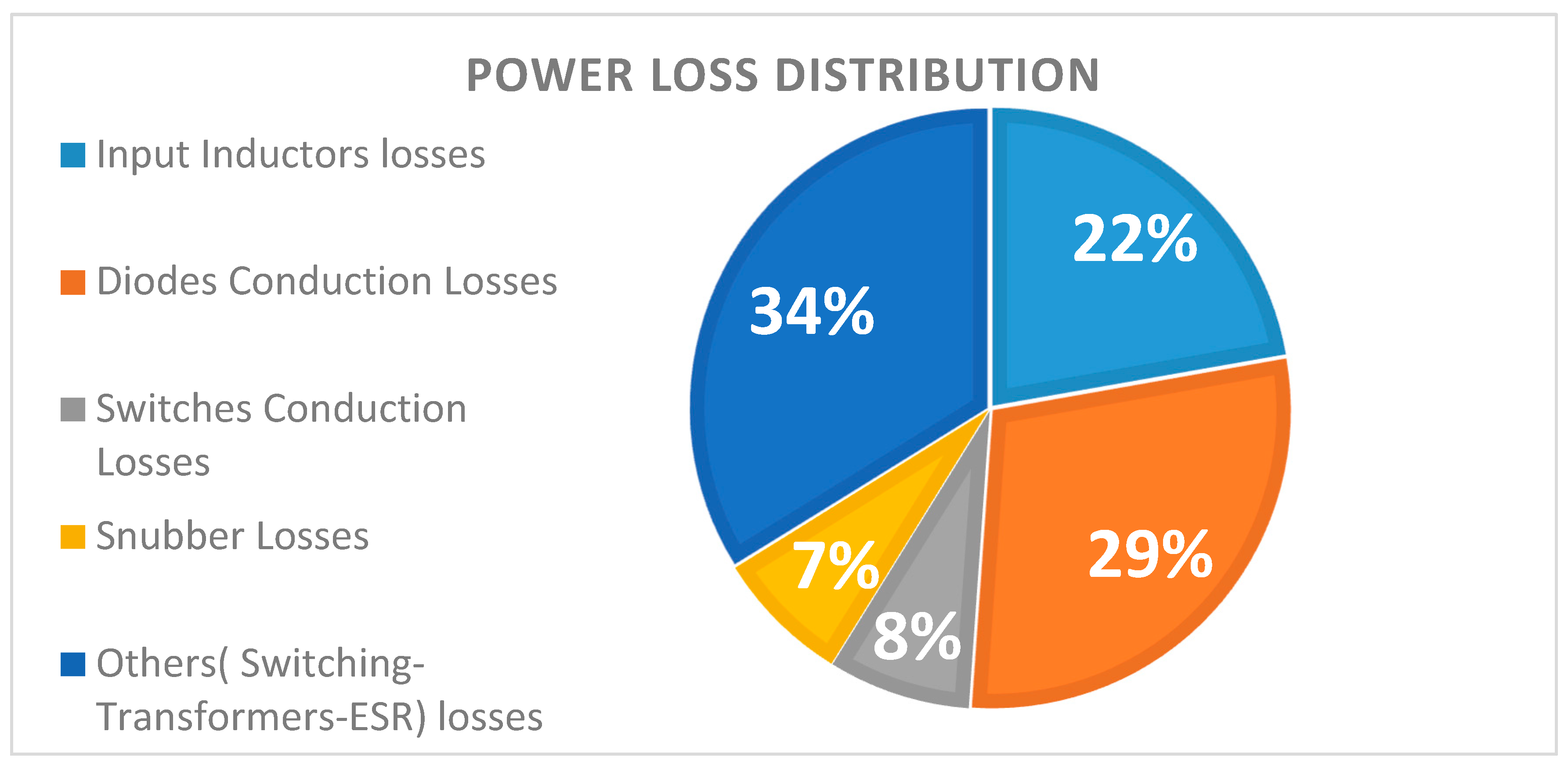
After that, a power loss distribution study was performed under a 320 W load and an output voltage of 380 volts. The losses for different parts of the converter were calculated based on measured currents and datasheet parameters. The following power loss calculations were performed:
where VFD is the diode forward voltage that is given in the data sheet and RDS on is the on resistance of the switch found in the datasheet. RL1 and RL2 are the parasitic input inductor resistances. The power loss distribution is presented in
Figure 17 and shows how losses are distributed in the converter. The transformers were built manually in the lab with a twisted pair of magnetic wires to reduce the skin effect and proximity effect. However, even though DC resistance can be measured, the effective resistance of the wires cannot be defined exactly under that switching frequency, and therefore the whole loss of the transformers was combined in the other section. The values of parasitic parameters were considered for the actual temperature and current during the calculation of losses.


