Abstract
This paper presents and discusses the careful modeling of a Zero Biased Diode, including low-frequency noise sources, providing a global model compatible with both wire bonding and flip-chip attachment techniques. The model is intended to cover from DC up to W-band behavior, and is based on DC, capacitance versus voltage, as well as scattering and power sweep harmonics measurements. Intensive use of 3D EM (ElectroMagnetic) simulation tools, such as HFSSTM, was done to support Zero Biased Diode parasitics modeling and microstrip board modeling. Measurements are compared with simulations and discussed. The models will provide useful support for detector designs in the W-band.
1. Introduction
Schottky diodes play an important role in several functions, such as rectification [1,2], mixing [3,4], and detection in all the range of microwave frequencies, up to the W-band and beyond [4].
In general, modeling of the diodes is a critical task in the design process of circuits operating at high frequencies [3,4]. Antimony (Sb) heterostructure backward diodes offer better noise performance with easier matching to 50 Ohm [5] compared to GaAs Schottky diodes, but may not always be easily accessible or available as discrete components [6]. Series 9161 diodes (Keysight HSCH and MACOM-Metelics MZBD) models are frequently used for hybrid detectors below the W-band [7,8,9], though also in the W-band [10,11,12,13]. Zero-bias Schottky diodes from ACST (Advanced Compound Semiconductor Technologies GmbH) (https://acst.de/) operating as power sensors have been reported in [14]. Zero Bias Diodes Schottky diodes from Virginia Diode Inc. (VDI) were used for W-band detection in [6,15]. Available manufacturer information (https://www.vadiodes.com/images/pdfs/Spec_Sheet_for_VDI_W_Band_ZBD.pdf) is limited and, in the absence of diode models developed by the designers themselves, commercially available models could be required.
Usually, the device modeling is accomplished by discriminating between the modeling of the intrinsic component (characterized by quasi-static I-V and C-V measurements) and the extrinsic elements (characterized by 3D Electro-Magnetic (EM) tools, along with the measurement of the Scattering parameters at some specific bias points). In [16], modeling techniques are presented to extract a Schottky diode model analytically using additional fabricated structures (such as short and open circuits) for the de-embedding of parasitic capacitances and other effects. Unfortunately, it is not always possible to have such customized cal kit (calibration kit) structures available. Previous efforts in Schottky diode modeling of Single Anode (SA) VDI devices were presented in [17]. In this paper, ZBD (Zero Bias Diode) devices from VDI have been carefully modeled, considering two different diode-mounting techniques to attach them to the final circuit assembly: wire bonding and flip-chip (also known as controlled collapse chip connection). From DC measurements, the intrinsic nonlinear current source, along with the parasitic resistor can be obtained. Scattering measurements of the ZBD provide data which can be used to identify the parasitic and extrinsic elements up to the W-band; in this sense, in Section 2, the modeling of ZBDs for wire bonding assembling is presented. In Section 3, the modified model oriented to the flip-chip attachment technique, obtained from the previously extracted diode model, is shown; low-frequency noise sources are included in the complete diode model in Section 4. Finally, some conclusions are drawn in Section 5.
2. Nonlinear Zero Bias Diode Modelling
Modeling of the ZBD was based on the procedures presented in [16,17]. Firstly, a 3D model of the passive parts for EM simulation (HFSSTM) was built based on microphotographs (Figure 1) and physical measurements of the critical dimensions, performed with a Scanning Electron Microscope (SEM) available in the Laboratory of Science and Engineering of Materials of the University of Cantabria (LADICIM).
Figure 1.
(a) General View of the ZBD using SEM (Dice about 600 × 250 µm; anode finger length about 100 µm). (b) Detail of the anode finger of the ZBD (diameter about 9 µm). Reference scale is at the bottom of the figures.
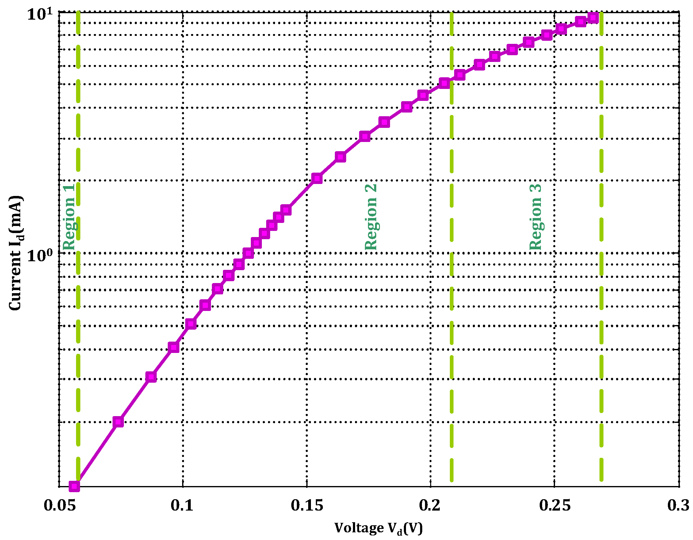
2.1. DC Measurements and Nonlinear Model
For modeling purposes, as a starting point, the diode equivalent circuit presented in Figure 2 is here considered. In this circuit, the main non-linearities (Id Current Source and Cj Capacitance), as well as parasitic elements due to metallization (Rs) and packaging (Cpp, Cp, and Lf), can be observed.
Figure 2.
Diode equivalent circuit model.
Using a specific high-accuracy voltage-controlled current source to ensure both protection of the device during the test process and accurate current/voltage measurements in the low current level region (below 1 mA), the static I/V characteristic of the ZBD was measured (Figure 3). By means of proprietary extraction software, the value of the thermionic-field emission model parameters [18] for the nonlinear current source (1) were obtained (Table 1).
Figure 3.
I-V measured current for the ZBD Schottky diode under testing.
Table 1.
Extracted value of parameters in Equation (1).
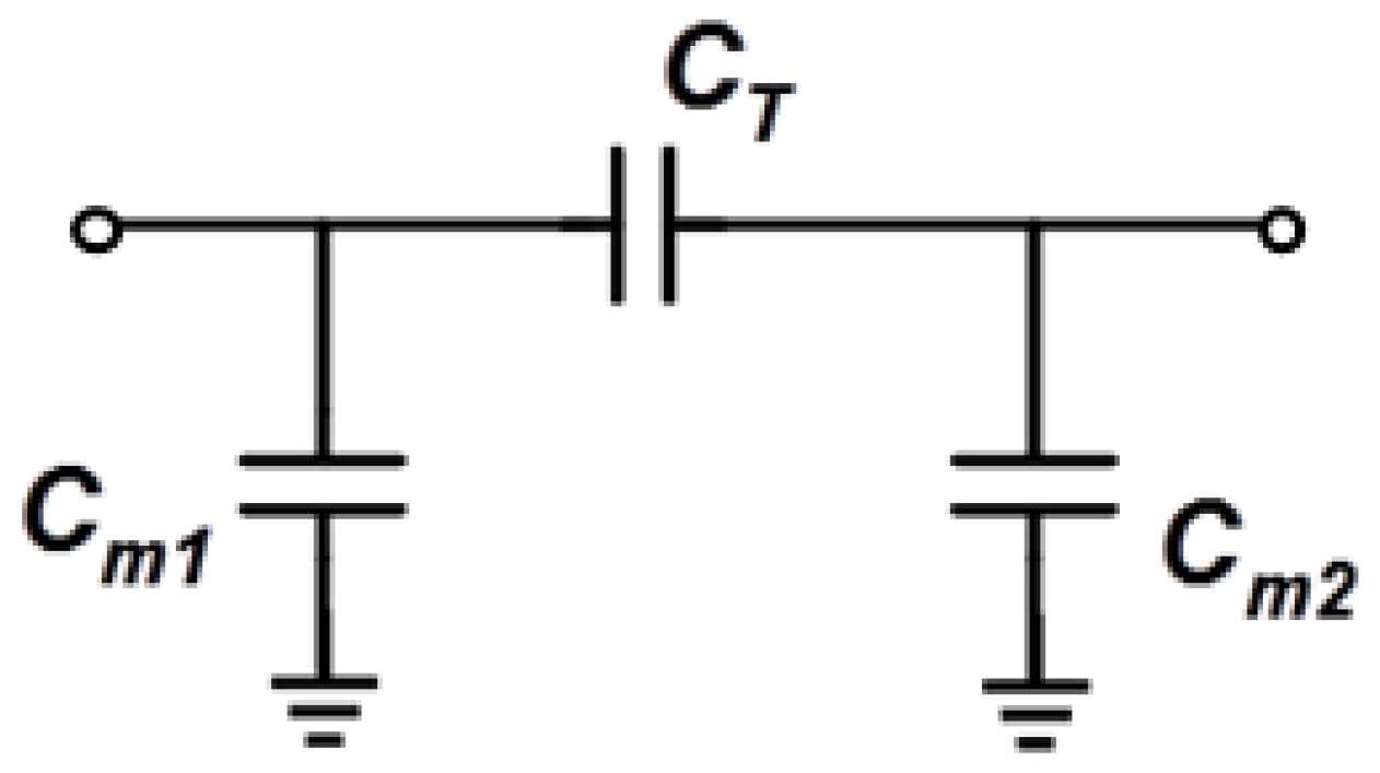
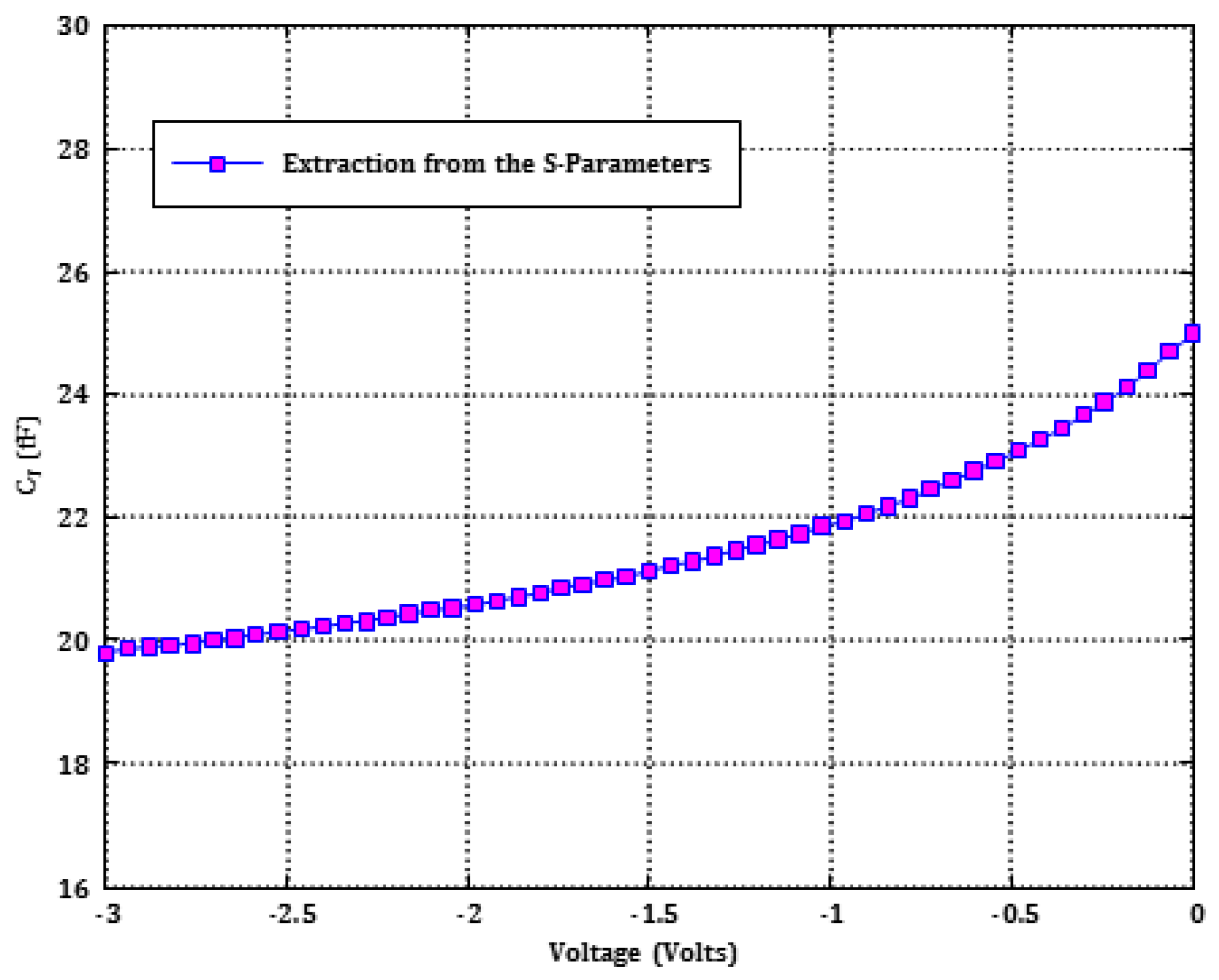
2.2. Low-Frequency Model
At lower microwave frequencies, the equivalent circuit of the unbiased, or negatively biased, diode can be reduced to a “π” electrical network of capacitances, as depicted in Figure 4.
Figure 4.
Low-frequency equivalent circuit model of the passive diode.
The above “π” network accounts for the total capacitance CT, as well as the small-value parasitic capacitances to the ground (if considered), Cm1 and Cm2, where CT is the sum of the junction capacitance Cj and the parasitic capacitances Cpp, as shown in Equation (2).
An accurate estimation of the total capacitance can be extracted from the measured value of the S21 scattering parameter (Figure 5) when a negative bias, Vd, is applied to the diode. Parameter S21 essentially depends on the total capacitance, CT (the junction capacitance Cj at Vd = 0 V, Cj0, junction potential, , and the parasitic capacitance Cpp). Scattering parameters of the diode were measured from 2 GHz up to 50 GHz; however, for capacitance extraction purposes, only the frequency range of 3–10 GHz was used, considering the equivalent circuit in Figure 4. By varying the negative Vd voltage applied to the diode, and performing the measurement of the scattering parameters of the diode at each voltage, it was possible to extract the values of the CT capacitance as a function of this voltage. In Figure 6, the extracted Capacitance versus Voltage (C-V) plot is presented. In Table 2, the values of the elements of the circuit in Figure 2, as well as the parameters of Equation (2), are presented.
Figure 5.
Measurements and modelling of transmission coefficient for the unbiased (Vd = 0 V) ZBD.
Figure 6.
Results for the extraction of total capacitance of the ZBD from scattering parameters.
Table 2.
Value of parameters of Equation (2).
In principle, the results obtained in the extraction from the S-parameters offer more accurate estimations of nonlinear and parasitic capacitances of this diode, compared to other extraction methods based on low-frequency impedance measurements. This also avoids other potential problems of low-frequency measurements, such as uncertainty in the de-embedding of the parasitic effects of probes.
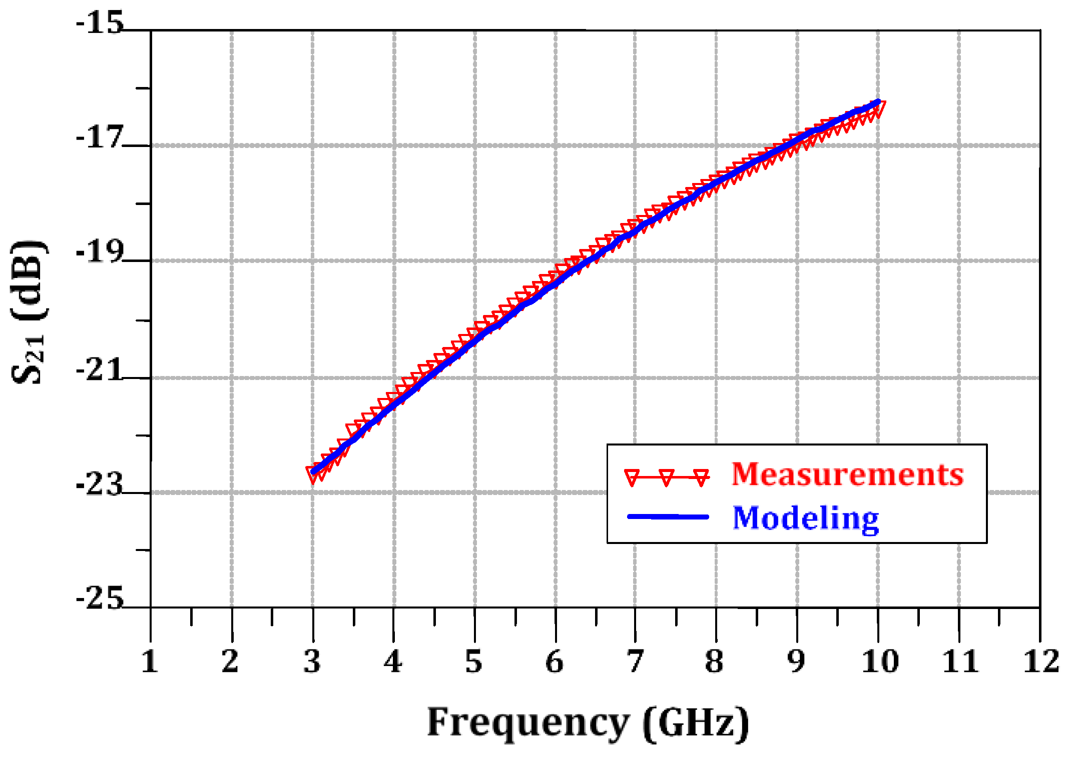
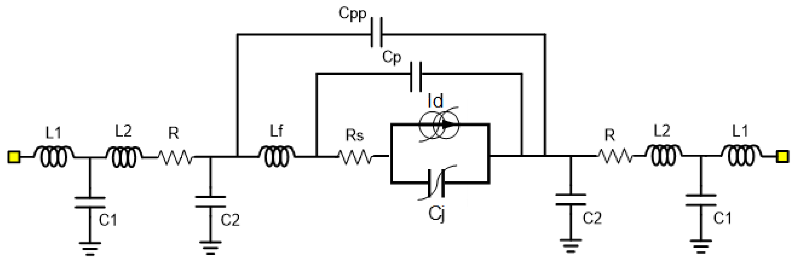
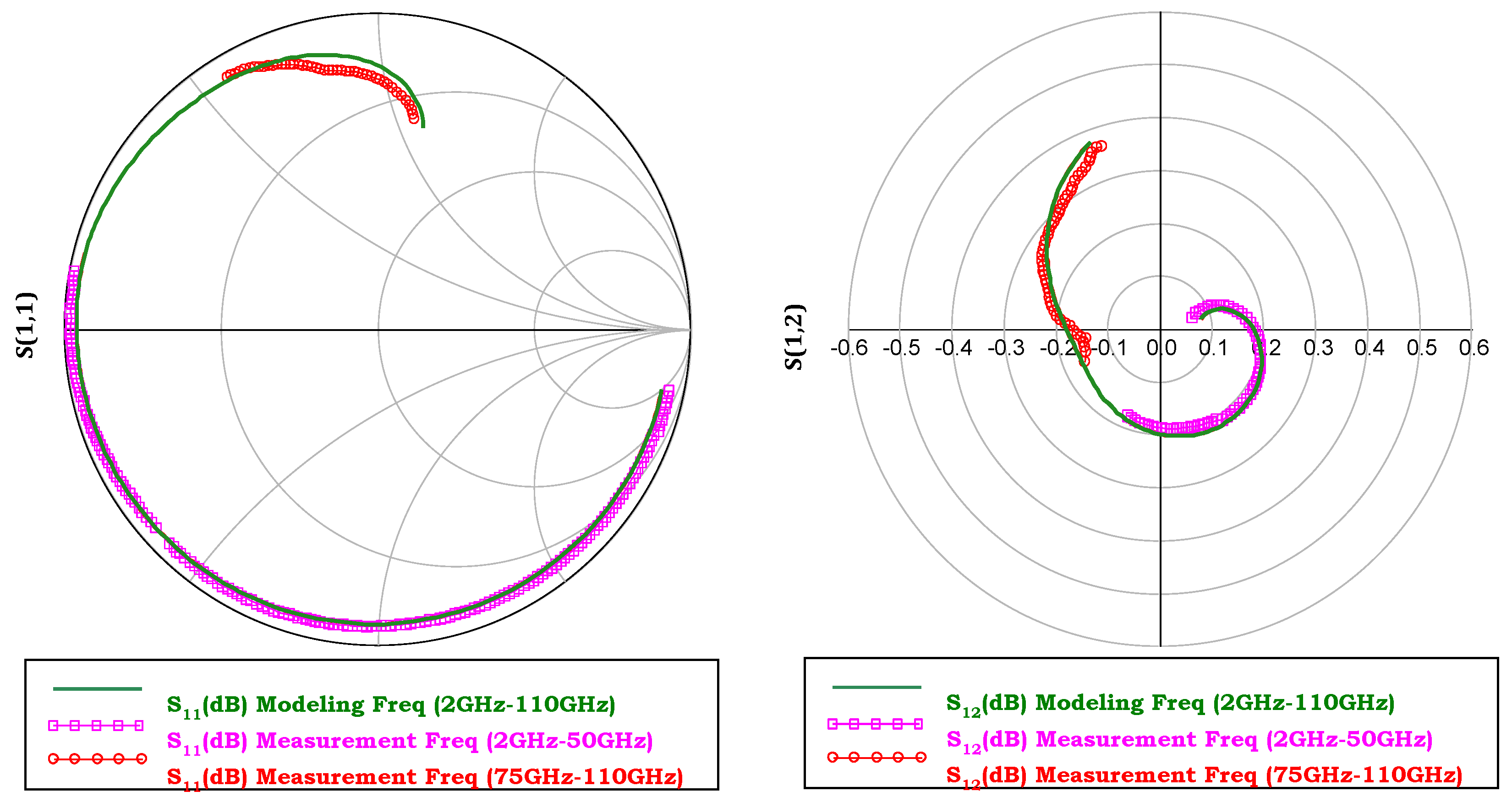
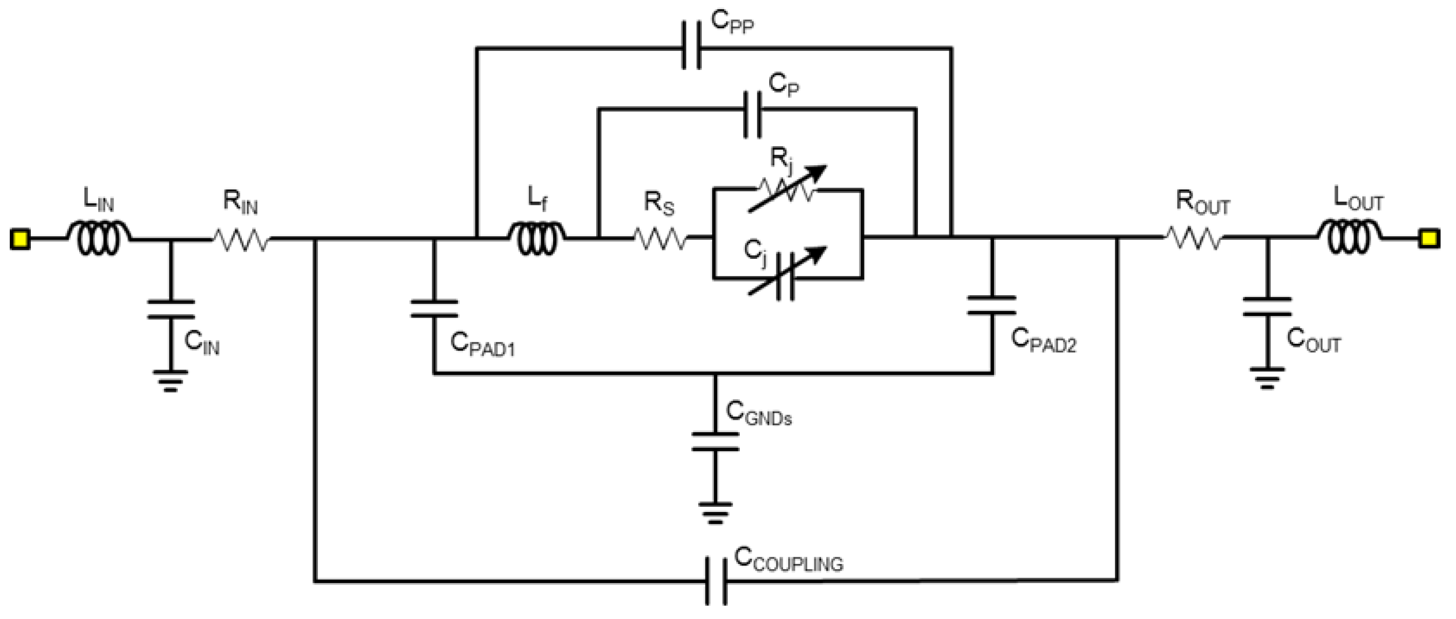
2.3. Modified ZBD Model Up to W-Band
At high frequencies, from 75 GHz up to 110 GHz, additional parasitic effects arise which affect the behavior of the diode; thus, it is critical to evaluate and model them. This is really a complex task due to the difficulties involved in the de-embedding process of the access elements, such as coplanar-to-microstrip (CPW-M) transitions and bonding wires used in the circuit assembly to implement the input and output connections. This is the reason why, although the diode is usually considered as a one-port element, with the cathode or the anode grounded, we are going to perform measurements being anode and cathode the electric ports, considering the diode as a two-port electrical network, allowing to identify the effect of grounding.
Firstly, modeling of the coplanar to microstrip (CPW-M) transitions was performed, as reported in [17]. Once the model of the CPW-M transition was obtained, the modeling of the ZBD, when using the wire bonding attachment technique, was possible from the measurements performed at the coplanar probe station using a LRRM (Line-Reflect-Reflect-Match) calibration. A de-embedding procedure in Keysight ADS™ [19] was performed considering the previously obtained model of the CPW-M transition along with the gold bonding wire model.
In Figure 7, the reflection and transmission coefficients from the equivalent circuit simulation are compared with the experimental measurements in two frequency ranges (2–50 GHz and 75–110 GHz) for the unbiased diode (Vd = 0 V). From these results, it can be concluded that the degree of agreement between both results is excellent. Therefore, the modeling procedure proposed provides a model that can simulate the behavior of ZBD from the DC up to 110 GHz.

Figure 7.
Modelled and measured [S]-parameters of the unbiased diode (0 V) after the de-embedding in the wire bonding configuration.
An increase in the series resistance value was observed in the W-band measurements; this singular behavior can be associated with the skin effect above 50 GHz, the bonding wires, and probably some other measurement uncertainties. The study of the extent of this effect becomes difficult in this frequency band as measurements are limited by calibration accuracy, as well as some possible inaccuracies in the determination of other equivalent circuit parameters, such as finger inductance and parasitic capacitances. Nevertheless, the increase in resistance in the W-band was consistently found when fitting measurements of several devices, as previously reported in the literature [20].
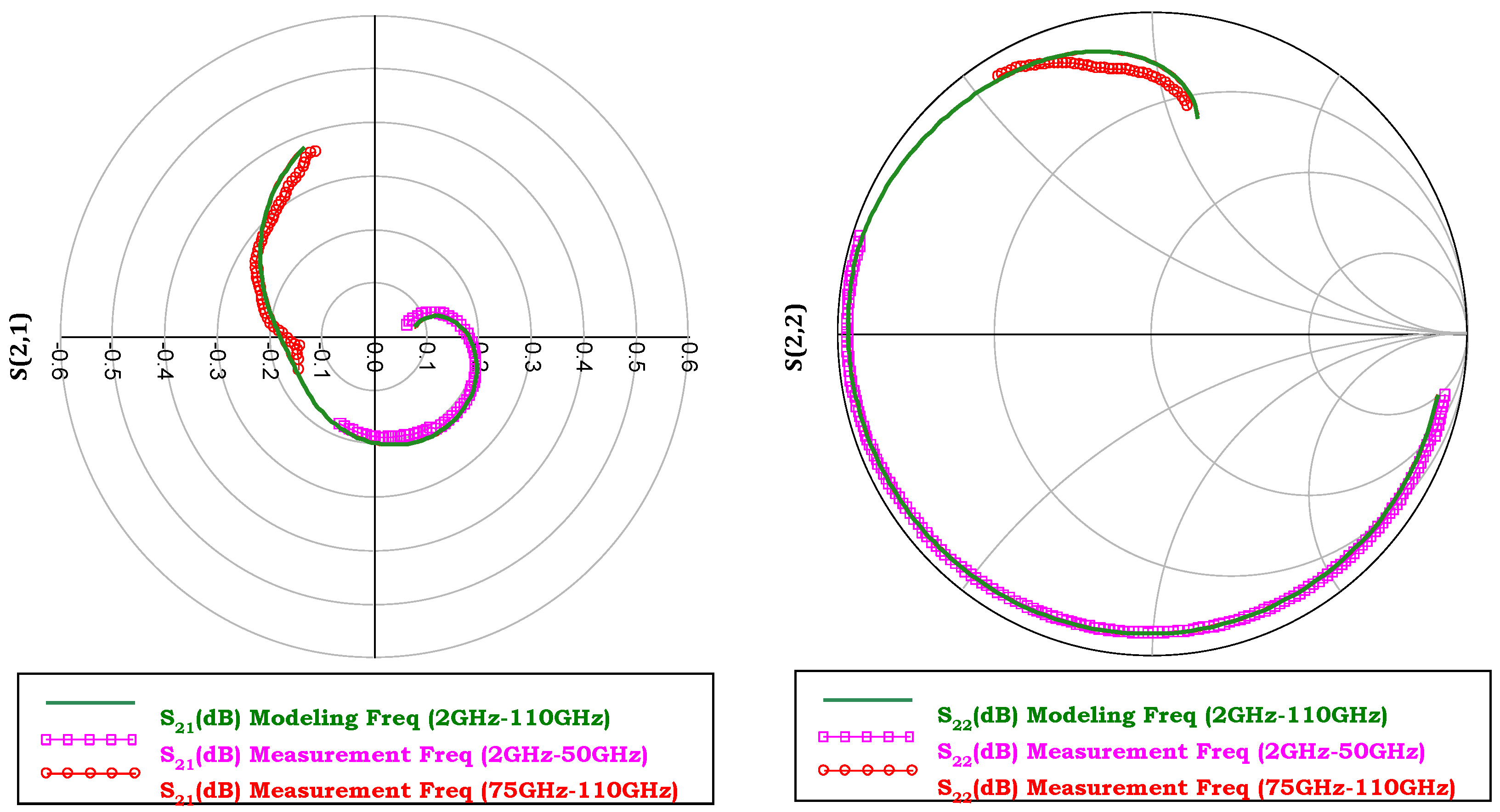
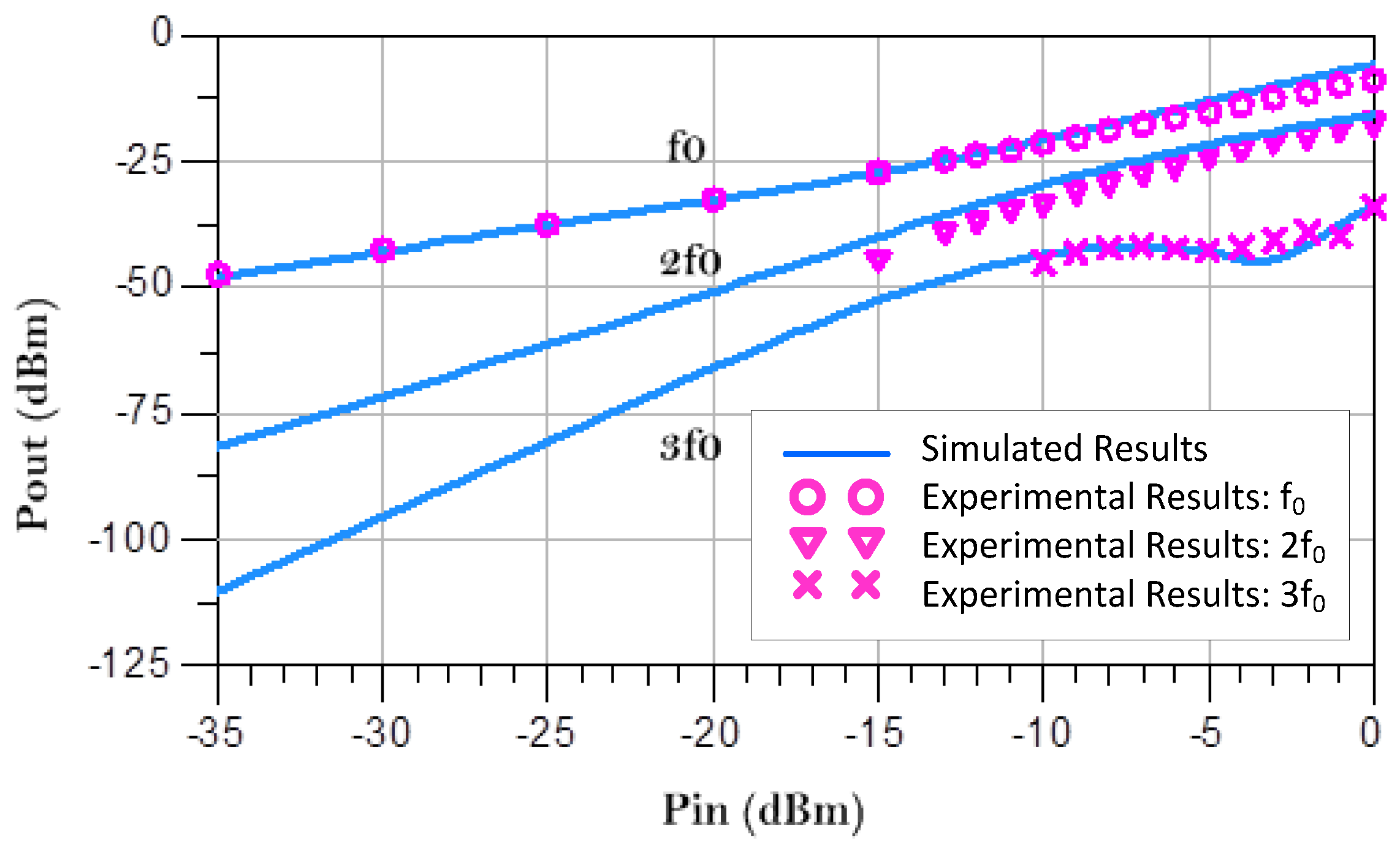
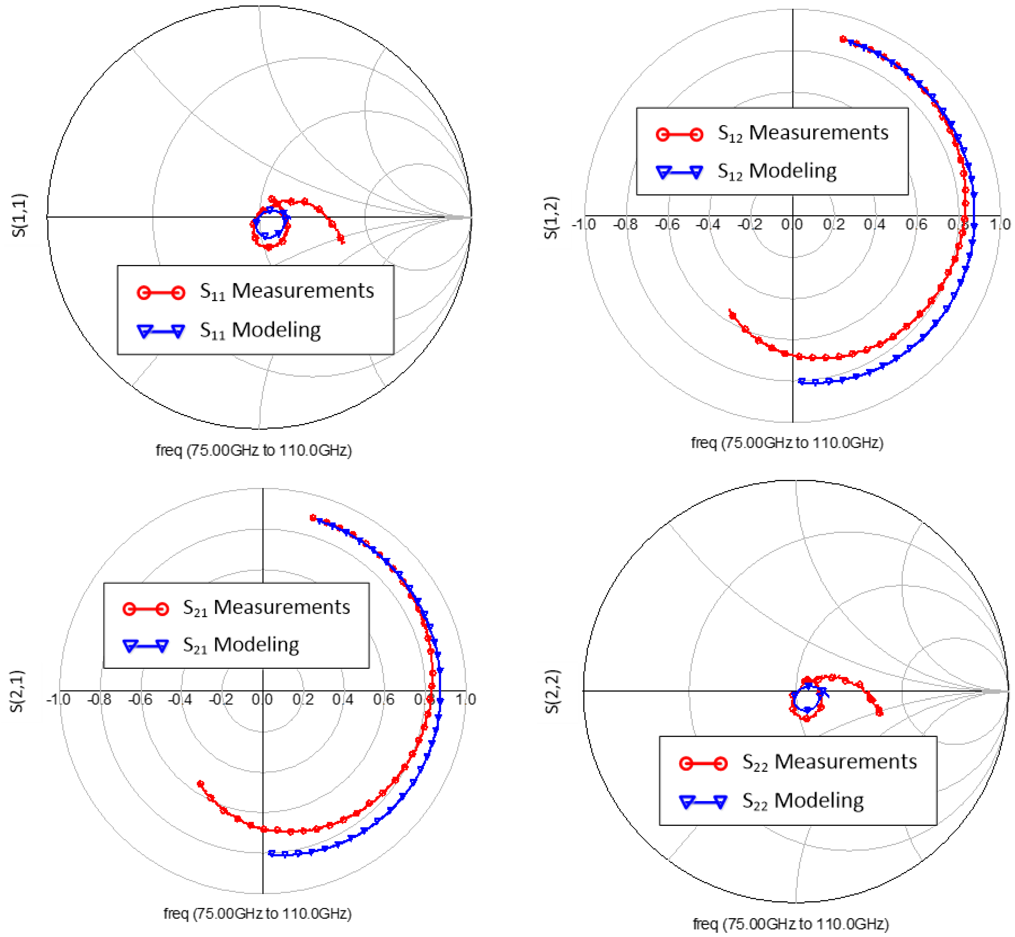
2.4. Large Signal Model Extraction and Validation
The final topology of the proposed diode’s large signal model is shown in Figure 8 [6].
Figure 8.
Equivalent circuit model of the diode, including the extrinsic elements.
In Table 3, the values of the model parameters obtained from the different measurements performed using the extraction procedures [16,17] are presented. In this model, Cp represents the finger-to-pad capacitance between the anode contact finger and the underlying active GaAs. The bonding resistance, R is fixed to 0 Ohm at “low frequencies”, while its value equals to 3 Ohm in the W-band.
Table 3.
Extracted values of the parameters for the ZBD model.
In order to validate the large-signal model of the diode, output power versus input power measurements were compared with harmonic balance simulations performed in Keysight ADS™ [19]. In Figure 9, comparisons between measurements and simulations, when a signal of 1 GHz is applied to the device, are depicted. In this graph, a reasonable global agreement between measurements and simulation results can be seen at the fundamental frequency and the second and third order harmonics. If we focus on the highest input power level, simulations tend to overestimate the first harmonic, while the second is more accurate as the power is higher. The third harmonic is well-estimated in values, but with slight differences in the slope. This could be due to several reasons: the source current mode was originally intended to simulate the nonlinear current source in DC conditions; however, the large-signal behavior depends on the model’s ability to predict harmonics, something that, in general, is difficult to guarantee as it requires a more elaborate development of the nonlinear current source model. Furthermore, the influence of nonlinear capacitance should be considered, which could require a more accurate characterization at the highest power levels.
Figure 9.
Simulated (continuous line) and measured output power versus input power. (Circles: f0, Inverted Triangle: 2f0, Cross: 3f0).
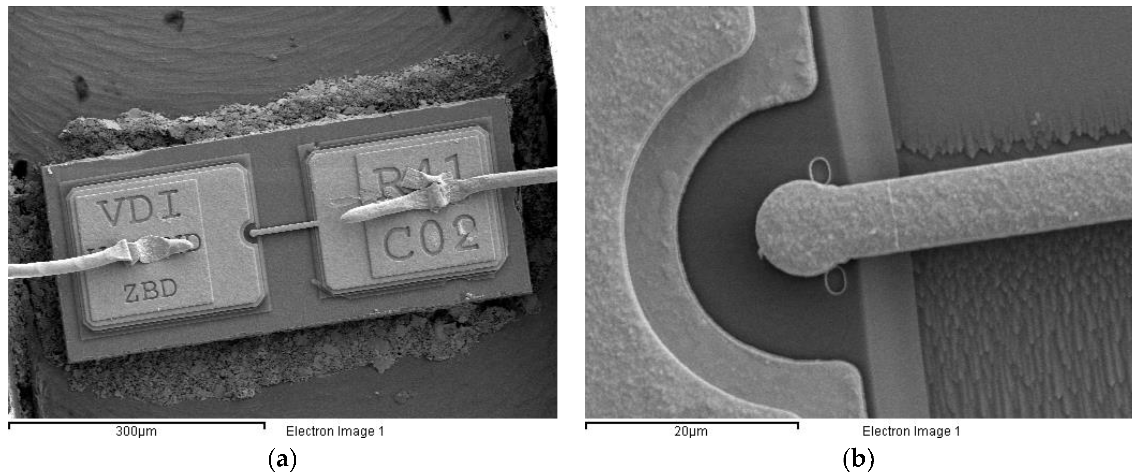
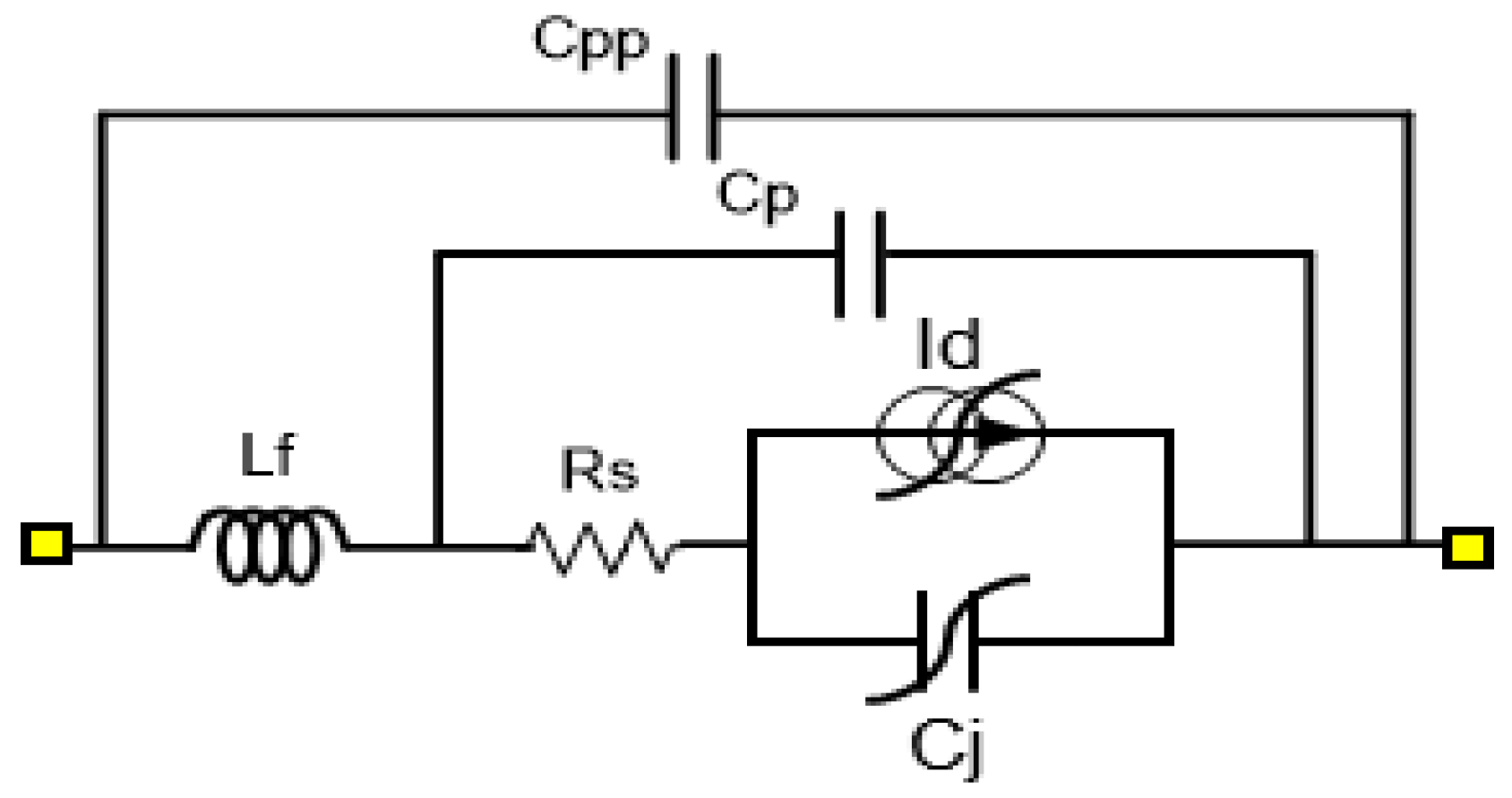
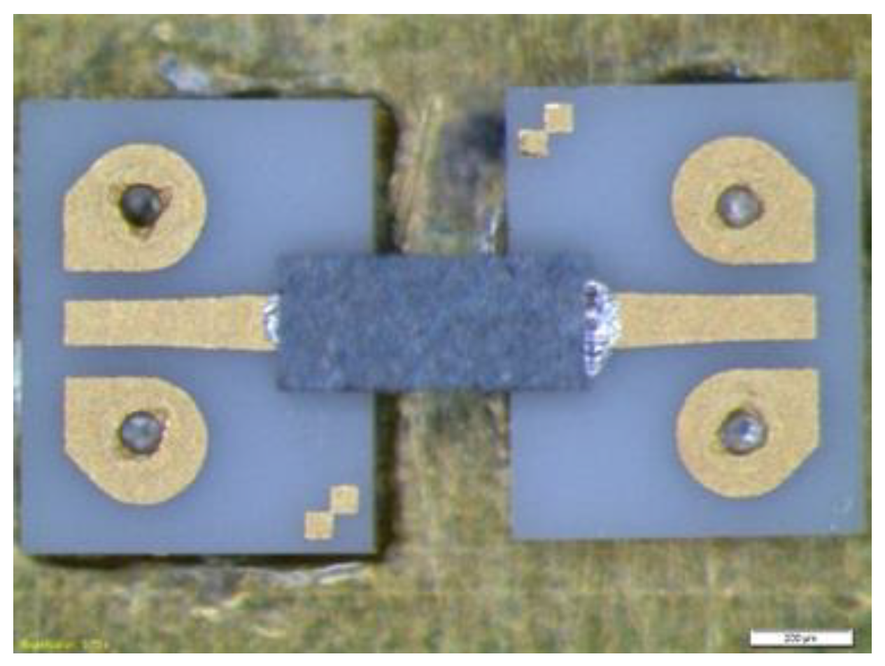
3. Diode Modelling Oriented to Flip-Chip Attachment Technique
The previous model is a basic general-purpose model, but particularly considering W-band applications, it was necessary to achieve a better approximation for the most commonly used attachment technique of the ZBD to the circuit assembly, while being well-based on the previously presented model extraction. Therefore, a new circuit was assembled by attaching a ZBD using the flip-chip technique, as shown in Figure 10. This attachment technique is the most critical in terms of the location of the diode, in order to achieve a symmetrical structure and to avoid destroying the finger of the diode by placing it in contact with the CPW-M transition. Please note that, to attach the flip-chip into a circuit, the chip must be inverted to bring the solder dots (made of H20E silver epoxy) down onto the connectors on the circuit board; then, the solder is re-melted (120 °C for 15 min) to produce an electrical connection, leaving a small space between the diode and the underlying mounting.
Figure 10.
Photo of the ZBD in the flip-chip assembly.
As performed for the previously presented modeling procedure, CPW-M transitions were used, and their model was used in the optimization in Keysight ADSTM, in order to obtain an equivalent circuit model consisting only of the intrinsic and parasitic elements of the diode. A comparison between experimental measurements and the model (described below) simulation results is shown in Figure 11, showing a better match at the lower frequencies of the W-band.
Figure 11.
Comparison between S-parameter measurements and modeling simulation of the unbiased ZBD (0 V) for the flip-chip assembly in the W-band.
Flip-Chip Zero Bias Diode Complete Model
The resulting equivalent circuit model is presented in Figure 12. Comparing this equivalent circuit with the previous model (Figure 8), the main difference is that some capacitances have been added to account for some newly existing parasitic effects. In the flip-chip assembly, the diode was attached to the carrier upside down, compared to the conventional mode with bonding wires. Therefore, capacitances C2 in Figure 8 are identified in Figure 12 as CPAD1 and CPAD2, being connected to a new capacitance, CGNDs, which represents a new, slightly capacitive coupling effect between the microstrip reference plane of the diode bulk and the ground plane of the total circuit assembly. An additional capacitive coupling effect is thus originated, CCOUPLING, which is related to the capacitive coupling between the CPW-M transitions since, in this assembly, both transitions are placed closer than in the previous one. The LIN-CIN-RIN and ROUT-COUT-LOUT electrical networks simulate the microstrip line effect at the connection between the diode and the CPW-M transition; besides, RIN and ROUT also include the losses related to the H20E conductive silver epoxy used to attach the diode. It should be emphasized that fitting in Figure 7 covers the range from 2 to 110 GHz, de-embedding the effect of the wire bonding, while Figure 11 covers a frequency range from 75 to 110 GHz, comparing measurements and simulations without de-embedding. The upside-down positioning of the diode causes some uncertainty in the parasitic capacitances with the ground, but at the same time, other parasitic elements must be maintained for coherence with grounded-microstrip ZBD model (Figure 8). Those restrictions limit the capability for a perfect impedance matching.
Figure 12.
Equivalent circuit model for the ZBD in flip-chip assembly.
The resulting model parameters extracted for this second diode assembly technique are listed in Table 4.
Table 4.
Results of the parameter extraction of the total capacitance of ZBD.
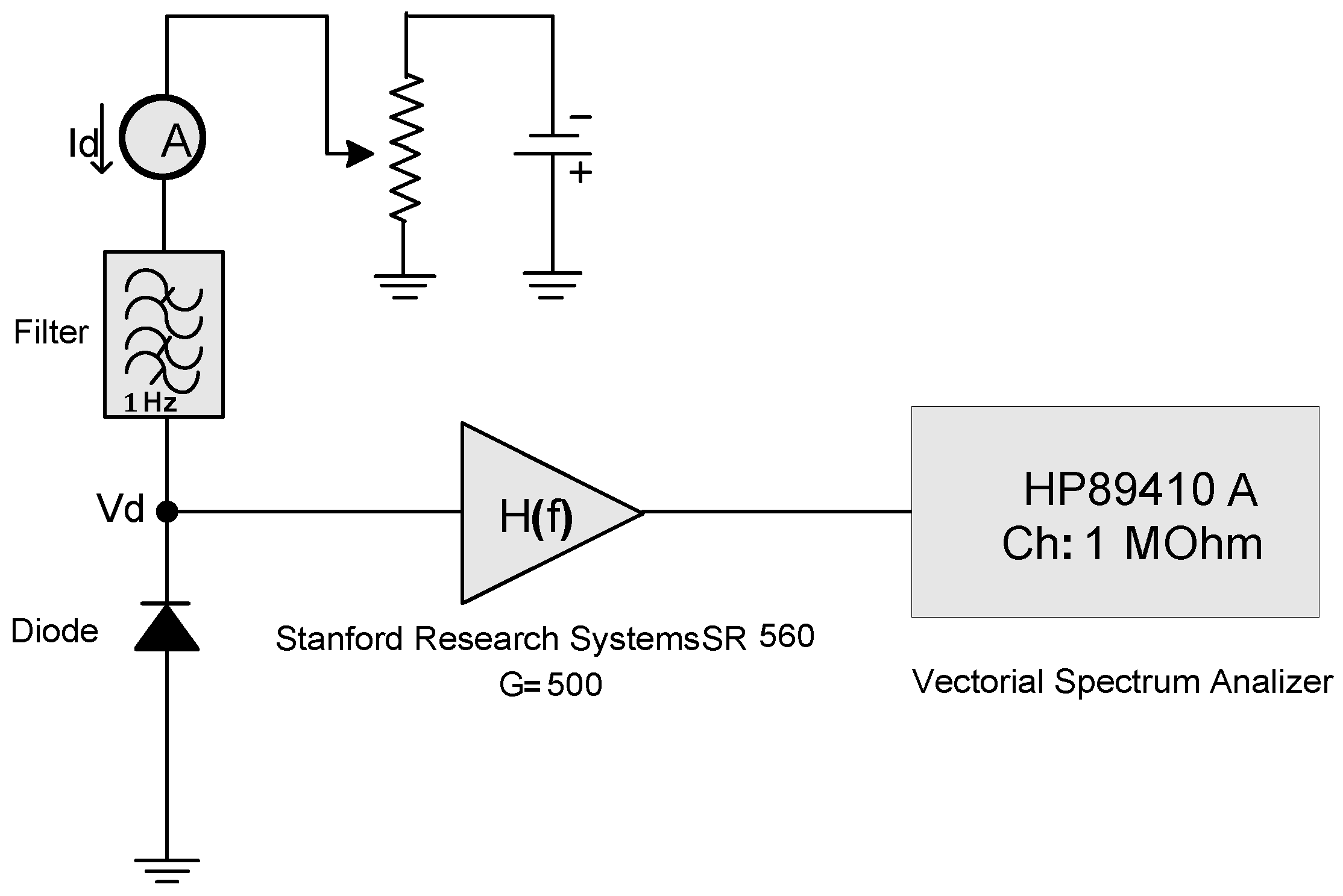
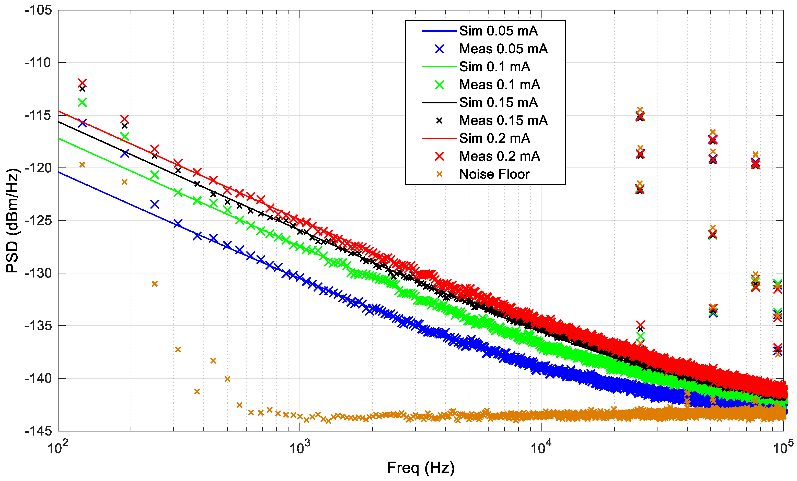
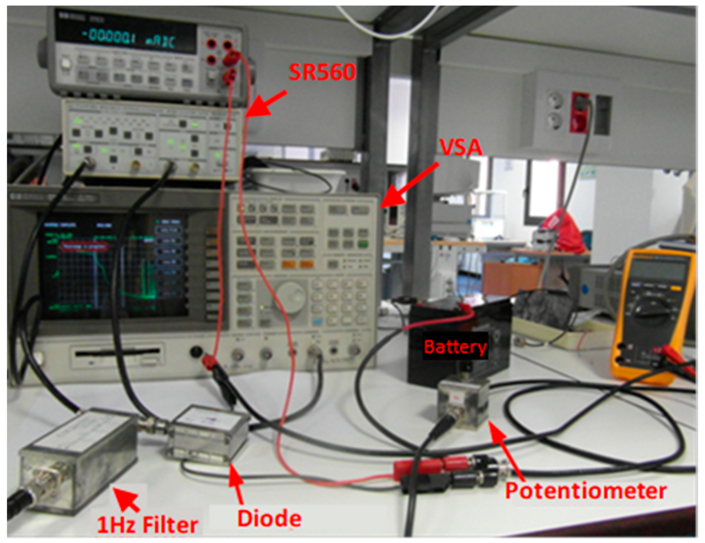
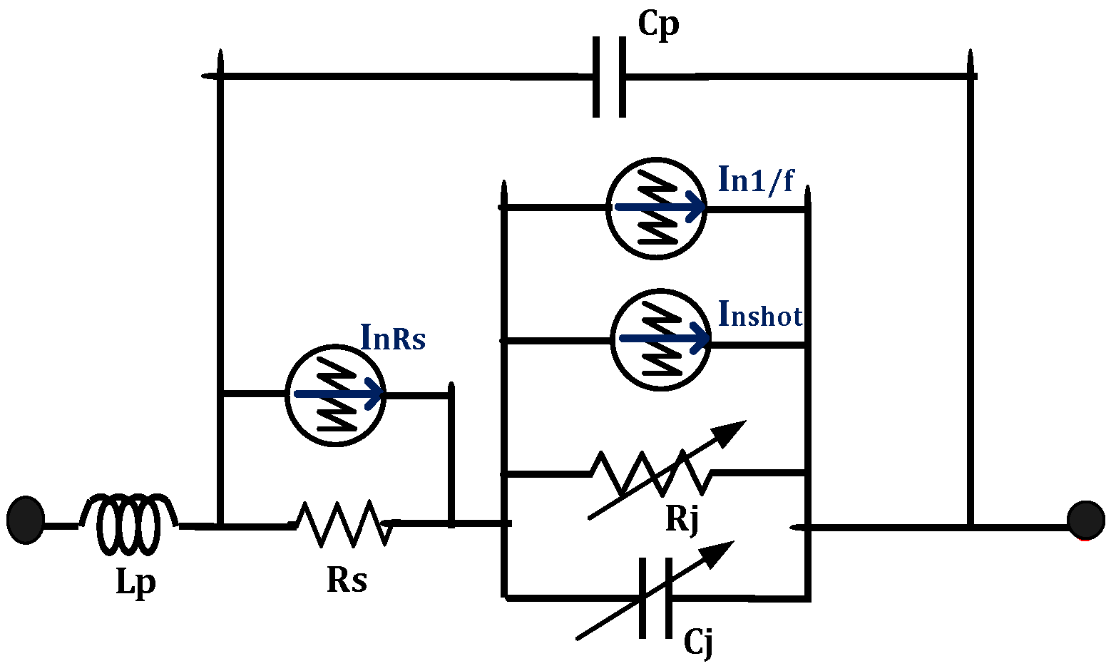
4. Including Low-Frequency Noise in the Zero-Bias Model
For a complete evaluation of diode performance, which is of significant use in detectors, a knowledge of low-frequency noise behavior becomes quite relevant—not only as proof of technology quality, but also to establish the noise floor, which limits the dynamic range. Thus, this ensures a stable response in a dynamic mode of operation. In this sense, a set-up was developed to measure and model low-frequency noise sources present in the ZBD, following [9]. The set-up diagram is shown in Figure 13, and the corresponding photo is shown in Figure 14. In this case, the diode was mounted in the conventional way (grounded, not Flip-Chip) inside a shielded box to avoid unwanted interference in the measurements. In this low-frequency range, a distinction between the flip-chip and wire bonding is not relevant.
Figure 13.
Setup to evaluate low-frequency noise under different DC biases.
Figure 14.
Photo of the measurement setup for low-frequency noise, corresponding to the diagram in Figure 13.
The main low-frequency noise contributions expected in the current spectral density (CSD) were: thermal noise associated with the series resistance Rs, shot noise, and flicker noise. The equations governing the different noise sources are given in Equations (3)–(5) (where K is the Boltzmann constant, f is the low frequency, q is electron charge, Is is the saturation current, and Idiode is the actual current, whereas Kf, af, and bf are parameters to be determined). Noise sources were placed in the circuital model of the diode, as shown in Figure 15.
Figure 15.
Insertion of noise sources in the diode model.
The low-frequency noise spectrum measured with the set-up in Figure 13 and Figure 14 is shown in Figure 16, including the system noise floor (NF trace) and measurements for the four different current bias points: 0.05 mA, 0.1 mA, 0.15 mA, and 0.2 mA. The set-up was also simulated considering all the noise contributions and Flicker noise parameters in Equation (5), which were optimized to fit with the measurements at these four bias currents. In Table 5, the optimized parameters are listed.
Table 5.
Low-frequency noise parameters.
5. Conclusions
In this paper, two models for Zero-Biased Diodes (VDI) considering wire-bonded or flip-chip techniques have been presented, with particular emphasis on the flip-chip model in the W-band. Equivalent circuit models were complemented with the extraction of low-frequency noise sources (Flicker) and its incorporation in the proposed models, allowing for a more complete prediction of the response of the diodes, for example, in detectors. The obtained models were validated under different operating conditions, and power prediction abilities of the model were probed performing nonlinear harmonic measurements ranging the appropriate power levels, in comparison with harmonic balance simulations in commercial software (Keysight ADS™).
Comparisons up to the W-band between measured and simulated scattering parameters using the complete model and showing a good agreement were performed, probing the validity of the extraction methods applied using both wire bonding and flip-chip attachment techniques.
Finally, low-frequency noise measurements and simulations were performed to validate the noise model added to the previously extracted diode model, which showed an adequate level of agreement.
As a general remark in “normal” operations, Zero Bias diodes are expected to be self-biased by the input RF power, as it happens in the measurements shown in Figure 9, where input power was swept. In Figure 3, ZBD diodes were biased for DC fitting, and scattering parameters were also measured in low microwave frequencies under a DC bias to fit the capacitance model (Figure 5 and Figure 6). For low-frequency noise measurements also, the DC bias was applied to put into the evidence bias dependence of the Flicker noise parameters. We considered that those measurements would cover the usual scenarios for ZBD operations. A combined application of W-band power and DC bias to the Zero Bias diodes was avoided, keeping in mind the fragility of the diode because of its low-threshold voltage, where voltages applied any higher than the safe one would totally or partially damage it, leading to unreal measurements of the device’s high-frequency behavior.
Author Contributions
Conceptualization, J.P.P. and T.F.; methodology, J.G. and K.Z.; software, J.G.; validation, J.G. and K.Z.; formal analysis, J.G. and T.F.; investigation, J.G. and K.Z.; writing—original draft preparation, J.P.P. and T.F.; writing—review and editing, J.P.P. and T.F.; supervision, A.T.; project administration, J.P.P.; funding acquisition, A.T.
Funding
This research was funded by the Spanish Ministry of Economy, Science and Innovation for the financial support provided through projects CONSOLIDER-INGENIO CSD2008-00068 (TERASENSE), the continuing excellence network SPATEK and the projects TEC2014-58341-C4-1-R and TEC2017-83343-C4-1-R.
Acknowledgments
The authors would like to thank the University of Cantabria Industrial Doctorate program 2014, project: “Estudio y Desarrollo de Tecnologías para Sistemas de Telecomunicación a Frecuencias Milimétricas y de Terahercios con Aplicación a Sistemas de Imaging en la Banda 90–100 GHz”. The authors would like also to express their gratitude to all the staff of DICOM’s Microwaves & RF group for their help and to the assembling laboratory staff: Ana Pérez, Eva Cuerno and Sandra Pana for their help with the fabrication of the prototypes and to Dermot Erskine for the revision of the text.
Conflicts of Interest
The authors declare no conflict of interest. The funders had no role in the design of the study; in the collection, analyses, or interpretation of data; in the writing of the manuscript, or in the decision to publish the results.
References
- Biebl, E.M. RF Systems Based on Active Integrated Antennas. Int. J. Electron. Commun. 2003, 57, 173–180. [Google Scholar] [CrossRef]
- Shi, Y.; Jing, J.; Fan, Y.; Yang, L.; Li, Y.; Wang, M. A novel compact broadband rectenna for ambient RF energy harvesting. Int. J. Electron. Commun. 2018, 95, 264–270. [Google Scholar] [CrossRef]
- Janin, S.; Sripimanwat, K.; Phongcharoenpanich, C.; Krairiksh, M. A hybrid ring coupler quasi-optical antenna-mixer. Int. J. Electron. Commun. 2009, 63, 36–45. [Google Scholar] [CrossRef]
- Yao, C.; Chen, Z.; Ge, J.; Zhou, M.; Wei, X. A compact 220 GHz heterodyne receiver module with planar Schottky diodes. Int. J. Electron. Commun. 2018, 84, 153–161. [Google Scholar] [CrossRef]
- Moyer, H.P.; Schulman, J.N.; Lynch, J.J.; Schaffner, J.H.; Sokolich, M.; Royter, Y.; Bowen, R.L.; McGuire, C.F.; Hu, M.; Schmitz, A. W-Band Sb-Diode Detector MMICs for Passive Millimeter Wave Imaging. IEEE Microw. Wirel. Compon. Lett. 2008, 18, 686–688. [Google Scholar] [CrossRef]
- Hrobak, K.M.; Sterns, M.; Schramm, M.; Stein, W.; Schmidt, L.P. Planar zero bias Schottky diode detector operating in the E- and W-band. In Proceedings of the International 2013 European Microwave Conference, Nuremberg, Germany, 6–10 October 2013; pp. 179–182. [Google Scholar] [CrossRef]
- Artal, E.; Aja, B.; de la Fuente, M.L.; Pascual, J.P.; Mediavilla, A.; Martinez-Gonzalez, E.; Pradell, L.; de Paco, P.; Bara, M.; Blanco, E.; et al. LFI 30 and 44 GHz receivers Back-end Modules. J. Instrum. 2009, 4, T12003. [Google Scholar] [CrossRef]
- Cano, J.L.; Aja, B.; Villa, E.; de la Fuente, L.; Artal, E. Broadband back-end module for radio-astronomy applications in the Ka-Band. In Proceedings of the 38th European Microwave Conference, Amsterdam, The Netherlands, 27–31 October 2008; pp. 1113–1116, ISBN 978-2-87487-006-4. [Google Scholar] [CrossRef]
- Gutiérrez, J.; Zeljami, K.; Villa, E.; Aja, B.; de la Fuente, M.L.; Sancho, S.; Pascual, J.P. Noise conversion of Schottky diodes in mm-wave detectors under different nonlinear regimes: Modeling and simulation versus measurement. Int. J. Microw. Wirel. Technol. 2016, 8, 479–493. [Google Scholar] [CrossRef]
- Xie, L.; Zhang, Y.; Fan, Y.; Xu, C.; Jiao, Y. A W-band Detector with High Tangential Signal Sensitivity and Voltage Sensitivity. In Proceedings of the 2010 International Conference on Microwave and Millimeter Wave Technology (ICMMT), Chengdu, China, 8–11 May 2010; pp. 528–531. [Google Scholar]
- Xu, K.; Zhang, Y.; Xie, L.; Fan, Y. A Broad W-band Detector Utilizing Zero-bias Direct Detection Circuitry. In Proceedings of the 2011 International Conference on Computational Problem-Solving (ICCP), Chengdu, China, 21–23 October 2011; pp. 190–194. [Google Scholar]
- Yao, C.; Zhou, M.; Luo, Y.; Xu, C. Millimeter wave broadband high sensitivity detectors with zero-bias Schottky diodes. J. Semicond. 2015, 36. [Google Scholar] [CrossRef]
- Tekbaş, M.; Erdoğan, M.S.; Ünal, İ. A W band waveguide detector module using zero bias schottky diode. In Proceedings of the 2017 IEEE 37th International Conference on Electronics and Nanotechnology (ELNANO), Kiev, Ukraine, 18–20 April 2017; pp. 137–142. [Google Scholar] [CrossRef]
- Hoefle, M.; Penirschke, A.; Cojocari, O.; Jakoby, R. Broadband zero-bias Schottky detector for E-field measurements up to 100 GHz and beyond. In Proceedings of the 2013 38th International Conference on Infrared, Millimeter, and Terahertz Waves (IRMMW-THz), Mainz, Germany, 1–6 September 2013; pp. 1–2. [Google Scholar] [CrossRef]
- Zhang, W.; Yang, F.; Wang, Z.X. W-band (90GHz) zero bias Schottky diode directive detector. In Proceedings of the 2015 Asia-Pacific Microwave Conference (APMC), Nanjing, China, 6–9 December 2015; pp. 1–3. [Google Scholar] [CrossRef]
- Tang, A.Y.; Drakinskiy, V.; Yhland, K.; Stenarson, J.; Bryllert, T.; Stake, J. Analytical Extraction of a Schottky Diode Model from Broadband S-Parameters. IEEE Trans. Microw. Theory Tech. 2013, 61, 1870–1878. [Google Scholar] [CrossRef]
- Zeljami, K.; Gutierrez, J.; Pascual, J.P.; Fernandez, T.; Tazon, A.; Boussouis, M. Characterization and Modeling of Schottky Diodes up to 110 GHz for Use in Both Flip-chip and Wire-Bonded Assembled Environments. Prog. Electromagn. Res. 2012, 131, 457–475. [Google Scholar] [CrossRef]
- Sze, S.M.; Ng, K.K. Physics of Semiconductor Devices; John Wiley & Sons Inc.: Hoboken, NJ, USA, 2007. [Google Scholar]
- Advanced Design System (ADS). Available online: https://www.keysight.com/en/pc-1297113/advanced-design-system-ads?cc=ES&lc=eng (accessed on 14 May 2019).
- Champlin, K.S.; Eisenstein, G. Cutoff frequency of submillimeter Schottky barrier diodes. IEEE Trans. Microw. Theory Tech. 1978, 26, 31–34. [Google Scholar] [CrossRef]
© 2019 by the authors. Licensee MDPI, Basel, Switzerland. This article is an open access article distributed under the terms and conditions of the Creative Commons Attribution (CC BY) license (http://creativecommons.org/licenses/by/4.0/).