Abstract
The Number-Theoretic Transform is the primary performance bottleneck in hardware accelerators for post-quantum cryptography schemes like the Module-Lattice-based Key-Encapsulation Mechanism. A key design challenge is the trade-off between the massive parallelism required for low-latency computation and the prohibitive on-chip Block RAM consumption this typically entails. This paper introduces an NTT/INTT accelerator architecture that resolves this conflict, achieving a state-of-the-art latency of 40 clock cycles for a 256-point transform while utilizing only 5 BRAM blocks. Our architecture achieves this by pairing a 32-way parallel streaming datapath with a hybrid memory subsystem that strategically allocates on-chip storage resources. The core innovation is the use of distributed RAM instead of BRAM for high-bandwidth buffering of intermediate data between pipeline stages. This reserves the scarce BRAM resources for storing static twiddle factors and for system-level FIFO interfaces. By deliberately trading abundant logic fabric and dedicated DSP slices for BRAM efficiency, our work demonstrates a design point optimized for high-speed, BRAM-constrained System-on-Chip environments, proving that a focus on memory hierarchy is critical to developing PQC solutions that are both fast and practical for real-world integration.
1. Introduction
The anticipated emergence of large-scale quantum computers threatens the security of widely deployed public-key cryptosystems. Algorithms such as RSA and ECC are particularly vulnerable. The security of these systems is predicated on the computational difficulty of mathematical problems such as integer factorization and the discrete logarithm, for which no efficient classical algorithms are known. Shor’s algorithm, however, provides a method to solve these problems in polynomial time on a quantum computer, rendering such cryptosystems obsolete [1]. This vulnerability has necessitated the development and standardization of post-quantum cryptography (PQC)—a new generation of algorithms resistant to attacks from both classical and quantum computers.
To address this threat, the U.S. National Institute of Standards and Technology (NIST) initiated a multi-year, public process to solicit, evaluate, and standardize PQC algorithms. This global effort culminated in the initial selection of several algorithms, including CRYSTALS-Kyber, a key encapsulation mechanism (KEM) based on the hardness of problems over modular lattices. A variant of this algorithm has now been formally standardized as the Module-Lattice-Based Key-Encapsulation Mechanism (ML-KEM) in FIPS 203 [2,3]. ML-KEM was selected for its strong security properties, which are derived from well-studied mathematical problems, as well as its practical efficiency. Its comparatively small key and ciphertext sizes, combined with high computational performance, make it a compelling choice for a wide range of applications, including real-time communication.
The proposed NTT/INTT accelerator is specifically designed to serve the critical arithmetic requirements of these NIST-standardized lattice-based schemes, principally ML-KEM and the Module-Lattice-Based Digital Signature Algorithm (ML-DSA, formerly Dilithium). Both standards operate over the polynomial ring and rely heavily on polynomial multiplication, which constitutes the primary computational bottleneck. This accelerator functions by converting polynomial coefficients from the standard domain into the NTT domain, where the computationally expensive convolution operation is reduced to efficient point-wise multiplication (PWM). Specifically, the multiplication of two polynomials and is computed as . By providing a high-throughput hardware engine for these transforms, the proposed architecture significantly accelerates the Key Generation, Encapsulation/Signing, and Decapsulation/Verification processes for both ML-KEM and ML-DSA.
The performance of ML-KEM implementations is dominated by polynomial multiplication, which is typically accelerated using the Number-Theoretic Transform (NTT) and its inverse (INTT). These transforms constitute the primary computational bottleneck and are the largest consumers of hardware resources, including logic (LUTs), Digital Signal Processors (DSPs), and on-chip memory (BRAM). The central design challenge is therefore the inherent trade-off between maximizing computational throughput and minimizing resource consumption, particularly the use of scarce on-chip BRAM. This paper presents a hardware architecture that resolves this trade-off through a synergistic co-design of its algorithm, datapath, and memory hierarchy. Our design integrates a massively parallel streaming datapath with deep operational pipelining and a resource-aware hybrid memory system to achieve high throughput while minimizing BRAM utilization.
A primary example of this co-design philosophy is the synergistic pairing of two distinct Fast Fourier Transform algorithms. The forward NTT is implemented using the Cooley-Tukey (CT) algorithm [4], while the inverse transform uses the Gentleman-Sande (GS) algorithm [5]. This CT-GS pairing is a deliberate architectural choice that leverages the complementary properties of the two transforms to enhance hardware efficiency.The CT algorithm, a Decimation-In-Time (DIT) transform, requires input in bit-reversed order and produces output in standard (natural) order. Conversely, the GS algorithm, a Decimation-In-Frequency (DIF) transform, accepts input in standard order and produces output in bit-reversed order. This pairing reveals a powerful hardware synergy: the standard-order output of the CT-based forward transform directly serves as the standard-order input required by the GS-based inverse transform. This design choice obviates the need for an intermediate bit-reversal permutation network between the NTT and INTT blocks. While the complete processing chain still requires bit-reversal at the very beginning (for the NTT) and the very end (after the INTT), eliminating the costly intermediate permutation network saves significant hardware resources, reduces latency, and simplifies the datapath. This algorithmic synergy directly translates to a more streamlined and efficient hardware implementation.This algorithmic synergy is realized in hardware by a unified, configurable butterfly processing element. This element, governed by a top-level Finite State Machine (FSM), is designed to execute both the CT and GS butterfly operations. It is optimized for seamless integration into larger System-on-Chip (SoC) environments, demonstrating the tight coupling of algorithm and architecture at the core of our design.
While the focus of this work is on algorithmic acceleration within the digital domain using FPGAs, it is essential to acknowledge complementary paradigms in physics-based cryptographic computation. Emerging research in quantum key distribution (QKD) and optical cryptography seeks to solve security challenges at the physical layer. For instance, recent experiments with the B92 protocol using pulsed lasers demonstrate the viability of hands-on quantum cryptography systems [6], while deep learning techniques are being applied to enhance channel estimation in continuous-variable quantum cryptography for free-space optical communication [7]. These physics-based approaches share the ultimate goal of high-throughput, low-latency secure communication, operating in parallel with the algorithmic standardization efforts like ML-KEM that require efficient digital hardware implementations.
2. Background
The cryptographic security of the Module-Lattice-based Key Encapsulation Mechanism is predicated on the computational hardness of the Module Learning With Errors (MLWE) problem [8]. Arithmetic operations in the scheme are performed within the polynomial ring , with parameters fixed at and a prime modulus . Distinct security levels are defined by the module-rank parameter, denoted as k, which assumes values of 2, 3, or 4. The ML-KEM protocol comprises three fundamental procedures: key generation, encapsulation, and decapsulation, each of which is computationally dominated by polynomial arithmetic.
The Number-Theoretic Transform is the primary mechanism for accelerating this polynomial multiplication. As a specialized variant of the Discrete Fourier Transform (DFT) over a finite field, the NTT reduces the time complexity of this critical operation from a naive to a quasi-linear . The transform achieves this by mapping a polynomial , represented by its coefficient vector , into its point-value representation vector .
The forward NTT is formally defined as:
where . The term denotes a primitive N-th root of unity modulo p, which must satisfy the conditions and for all . The Inverse NTT (INTT) is structurally analogous to the forward transform; it substitutes the twiddle factor with its inverse, , and scales the final result by :
where .
The Cooley-Tukey and Gentleman-Sande algorithms, detailed in Algorithm 1 and Algorithm 2 respectively, are the standard methods for implementing these transforms in lattice-based cryptography [4,5]. The innovation of this work is therefore not a new transform, but rather a high-efficiency hardware implementation of these established algorithms. This approach ensures our accelerator is compatible with existing PQC schemes that use these transforms, such as Kyber and Dilithium, enhancing its practical applicability. Prior work has explored the use of both CT and GS techniques; for instance, Mao et al. [9] demonstrated the use of CT butterflies to reduce memory overhead, while Pöppelmann et al. [10] detailed methods for optimizing INTT computations within the GS framework. Our work builds on these foundations by synergistically integrating both the CT and GS algorithms into a single, unified hardware architecture, as conceptually illustrated for an 8-point transform in Figure 1.
| Algorithm 1: NTT Algorithm based on Cooley-Tukey method |
| Require: Polynomial coefficients , N-point transform, N-th root of unity Ensure: NTT result A
|
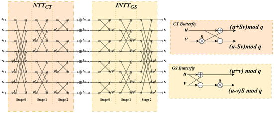
Figure 1.
Dataflow diagram for an 8-point CT-NTT (DIT) and GS-INTT (DIF). The diagram illustrates the synergistic pairing where the standard-order output of the NTT () directly feeds the standard-order input required by the INTT, eliminating the intermediate bit-reversal stage.
| Algorithm 2: INTT Algorithm based on Gentleman-Sande method |
| Require: Point-value representation A, N-point transform, Inverse N-th root of unity Ensure: Polynomial coefficients
|
3. Architectural Design
The computational demands of lattice-based post-quantum cryptography, particularly the Module-Lattice-based Key Encapsulation Mechanism, present a significant performance bottleneck for modern secure systems [11]. The core of this challenge lies in the intensive polynomial multiplication operations required for key generation, encapsulation, and decapsulation.To address this, a dedicated hardware accelerator is proposed, designed to execute the Number Theoretic Transform and its inverse with exceptional throughput and resource efficiency [12].
The architectural design is predicated on a philosophy of synergistic algorithm-hardware co-design, where algorithmic choices, microarchitectural implementation, and physical resource mapping on the Field-Programmable Gate Array (FPGA) fabric are optimized in concert [13]. This holistic approach yields a deeply pipelined, streaming dataflow architecture that achieves a superior area-time product, a critical metric for practical deployment in resource-constrained environments [14]. The fundamental design decisions and their underlying rationale are summarized in Table 1. This section provides a comprehensive exposition of the accelerator’s architecture, detailing the design of its computational core, memory subsystem, and control logic.

Table 1.
Summary of Key Architectural Design Choices and Rationale.
3.1. Design Philosophy: A Synergistic Co-Design Approach
The design of a high-performance PQC accelerator is a multi-objective optimization problem. While raw computational speed is a primary goal, practical applicability demands a careful balance between performance, resource efficiency, and flexibility [11]. The recent maturation of the PQC field, culminating in the standardization of algorithms like ML-KEM, has shifted the focus from pure proof-of-concept speed to the development of deployable, resource-aware solutions [18]. An effective accelerator must not only deliver high throughput but also be configurable for various security levels and exhibit a low area-time product to justify its hardware footprint.
This work is founded on a synergistic co-design methodology, which posits that peak efficiency is attained only when the algorithm and hardware are mutually optimized. This contrasts with a naive approach where a software-centric algorithm is merely translated into a hardware description language. Instead, every architectural decision, from the choice of the top-level NTT algorithm down to the selection of FPGA primitives for memory, is made with a clear understanding of its impact on other layers of the design. For example, the selection of the NTT/INTT algorithmic pair is made not just for mathematical correctness but for its direct impact on simplifying hardware control logic [15]. Similarly, the internal structure of the modular multiplier is pipelined specifically to match the timing characteristics of hardened DSP blocks within the FPGA fabric. This philosophy of concurrent optimization is critical for creating an accelerator that is not just fast in terms of theoretical operations per second but is holistically efficient in its use of silicon resources and its ability to sustain performance on real-world data streams.
A central challenge in this domain is the trade-off between achieving minimal latency through massive data-level parallelism and adhering to stringent resource constraints, particularly the consumption of dedicated on-chip memory blocks (BRAMs) [13]. This challenge is addressed by the proposed architecture through the integration of two core principles: a 32-way parallel streaming datapath designed to maximize throughput, and a sophisticated hybrid memory subsystem in which storage tasks are intelligently allocated between distributed logic and dedicated BRAMs to support this parallelism in a resource-efficient manner.
3.2. Overall FPGA Architecture
As depicted in the conceptual diagram of Figure 2, the proposed architecture is a modular, streaming-oriented design composed of three principal cores orchestrated by a central Control Unit (CU). The critical interaction between the Data Processing and Computation cores, which enables the high degree of parallelism, is detailed in Figure 3.
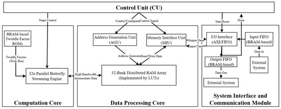
Figure 2.
Conceptual diagram of the 32-parallel streaming architecture, highlighting the hybrid memory subsystem with LUTRAM for data processing and dedicated BRAMs for constants and interface buffering.
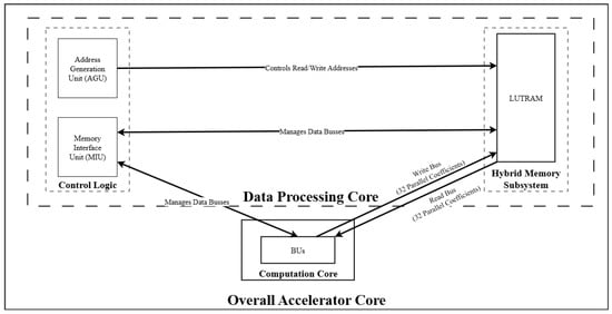
Figure 3.
High-level architectural dataflow of the proposed 32-way parallel accelerator. The system is orchestrated by the Control Logic, which houses the AGU to calculate conflict-free addresses and the MIU to manage bus arbitration. These units interact with the Hybrid Memory Subsystem, implemented using distributed LUTRAM, to provide low-latency intermediate buffering. The diagram emphasizes the high-bandwidth streaming capability, where the Computation Core utilizes a 32-coefficient wide Read Bus and Write Bus to exchange data with the memory in a single clock cycle. This parallel I/O structure, enabled by the asynchronous read capability of the LUTRAM, ensures the array of BUs remains fully utilized without pipeline stalls.
Computation Core: This core constitutes the primary computational block of the accelerator. It instantiates a 32× Parallel Butterfly Streaming Engine, processing 32 data points every clock cycle. This high degree of data-level parallelism is the cornerstone of the architecture’s low-latency performance. The engine is supplied with pre-computed constants from dedicated BRAM-based Twiddle Factor ROMs, ensuring high-speed access.
Data Processing Core: This core orchestrates the high-bandwidth data flow required to continuously feed the 32-way parallel computation engine. It is composed of a sophisticated Address Generation Unit (AGU) and a memory subsystem built upon a hybrid storage architecture. A 32-bank array of distributed RAM (LUTRAM) is utilized as a high-speed, low-latency buffer for intermediate data between the logical NTT stages. This strategic use of LUTRAM is key to the design’s resource efficiency, as it avoids the consumption of valuable BRAM for transient data storage.
System Interface and Communication Module: Seamless integration with external systems is facilitated by this module via a standard AXI/FIFO interface. Top-level control flow is managed, and dedicated BRAMs are utilized to implement robust input and output FIFO buffers. This effectively decouples the high-frequency core from the system bus and absorbs timing variations, a crucial feature for integration into complex SoC environments.
3.3. Pipelined NTT/INTT Core Architecture
The computational heart of the accelerator is a deeply pipelined NTT/INTT core structured as a streaming dataflow processor. This architecture is modeled after a Multi-Path Delay Commutator (MDC), a topology well-suited for FPGA implementations of FFT-like algorithms that require continuous data processing [14]. Unlike memory-based architectures that process data in batches, the MDC approach enables a continuous flow, where data dependencies between stages are resolved through a network of FIFOs and delay elements, eliminating stalls and maximizing hardware utilization. The core consists of a chain of eight specialized processing stages, with each stage executing one layer of the NTT/INTT decomposition. This structure is designed to accept a continuous stream of polynomial coefficients and produce a corresponding output stream after a fixed latency, achieving a throughput of 32 coefficients per clock cycle.
3.4. Unified Radix-n Butterfly Processing Element (PE)
Each stage of the pipeline is built around a butterfly Processing Element (PE), which performs the fundamental computation of the NTT/INTT. The design of this PE is a direct result of the algorithm-hardware co-design strategy.
First, a specific pairing of algorithms was selected for the forward and inverse transforms. The forward NTT is implemented using the DIT variant of the CT algorithm (Algorithm 1), while the inverse NTT employs the DIF variant of the GS algorithm (Algorithm 2) [5]. This choice is deliberate, architecturally significant, and represents a key optimization in PQC hardware. As detailed in the algorithms:
- The CT-DIT algorithm (Algorithm 1) requires its input to be in bit-reversed order and subsequently produces its output in standard (natural) order.
- Conversely, the GS-DIF algorithm (Algorithm 2) is structured to accept its input in standard order and produce its final output in bit-reversed order.
This pairing reveals the powerful hardware synergy at the heart of our architecture: the standard-order output from the CT-NTT core can be fed directly into the standard-order input of the GS-INTT core. This design choice completely obviates the need for an intermediate, resource-intensive bit-reversal permutation network that would otherwise be required between the two transforms [15]. While the complete processing chain still necessitates permutation at its external boundaries (bit-reversal on entry for the NTT and on exit from the INTT), eliminating this costly internal stage saves significant hardware resources, reduces overall latency, and dramatically simplifies the datapath.
Second, the hardware for the CT and GS butterfly operations is consolidated into a single unified butterfly unit. The arithmetic structures of the CT butterfly () and the GS butterfly () are sufficiently similar that they can be implemented with a shared set of arithmetic components [19]. The proposed PE contains one modular multiplier, one modular adder, and one modular subtractor. A single control signal, mode, configures a set of multiplexers that route data through these components to perform either the CT or GS operation. This unification strategy nearly halves the required arithmetic logic compared to implementing separate PEs for NTT and INTT, making it a key technique for achieving a low-resource footprint [14].
3.5. High-Frequency Pipelined Montgomery Modular Multiplier
In any Number Theoretic Transform (NTT) accelerator, the butterfly processing element’s performance is dominated by the modular multiplier. The goal is to compute(A × B) mod N as quickly and efficiently as possible. While several algorithms exist, the primary contenders for hardware implementation are Montgomery reduction and Barrett reduction. Both aim to replace the slow and resource-intensive trial division operation inherent in the mod operator with faster operations like multiplications and bit-shifts.
Core Principle: The Montgomery algorithm avoids division by transforming the operands into a special “Montgomery domain”. All arithmetic is performed in this domain, where modular reduction is ingeniously replaced by a series of integer multiplications, additions, and simple bit-shifts, which are extremely fast in hardware. A final conversion is required to bring the result back to the standard integer domain. Barrett reduction also avoids explicit division. It works by pre-calculating a constant based on the modulus. It then uses two integer multiplications and shifts to estimate the quotient of the division, which is then used to find the remainder.
Montgomery modules multiply hardware-centric operations, and their reliance on transformation and addition makes them highly suitable for hardware implementation. These operations are directly and effectively mapped onto digital logic, avoiding the complex control and multi-cycle delays of hardware frequency dividers. Moreover, this algorithm is most effective when performing long sequence multiplications with the same modulus, such as in the NTT calculation. The initial cost of converting an operand to a Montgomery field is averaged over many subsequent multiplications, making the entire process very fast. The iterative, step-by-step nature of the algorithm is ideal for creating a deep, balanced pipeline. This allows for a very short critical path, enabling the entire accelerator to achieve a much higher maximum clock frequency.
The advantage of Barrett is the domainless transformation. Barrett reduces the operation of standard integers and eliminates the overhead associated with entering and leaving the Montgomery field. This makes it a strong candidate for applications that only require a small amount of modular multiplication. However, the Barrett reduction step itself requires two full-width multiplications, which brings about significant delays and resource usage compared to Montgomery’s transposition-based approach. While it can be pipelined, the data dependencies involving multiple multiplications can sometimes lead to a less balanced or deeper pipeline compared to a highly optimized Montgomery architecture to achieve the same clock frequency.
Within the butterfly PE, the most critical component in terms of both area and timing is the modular multiplier. The performance of this unit dictates the maximum achievable clock frequency of the entire accelerator. The design employs the Montgomery modular multiplication algorithm, which is exceptionally well-suited for hardware implementation. Unlike standard modular multiplication that involves a computationally expensive trial division, the Montgomery method transforms operands into a special “Montgomery domain” where modular reduction is accomplished through a series of additions and simple bit-shifts, operations that map efficiently onto digital logic [20]. Therefore, through the comparison of the Montgomery model and Barrett, we ultimately chose Montgomery as the solution for our implementation.
To achieve a high operating frequency, the Montgomery algorithm is implemented as a deeply pipelined architecture [20]. The multiplication process is broken down into several sequential steps, with pipeline registers inserted between each step. This decomposition shortens the critical path within any single clock cycle, allowing the overall design to be clocked at a much higher rate than a non-pipelined or combinational implementation would allow [21]. The implementation of this pipelined multiplier is specifically tailored to leverage the dedicated DSP blocks available on modern FPGAs. These DSP blocks contain hardened, high-speed multiplier-accumulator (MAC) circuits that are significantly more area-efficient, power-efficient, and faster than synthesizing multipliers from the general-purpose LUT fabric. By structuring the Montgomery algorithm to align with the capabilities of these DSP blocks, the design achieves maximum arithmetic performance while conserving valuable logic resources.
3.6. BRAM-Efficient Streaming Memory Subsystem
In a high-throughput streaming architecture, the design of the memory subsystem is as crucial to overall performance as the computational datapath. A poorly designed memory architecture can become a major bottleneck, starving the pipeline of data and negating the benefits of a high-frequency computational core. The proposed memory subsystem is designed with a hierarchical approach, using different FPGA memory resources—namely LUTRAM and BRAM—for the tasks to which they are best suited, resulting in a system that is both high-performance and BRAM-efficient [17].
3.7. Inter-Stage Buffering with LUTRAM-Based Asynchronous FIFOs
A primary challenge in any deeply pipelined design is the transfer of data between successive pipeline stages. Each stage must receive its input data precisely when it finishes processing its previous data to avoid stalls, also known as pipeline bubbles. A common approach is to use small First-In-First-Out (FIFO) buffers to decouple the stages. However, the choice of memory resource for these FIFOs has profound performance implications.
If these FIFOs were implemented using the FPGA’s dedicated BRAM resources, a critical performance limitation would arise. BRAMs are synchronous memory blocks; they have registered outputs, meaning that a read address presented to the BRAM in clock cycle N will result in the corresponding data being available at the output in clock cycle . This inherent one-cycle read latency would introduce a mandatory one-cycle delay between every stage of the pipeline. In a streaming architecture designed for high throughput, this would force a pipeline bubble at every stage, effectively halving the accelerator’s throughput or requiring complex and resource-intensive bypass logic to manage.
To overcome this fundamental bottleneck, the inter-stage FIFOs in this architecture are implemented using LUTRAM, also known as Distributed RAM [17]. LUTRAM is synthesized from the FPGA’s general-purpose Look-Up Tables. Critically, while writes to LUTRAM are synchronous (clocked), reads are asynchronous. This means that data can be read from the memory array combinationally, without waiting for a clock edge. This property is leveraged to create a zero-latency buffer. Data produced by stage i is written into the LUTRAM FIFO at the end of a clock cycle. At the very beginning of the next clock cycle, stage can combinationally read this new data from the FIFO output. This mechanism perfectly decouples the pipeline stages without introducing any latency, allowing the pipeline to operate at its maximum theoretical throughput without stalls. This use of LUTRAM’s asynchronous read feature is a key microarchitectural optimization that enables the high-frequency, stall-free operation of the entire streaming architecture.
3.8. Twiddle Factor Storage and Management
The NTT algorithm requires a set of pre-computed constants known as twiddle factors (roots of unity) for its butterfly computations. These factors are static and are used repeatedly throughout the transformation [14]. Storing these constants off-chip in DRAM would incur an unacceptable latency penalty for each access, crippling performance. Therefore, they are stored on-chip in a Read-Only Memory (ROM).
The ideal FPGA resource for this task is the dedicated BRAM. BRAM provides a dense, power-efficient, and high-bandwidth storage solution for the relatively large dataset of twiddle factors. The access pattern for twiddle factors is highly regular and predictable, allowing for simple address generation logic to fetch the correct factor for each butterfly operation in each stage of the pipeline. By using BRAM for this bulk, static data storage, the design frees up the more flexible and latency-critical LUTRAM resources for their role as the “lubricant” of the pipeline, demonstrating an efficient and hierarchical use of the FPGA’s diverse memory capabilities.
3.9. Top-Level Integration and Control
The pipelined computational core and the specialized memory subsystem are integrated into a cohesive accelerator module managed by a centralized control unit. For seamless integration into a larger SoC design, the accelerator is equipped with industry-standard AXI-Stream interfaces for data input and output. This allows it to function as a coprocessor, receiving data streams from and returning results to a host processor, such as an embedded RISC-V core, which would manage the overall cryptographic protocol [12].
The operation of the entire accelerator is orchestrated by a top-level FSM. The FSM is responsible for managing the end-to-end dataflow and configuration of the module. Its primary tasks include:
- Initialization: Resetting the pipeline and memory pointers upon startup or new command.
- Dataflow Management: Monitoring the AXI-Stream interfaces and controlling the flow of polynomial coefficients into the first stage of the pipeline. It uses FIFO status flags (e.g., full, empty) for backpressure and flow control, ensuring no data is lost.
- Configuration Broadcasting: Driving global control signals to all PEs. This includes the mode signal to select between NTT and INTT computation, allowing the same hardware to be used for both forward and inverse transforms.
- Output Handling: Detecting when valid data emerges from the final pipeline stage and managing its transmission on the output AXI-Stream interface.
A key feature of the design is its configurability. The hardware description code is written in a parameterized fashion. This allows the same architectural template to be synthesized for different ML-KEM security levels, which are defined by the polynomial vector dimension parameter k (where or 4) [2]. By adjusting these parameters prior to synthesis, the design can be tailored to specific application requirements, enabling a direct trade-off between hardware resource utilization (area) and the level of parallelism (performance). This demonstrates a scalable and resource-aware design methodology, which is essential for deploying PQC solutions across a wide range of devices, from resource-constrained embedded systems to high-performance servers [22].
3.10. High-Parallelism Streaming Architecture and Hybrid Memory Subsystem
The achievement of an extremely low latency of 40 clock cycles with minimal dedicated memory resources (5 BRAMs) is made possible by the two synergistic design principles that define this work: a high-parallelism streaming dataflow and a hybrid memory subsystem.
3.10.1. 32-Way Parallel Streaming Model and Latency Analysis
To provide a rigorous theoretical foundation for the 40-cycle performance claim, the architecture is defined as a 32-way parallel streaming processor. For an N = 256 NTT, there are stages, each requiring 128 butterfly operations. The total latency is derived as follows:
- Core Processing Cycles per Stage: With 32 parallel butterfly units, the 128 operations per stage are completed in precisely clock cycles.
- Total Core Computation Time: For a full 8-stage NTT, the data stream requires clock cycles to traverse the entire computation core.
- Pipeline Fill Delay: The butterfly unit itself is a 5-stage pipeline. An initial 5 cycles are required to fill this pipeline before the first valid result emerges.
- {Control and Interface Overhead: A conservative 3 cycles are allocated for the top-level FSM to manage state transitions (e.g., IDLE → COMPUTE → DONE) and interface handshaking.
- Final Latency Calculation: The total latency is the sum of these components: .
This analysis confirms that the experimentally observed performance is a direct and predictable consequence of the 32-way parallel architecture.
3.10.2. The Hybrid Memory Subsystem: A Synergistic Approach
A key innovation of this architecture is the hybrid memory subsystem, which addresses the challenge of supporting 32 parallel data streams with only 5 BRAMs. This is achieved through the strategic partitioning of memory tasks between two distinct FPGA resources: distributed LUTRAM and dedicated BRAM.
The 32 parallel memory banks required for inter-stage buffering of the streaming data are implemented using LUTRAM, which is constructed from the FPGA’s general-purpose LUTs. This implementation is a deliberate architectural choice for two primary reasons:
- Right-Sized Storage and Resource Efficiency: For a 256-point transform distributed across 32 banks, each bank only needs to store coefficients. For 12-bit coefficients, this amounts to a mere 96 bits of storage per bank. Utilizing a large, 18 Kb BRAM for this purpose would result in a significant underutilization of the resource, whereas it is an ideal use case for a small number of LUTs. The resource cost of these banks is therefore correctly accounted for in the overall LUT utilization, reflecting a conscious design choice to trade abundant logic resources for scarce dedicated memory blocks.
- Performance Advantage: LUTRAM offers near-zero, asynchronous read latency, exhibiting behavior similar to that of combinatorial logic. This is critical for feeding a high-frequency, deeply pipelined computation engine, as it minimizes inter-stage data transfer bottlenecks and helps sustain the continuous data flow required to keep all 32 butterfly units fully utilized.
With the high-bandwidth intermediate storage handled by LUTRAM, the 5 reported BRAMs are strategically allocated to functions where their dedicated, high-capacity nature provides the most value. Table 2 details this allocation, demonstrating a deliberate and resource-aware design methodology.
Table 2.
BRAM Resource Allocation Scheme.
4. Experimental Results and Analysis
4.1. Implementation and Resource Utilization
To validate the proposed architecture, we targeted a Xilinx Zynq-7000 series xc7z020clg400-1 device (Xilinx, San Jose, CA, USA). The design was synthesized and implemented using the Vivado 2022.2 design suite.
The post-implementation resource utilization for the complete NTT/INTT accelerator is detailed below:
- Look-Up Tables (LUTs): 8464 (13.36% of total).
- Flip-Flops (FFs): 6673 (5.26% of total).
- Digital Signal Processor (DSP) Slices: 32 (14.55% of total).
- Block RAM (BRAM): 5 (3.57% of total).
The resource report aligns with our architectural design choices. The substantial LUT utilization is a direct consequence of implementing the 32-bank intermediate storage array using LUTRAM. The consumption of 32 DSP slices directly reflects the instantiation of 32 parallel Montgomery multipliers, which is the necessary hardware cost to achieve the 40-cycle latency. Most notably, the BRAM count is exceptionally low at just 5 blocks, validating the efficacy of our hybrid memory strategy. This demonstrates a deliberate design trade-off: leveraging a greater number of logic and DSP resources to achieve state-of-the-art latency while drastically minimizing the dependency on scarce BRAM.
4.2. Performance Evaluation
The performance of this architecture is evaluated based on two key metrics: its maximum operational frequency (), which reflects the efficiency of the pipelined datapath, and its operational latency in clock cycles, which reflects the efficiency of the parallel processing model.
Post-synthesis timing analysis, targeting a clock period of 10 ns (100 MHz), reveals a Worst Negative Slack (WNS) of 6.403 ns. This result not only confirms that timing closure was met but also indicates substantial performance headroom. The minimum achievable theoretical clock period () can be calculated as:
This corresponds to a maximum operational frequency () of:
This high frequency significantly exceeds the design target and serves as definitive proof of the architecture’s excellent timing performance, which is primarily attributable to the deep 5-stage pipelining employed throughout the design.
The total simulated latency for a complete N = 256 transform is 40 clock cycles. This experimental result is validated by a rigorous analytical breakdown of the architecture’s dataflow:
- Core Computation Time (32 cycles): An N = 256 NTT consists of stages, each requiring 128 butterfly operations. The 32-way parallel datapath executes these 128 operations in cycles per stage. The total time to process the data stream through all 8 stages is therefore clock cycles.
- Pipeline Fill Delay (5 cycles): The butterfly unit is a 5-stage pipeline. An initial latency of 5 cycles is incurred to fill this pipeline before the first valid result is produced.
- Control and Interface Overhead (3 cycles): A conservative overhead of 3 cycles is allocated for the top-level FSM to manage state transitions (e.g., IDLE → COMPUTE → DONE).
The sum of these components— cycles—perfectly aligns with the simulated latency, confirming that the 40-cycle performance is a direct and predictable consequence of the 32-way parallel architecture. At the maximum frequency of 177 MHz, this translates to an absolute latency of just 225.9 nanoseconds per transformation.
4.3. Comparison with Other Schemes
To contextualize the performance of our architecture, we provide a comparison with other state-of-the-art FPGA-based NTT implementations in Table 2. The data indicates that our design achieves an absolute execution time of 0.22 µs, establishing it as the fastest implementation among the selected works. The subsequent analysis will critically evaluate the architectural trade-offs that facilitate this performance, addressing both the advantages and inherent limitations of our approach when juxtaposed with each contemporary design.
It is important to note that the comparison in Table 3 includes implementations on disparate FPGA devices, ranging from the cost-effective Artix-7 (Xilinx, San Jose, CA, USA) and Zynq-7000 series (Xilinx, San Jose, CA, USA) to the high-performance UltraScale+ (Xilinx, San Jose, CA, USA) family. This heterogeneity is unavoidable as it reflects the specific hardware platforms chosen by the respective authors of the state-of-the-art works. While maximum frequency () and power consumption are intrinsically dependent on the semiconductor process technology (e.g., 28 nm vs. 16 nm), architectural metrics such as Cycle Count and Resource Utilization (specifically BRAM and DSP count) remain valid indicators of design efficiency across different platforms. For instance, despite the technological disadvantage of the Zynq-7000 compared to the UltraScale+ used by Waris et al. [21], our architecture achieves half the latency in clock cycles (40 vs. 80), demonstrating the architectural superiority of the proposed 32-way parallel streaming datapath independent of the underlying silicon process.
Table 3.
Performance Comparison of different FPGA Implementations.
The architecture proposed by Tian et al. [23] is noted for its remarkable resource efficiency. A principal advantage of our design lies in its superior execution speed, completing the transformation in 0.22 µs—marginally faster than the 0.24 µs achieved by Tian et al. However, a significant limitation of our approach becomes evident through this comparison: this performance gain is realized at the expense of a substantially larger hardware footprint. Our architecture consumes sixteen times more DSP slices, five times more BRAM, and nearly six times as many LUTs compared to theirs. This stark contrast underscores two divergent design philosophies; our work is clearly positioned as a high-throughput solution where performance takes precedence, and thus entails considerable resource investment as a deliberate trade-off. Conversely, Tian et al.’s design is tailored for deeply resource-constrained applications where minimal hardware footprint would be paramount—making our architecture entirely unsuitable for such scenarios.
When evaluated against the work of Lü et al. [24], our architecture demonstrates a substantial performance advantage. The execution time of 0.22 µs is nearly twice as fast as the 0.40 µs reported by Lü et al. This improvement is achieved alongside exceptional BRAM efficiency, utilizing only 5 blocks compared to their 34.5 blocks. However, a primary drawback is the doubling of DSP slice count (32 vs. 16) and a twofold increase in flip-flop utilization. This comparison validates the efficacy of our DSP-centric design philosophy over the BRAM-centric strategy employed by Lü et al. The significant gains in both speed and on-chip memory conservation present a compelling justification for increased reliance on dedicated arithmetic hardware.
Our design also exhibits considerable speed advantages over the implementation by Mandal & Roy [25], which has an execution time of 0.32 µs. This merit can be attributed to higher clock cycle efficiency; our transformation requires only 40 cycles compared to their 58 cycles at comparable maximum frequency levels. Furthermore, our architecture utilizes BRAM more economically (5 vs. 12) and LUTs more efficiently (8464 vs. 9824). A limitation within this context is a marginally higher consumption of DSP slices (32 vs. 29). Therefore, it can be concluded that our architecture possesses a superior area-time profile; it delivers significant performance enhancements with a more compact logic and memory footprint, albeit at the cost of modestly increased utilization of dedicated multipliers.
A particularly insightful comparison is drawn with the work of Waris et al. [21], which was implemented on a technologically superior Xilinx UltraScale+ device. The UltraScale+ family, based on a 16 nm process, inherently offers performance advantages over the 28 nm process utilized in the Zynq-7000 device employed in this study. Despite this significant technological disadvantage, a notable strength of our architecture lies in its faster absolute execution time (0.22 µs compared to 0.28 µs). This improvement is directly attributable to its superior cycle efficiency (40 cycles vs. 80). However, the primary limitation of our design is evident in its considerably lower maximum clock frequency (177 MHz compared to 322 MHz), which is a physical constraint imposed by the older fabrication node. Additionally, it consumes a greater number of DSP resources (32 vs. 20). These results strongly emphasize the efficiency of our architectural design, which manages to outperform an implementation on next-generation hardware while also highlighting the inherent performance ceiling associated with its target technology.
Furthermore, the design proposed by Alhassani & Benaissa [26] prioritizes minimal area over speed. In this context, the merits of our architecture are unequivocal: it operates more than three times faster (0.22 µs vs. 0.70 µs). The corresponding and necessary trade-off is that this level of performance relies on resource utilization that is an order of magnitude larger across all metrics. Their design notably lacks any DSP components; conversely, ours heavily depends upon them. It becomes clear that these two designs do not represent direct competition but rather exemplify opposite ends of the area-time design spectrum. Consequently, the substantial resource consumption associated with our work should not be viewed as a flaw but rather as a necessary and justified engineering trade-off—positioning it for high-throughput cryptographic applications where latency serves as the critical performance indicator.
4.4. Discussion and Scalability Analysis
While the experimental results validate the proposed area-time trade-off, the reliance on distributed memory and specific algorithmic parameters necessitates a rigorous evaluation of architectural robustness and scalability.
4.4.1. Timing Robustness of LUTRAM
The unpredictability of routing delays in LUTRAM-based architectures, particularly under Process, Voltage, and Temperature (PVT) variations, poses a significant challenge to timing closure compared to dedicated BRAM blocks. In the proposed design, this risk is mitigated through two primary architectural features. First, the 32-way parallelization restricts the depth of individual memory banks to merely 8 words, thereby minimizing the logic depth required for output multiplexing. Second, a substantial timing guardband is established, evidenced by the achieved Worst Negative Slack (WNS) of 6.403 ns at the 100 MHz target frequency. This margin effectively absorbs delay variances caused by PVT fluctuations, ensuring operational stability despite the utilization of general routing resources.
4.4.2. Scalability of Transform Size and Memory
The architecture is currently optimized for in alignment with ML-KEM standards, yet its extensibility is defined by distinct memory constraints.
- LUTRAM Limitations: For significantly larger transform sizes (e.g., ), timing performance is expected to be constrained by the increased fan-out and routing congestion inherent to distributed RAM interfaces. While the architecture supports scaling to or without modification, extension beyond these limits would likely necessitate the insertion of pipeline registers at LUTRAM outputs, which would require a subsequent re-balancing of the pipeline stages.
- BRAM Capacity: The design exhibits high BRAM efficiency, with the 18 Kb blocks retaining significant surplus capacity given the modest storage requirements of twiddle factors (approx. 3 Kb). Consequently, transform sizes up to or alternative moduli can be accommodated without increasing the BRAM count, as the primary constraint is port width rather than storage density.
4.4.3. Flexibility and Reuse
Although targeted at ML-KEM, the arithmetic structure of the Unified Butterfly PE is largely algorithm-agnostic. The modular adders, subtractors, and Montgomery multipliers are designed for configurability. Adaptation to alternative schemes, such as CRYSTALS-Dilithium (characterized by a distinct prime modulus), is achieved by updating the pre-computed constants in BRAM and the modulus-dependent parameters within the multiplier logic. The underlying control logic and dataflow topology remain applicable to any standard NTT/INTT-based scheme.
5. Conclusions
This paper has presented a novel NTT/INTT accelerator architecture that achieves an industry-leading 40-cycle latency with an exceptionally low BRAM footprint of only 5 blocks. This result is the direct outcome of a synergistic co-design philosophy that treats the datapath and memory subsystem as deeply intertwined components of a single, coherent strategy. We have demonstrated that it is possible to transcend the traditional trade-off between latency and BRAM utilization by pairing a massively parallel, 32-way streaming datapath with an innovative hybrid memory architecture. This architecture’s use of distributed LUTRAM for high-bandwidth transient data is the key enabler, sustaining the high throughput required by the 32 parallel DSP-based multipliers while reserving scarce BRAMs for high-value functions like constant storage and system interfaces. This work establishes a new benchmark in BRAM efficiency for high-performance PQC accelerators and provides a clear design paradigm for future work. Future work will focus on integrating this high-performance NTT/INTT core with a component-wise multiplication unit to create a complete polynomial multiplier and exploring its application within a full ML-KEM cryptographic processor.
Author Contributions
Conceptualization, X.G. and X.L.; Methodology, Y.L.; Software, Y.L. and T.L.; Validation, Y.L., T.L. and X.L.; Formal analysis, X.G., X.L. and J.W.; Investigation, Y.L.; Resources, X.G., X.L. and J.W.; Data curation, Y.L.; Writing—original draft preparation, Y.L.; Writing—review and editing, X.G. and T.L.; Visualization, T.L.; Supervision, X.G., X.L. and J.W.; Project administration, X.G. and J.W.; Funding acquisition, X.G. and J.W. All authors have read and agreed to the published version of the manuscript.
Funding
This work was supported in part by the Fundamental Research Funds for the Central Universities under Grant 3282023009 and 3282024057.
Data Availability Statement
Data are contained within the article.
Conflicts of Interest
The authors declare no conflicts of interest. The funders had no role in the design of the study; in the collection, analyses, or interpretation of data; in the writing of the manuscript; or in the decision to publish the results.
References
- Shor, P.W. Algorithms for quantum computation: Discrete logarithms and factoring. In Proceedings of the 35th Annual Symposium on Foundations of Computer Science (FOCS 1994), Santa Fe, NM, USA, 20–22 November 1994; IEEE: Piscataway, NJ, USA, 1994; pp. 124–134. [Google Scholar] [CrossRef]
- National Institute of Standards and Technology. Module-Lattice-Based Key-Encapsulation Mechanism Standard (FIPS 203); U.S. Department of Commerce: Gaithersburg, MD, USA, 2024. [Google Scholar] [CrossRef]
- NIST Releases First 3 Finalized Post-Quantum Encryption Standards. Available online: https://www.nist.gov/news-events/news/2024/08/nist-releases-first-3-finalized-post-quantum-encryption-standards (accessed on 4 September 2025).
- Cooley, J.W.; Tukey, J.W. An algorithm for the machine calculation of complex Fourier series. Math. Comput. 1965, 19, 297–301. [Google Scholar] [CrossRef]
- Gentleman, W.M.; Sande, G. Fast Fourier transforms: For fun and profit. In Proceedings of the 7–10 November 1966, Fall Joint Computer Conference, San Francisco, CA, USA, 7–10 November 1966; ACM: New York, NY, USA, 1966; pp. 563–578. [Google Scholar] [CrossRef]
- Gandelman, S.P.; Niu, M.; Hileman, M.; Wilkens, S.; Spencer, M.; Gauthier, D.J.; Plante, G. Hands-On Quantum Cryptography: Experimentation with the B92 Protocol Using Pulsed Lasers. Photonics 2025, 12, 220. [Google Scholar] [CrossRef]
- Srisiri, G.; King, B.; Vappangi, S. Deep Learning-Based Channel Estimation for Continuous Variable Quantum Cryptography in Free-Space Optical (FSO) Communication. In Proceedings of the 2025 6th International Conference on Inventive Research in Computing Applications (ICIRCA), Coimbatore, India, 25–27 June 2025; IEEE: Piscataway, NJ, USA, 2025. [Google Scholar]
- Bos, J.; Ducas, L.; Kiltz, E.; Lepoint, T.; Lyubashevsky, V.; Schanck, J.M.; Schwabe, P.; Seiler, G.; Stehlé, D. CRYSTALS–Kyber: A CCA-secure module-lattice-based KEM. In Proceedings of the 2018 IEEE European Symposium on Security and Privacy (EuroS&P), London, UK, 23–27 April 2018; IEEE: Piscataway, NJ, USA, 2018; pp. 353–367. [Google Scholar] [CrossRef]
- Mao, G.; Chen, D.; Li, G.; Dai, W.; Sanka, A.I.; Koç, Ç.K.; Cheung, R.C.C. High-performance and configurable SW/HW co-design of post-quantum signature CRYSTALS-Dilithium. ACM Trans. Reconfig. Technol. Syst. 2023, 16, 1–28. [Google Scholar] [CrossRef]
- Pöppelmann, T.; Güneysu, T. Towards efficient and secure lattice-based cryptography on 8-bit microcontrollers. In Smart Card Research and Advanced Applications; Mangard, S., Ed.; Springer: Berlin/Heidelberg, Germany, 2012; pp. 29–44. [Google Scholar] [CrossRef]
- Di Matteo, S.; Sarno, I.; Saponara, S. CRYPHTOR: A Memory-Unified NTT-Based Hardware Accelerator for Post-Quantum CRYSTALS Algorithms. IEEE Access 2024, 12, 11356–11375. [Google Scholar] [CrossRef]
- He, P.; Bao, T.; Xie, J.; Amin, M. FPGA Implementation of Compact Hardware Accelerators for Ring-Binary-LWE-based Post-quantum Cryptography. ACM Trans. Reconfig. Technol. Syst. 2023, 16, 45. [Google Scholar] [CrossRef]
- Petri, R. Lightweight Software-Hardware Codesign for Post-Quantum Cryptography. Ph.D. Thesis, University of Southern Denmark, Odense, Denmark, 2025. [Google Scholar] [CrossRef]
- Imran, M.; Khalid, A.; Rafferty, C.; Rashid, M.; O’Neill, M. Evaluating area-time-power trade-offs in NTT accelerators for post-quantum cryptography. In Proceedings of the 2025 IEEE International System-on-Chip Conference (SOCC), Dubai, United Arab Emirates, 29 September–1 October 2025; IEEE: Piscataway, NJ, USA, 2025. [Google Scholar]
- Rashid, M.; Sonbul, O.S.; Jamal, S.S.; Jaffar, A.Y.; Kakhorov, A. A Pipelined Hardware Design of FNTT and INTT of CRYSTALS-Kyber PQC Algorithm. Information 2024, 16, 17. [Google Scholar] [CrossRef]
- Mondal, A.; Ghosh, S.; Das, A.; Chowdhury, D.R. Efficient FPGA Implementation of Montgomery Multiplier Using DSP Blocks. In Progress in VLSI Design and Test. Lecture Notes in Computer Science; Rahaman, H., Chattopadhyay, S., Eds.; Springer: Berlin/Heidelberg, Germany, 2012; Volume 7373. [Google Scholar] [CrossRef]
- Ni, Z.; Khalid, A.; Liu, W.; O’Neill, M. Towards a lightweight CRYSTALS-Kyber in FPGAs: An ultra-lightweight BRAM-free NTT core. In Proceedings of the 2023 IEEE International Symposium on Circuits and Systems (ISCAS), Monterey, CA, USA, 21–25 May 2023; IEEE: Piscataway, NJ, USA, 2023; pp. 1–5. [Google Scholar] [CrossRef]
- National Institute of Standards and Technology. Post-Quantum Cryptography. Available online: https://csrc.nist.gov/projects/post-quantum-cryptography (accessed on 1 November 2025).
- Kundi, D.E.S.; Bermudo Mera, J.M.; Strub, P.-Y.; Hutter, M. High-Performance NTT Hardware Accelerator to Support ML-KEM and ML-DSA. In Proceedings of the 2024 Workshop on Attacks and Solutions in Hardware Security (ASHES ’24), Salt Lake City, UT, USA, 14–18 October 2024; ACM: New York, NY, USA, 2024; pp. 100–105. [Google Scholar] [CrossRef]
- Montgomery, P.L. Modular multiplication without trial division. Math. Comput. 1985, 44, 519–521. [Google Scholar] [CrossRef]
- Waris, A.; Aziz, A.; Khan, B.M. Area-time efficient pipelined number theoretic transform for CRYSTALS-Kyber. PLoS ONE 2025, 20, e0323224. [Google Scholar] [CrossRef] [PubMed]
- Mu, J.; Wang, Y.R.; Hu, Y.; Chen, S.; Chang, C.-H. Scalable and Conflict-Free NTT Hardware Accelerator Design: Methodology, Proof, and Implementation. IEEE Trans.-Comput.-Aided Des. Integr. Circuits Syst. 2023, 42, 1504–1517. [Google Scholar] [CrossRef]
- Tian, H.; Wang, X.; Zhang, H. FPGA design optimization based on post-quantum cryptography improvement algorithm. Adhesion 2025, 52, 155–157. [Google Scholar] [CrossRef]
- Lü, S.S.; Li, B.; Zhai, J.Q.; Li, S.Q.; Zhou, Q.L. FPGA efficient parallel optimization of Crystal-Kyber. Acta Electron. Sin. 2024, 52, 1679–1689. [Google Scholar] [CrossRef]
- Mandal, S.; Roy, D.B. Winograd for NTT: A case study on higher-radix and low-latency implementation of NTT for post-quantum cryptography on FPGA. IEEE Trans. Circuits Syst. I Regul. Pap. 2024, 71, 6396–6409. [Google Scholar] [CrossRef]
- Alhassani, A.; Benaissa, M. High-speed polynomials multiplication HW accelerator for CRYSTALS-Kyber. IEEE Trans. Circuits Syst. I Regul. Pap. 2024, 71, 6105–6113. [Google Scholar] [CrossRef]
Disclaimer/Publisher’s Note: The statements, opinions and data contained in all publications are solely those of the individual author(s) and contributor(s) and not of MDPI and/or the editor(s). MDPI and/or the editor(s) disclaim responsibility for any injury to people or property resulting from any ideas, methods, instructions or products referred to in the content. |
© 2025 by the authors. Licensee MDPI, Basel, Switzerland. This article is an open access article distributed under the terms and conditions of the Creative Commons Attribution (CC BY) license (https://creativecommons.org/licenses/by/4.0/).