Abstract
This article presents the analysis of the electromagnetic (EM) properties of a novel metamaterial (MM) array in the microwave frequency range. The background for this work is the rapid development of portable devices with low individual energy consumption for the so-called “Internet of Things” (IoT) and the demand for energy harvesting from the environment on a micro scale through harvesters capable of powering billions of small receivers globally. The main goal of this work was to check the potential of the novel MM array structure for EM energy harvesting. The proposed MM array was analyzed in the CST Studio simulation environment. This resulted in the determination of the substitute average EM parameters (absorption, reflection, and transmission) of the MM array. Then, the MM array was manufactured, and the simulation results of the MM array parameters were experimentally validated in a microwave waveguide test system. Based on this conclusion, a prototype of the microwave MM absorber, together with an RF/DC converter, was designed and manufactured for harvesting EM energy from the environment. The system’s energy efficiency was evaluated, and its potential application in energy harvesting technology was appraised. Using a microwave horn antenna, the EM energy harvesting efficiency of the prototype was evaluated. It was about 50% at a microwave frequency of about 2.6 GHz. This may make the prototype attractive as an EM energy harvester or bolometric sensor.
1. Introduction
Technological progress and the exponentially growing number of mobile electronic devices are causing an increase in the demand for electrical energy worldwide. While individual electronic devices have relatively low energy demands (wearable devices, Internet of Things), the dynamic growth in their quantity necessitates the exploration of new alternative energy sources to power them. Addressing this need is the technology of Wireless Power Transfer (WPT), which utilizes various forms of energy present in the environment, ranging from solar and thermal energy to the kinetic energy of acoustic waves and the energy of electromagnetic (EM) waves. WPT encompasses elements, devices, and systems that operate by harnessing energy from the surroundings, known as Ambient Energy Harvesting (AEH) [1]. Environmental energy sources can include devices and systems using EM radiation for communication, such as mobile phones, GSM system antennas, WiFi routers, Bluetooth headphones, and more. It is expected that in the era of the development of the Internet of Things (IoT) and smart cities, the energy of radio and microwave waves generated in the environment in a wide frequency range will become ubiquitous, and devices with low energy demand will be able to obtain RF energy and MW wirelessly in a continuous way. It is believed that obtaining RF and MW energy from the environment is becoming a trend in the development of low-power wireless energy transfer systems.
To assess the energy potential and identify the most favorable frequency ranges for EM Energy Harvesting applications, a study was conducted to examine the frequency spectrum of microwave power density averaged over a 20 min period.
Figure 1 illustrates the spectrum power distribution of the EM field in terms of frequency on the campus of Gdynia Maritime University, Gdynia, Poland (Figure 1). The spectrum depicted in Figure 1 indicates that within the campus environment, the highest values of EM field power correspond to the frequencies used by wireless communication systems such as DTV, DVB-C, GSM, and LTE/WiFi [2].
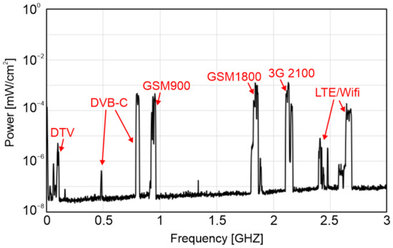
Figure 1.
Spectrum of the power distribution of the EM field in the vicinity of Gdynia Maritime University, Gdynia, Poland.
The ubiquity of EM energy sources in the environment represents a significant energy potential that can be harnessed in WPT technology. In recent years, there has been increased interest in new materials for their suitability as absorptive elements for EM radiation. The exploration of new absorptive materials focuses particularly on so-called EM metamaterials (MM), whose unconventional EM properties are not widely known and practically utilized.
Electromagnetic metamaterials are unconventional materials with extraordinary EM properties. MM structures can exist in two-dimensional forms or in three-dimensional forms, with various spatial geometries. Metamaterials are constructed from structural units known as MM unit cells. These unit cells serve as the building blocks from which larger metamaterial structures are fashioned, both as metasurfaces (2D) and various spatial geometries (3D).
The EM properties of MM structures depend on the shape of their individual components, material parameters, the frequency of incident radiation, and the ratio of the characteristic dimension of an MM unit cell to the wavelength of the incident EM wave. The metamaterial effect is observed when the size of the MM unit cell is considerably smaller than the wavelength of the electromagnetic (EM) wave it interacts with. Metamaterials exhibit exceptional characteristics, such as a negative refractive index, the inverse Doppler effect, the reversal of the group and phase velocity vectors of the wave, and an augmentation of the electromagnetic wavelength as the frequency increases. Thanks to these characteristics, metamaterials can block, absorb, enhance, or bend electromagnetic waves and have significant potential applications in various scientific and technological fields.
Based on their operating frequency, EM MM structures can be categorized as terahertz, optical, and microwave [3]. Terahertz metamaterials are designed to interact with electromagnetic waves in the terahertz (THz) frequency range, which typically spans from 0.1 to 10 THz. This range is situated between microwave and infrared frequencies. Optical metamaterials are engineered to manipulate light in the visible and near-infrared spectrum, encompassing frequencies from hundreds of terahertz to hundreds of petahertz (PHz). Microwave metamaterials operate within the microwave frequency range, typically spanning from hundreds of megahertz (MHz) to tens of gigahertz (GHz). Each category serves specific purposes and applications, harnessing the unique EM properties of MM to manipulate and control waves in their respective frequency ranges. A very popular category of EM metamaterials is microwave metamaterials [3].
Due to the EM properties, EM metamaterials are divided into resonant and non-resonant categories. Resonant metamaterials typically consist of metal loops with gaps. Their properties generally result from the macroscopic interaction of the arrangement of loops and gaps with incident EM radiation. On the other hand, the properties of non-resonant metamaterials result from interactions of their microscopic structure with incident EM radiation [3]. Resonant metamaterials are the most popular group of metamaterials.
The operation of a MM structure is based on the magnetic resonance, which arises from the resonant LC circuit formed by the capacitance of the gap and the inductance of the metal loop. The charges accumulated in the gap capacitance during the interaction of the MM structure with the incident EM radiation can be utilized by placing a load, e.g., a resistor, in the gap. The voltage obtained in this way can be used to power low-power electronic devices, such as GPS and RF receivers, hearing aids, RFID systems, etc.
Among the most popular application examples of EM metamaterials are antenna metamaterials (improving and increasing the efficiency of antenna systems while maintaining small sizes) [3], superlenses (achieving resolution beyond the diffraction limit) [4], and camouflage devices (manipulating light beams) [5].
The use of metamaterials in electromagnetic energy harvesting systems is the subject of many studies [6,7,8,9]. Their undeniable advantages, including low production costs, simple construction, and the availability of materials used in their manufacturing, make them attractive structures for research, with potential practical implementation. Although some MM structures exhibit a high absorption efficiency with regard to EM radiation (of the order of 80% [10,11,12,13]), new MM structures are under study [10,11,12,13]. Another challenge MM harvesting technology faces is an unsatisfactory efficiency in converting the absorbed EM energy by MM structures into electrical energy by RF/DC converters (less than 50% [14,15,16]). Considering the limited resources of EM energy in the environment, the apparent goal is to achieve the highest possible efficiency in converting EM energy into electrical energy. Attaining higher efficiency translates into broader potential applications of metamaterial structures.
This work first aims to check if the proposed novel MM array structure is suitable for EM energy harvesting in the microwave frequency range. For this purpose, numerical simulation studies of the EM parameters (absorption reflection and transmission) of the novel MM array structure in the microwave range were performed. Next, the simulation results were experimentally validated using a microwave antenna system. Then, based on these results, a microwave prototype for EM energy harvesting using the MM array with a dedicated RF/DC converter was proposed and manufactured. Finally, the EM harvesting ability of the microwave prototype for EM energy harvesting was tested by measuring the efficiency in converting the absorbed EM energy by the novel MM array structure into electrical energy by the dedicated RF/DC converter.
2. Selected Microwave Metamaterial Array
Microwave metamaterials come in various geometries, with planar two-dimensional array metasurfaces being the most common. These planar arrays consist of MM unit cells. The characteristic dimension of a single structure is smaller than one-fourth of the wavelength of the incident EM wave [17,18]. The dimensions of MM structures designed to operate in the microwave frequency range are typically in the order of single centimeters. Planar MM arrays can form symmetric or asymmetric arrays [19]. They can also be arranged into three-dimensional structures [18].
As mentioned above, the metamaterials are divided into resonant and non-resonant categories. The resonant metamaterials, exhibiting higher efficiency in this range, are easier to implement in the microwave range [20,21,22]. Among the most well-known resonant MM structures in the microwave range are split-ring resonators (SRRs) [23], characterized by a relatively narrow resonance band and high absorptive capacity [24,25]. Other resonant structures include Electric LC Circuit (ELC) structures [25,26,27,28] and spiral structures [22], although their popularity in the microwave range is lower compared to the SRR structures. The planar MM array presented in this paper is a resonant MM structure, suitable for use in the microwave range.
The planar MM arrays are composed of mosaics consisting of metallic pathways and “void” areas (gaps) between them. The mosaics are placed on dielectric plates. The metallic traces form an electric inductance, while the gaps between the traces are an electric condenser. Both constitute the resonant LC circuit. When the planar MM array interacts with EM radiation, the electric charges accumulate in the gap regions. The resulting potential difference in the gap can be utilized as a “source” of voltage. This voltage can be practically applied in the harvesting process.
The MM array proposed as a resonant microwave planar metamaterial consists of single MM unit cells (Figure 2) arranged in two rows and three columns (Figure 3), forming a 2 × 3 MM array. An arrangement of each single unit cell consists of copper traces with a thickness of 35 µm, superimposed on a rectangular dielectric substrate (FR-4). Behind the substrate is a metallic layer with a thickness of 35 µm, serving as an EM shield (a reflector).
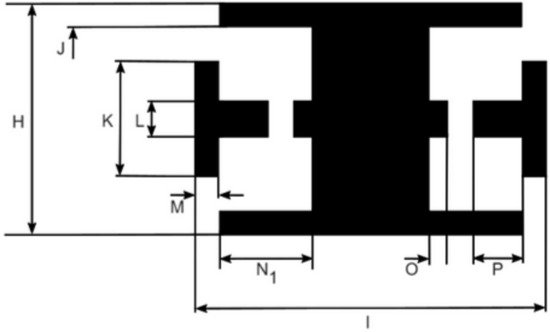
Figure 2.
The geometry of the single MM unit cell. Dimensions marked with letters are summarized in Table 1.
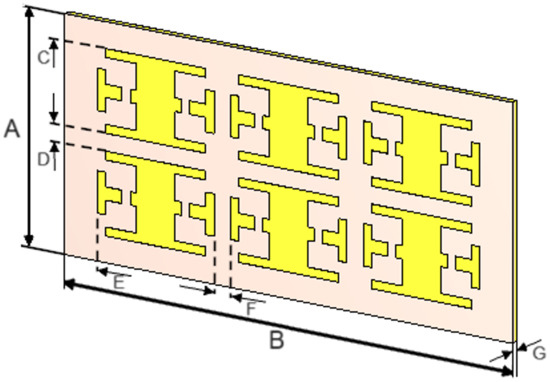
Figure 3.
The geometry of the investigated planar MM array, consisting of 6 single MM unit cells placed on the FR-4 dielectric substrate. Dimensions marked with letters are summarized in Table 1.
The mosaic arrangement of the copper traces in the MM unit cell (Figure 2) enables the resonant frequency of the single MM unit cell to be changed in many ways by altering the dimensions of length and width and the distances between the traces.
The EM properties of the proposed resonant microwave MM structure were preliminarily investigated by the authors in simulation and experimental tests (described in [29]). The obtained results indicated that this structure exhibits strong absorption properties.
In the present work, apart from designing the proposed MM array to resonate around a frequency of 2.6 GHz and simulating and experimentally studying its EM properties within this frequency range, investigations were conducted on the suitability of the proposed MM array for harvesting EM energy from the EM environment.
The dimensions of copper traces in a single MM unit cell, as well as the distances between unit cells in the MM array, were optimized to achieve the maximum absorption of the EM radiation at a frequency of approximately 2.6 GHz. The dimensions of a single MM unit cell were selected based on the wavelength corresponding to a frequency of 2.6 GHz in such a way that the characteristic dimension of this unit cell does not exceed one-fourth of the wavelength of the incident EM wave. The frequency value was selected based on the characteristics of the EM smog spectral power density in the 9 kHz to 2.7 GHz band in an urban environment in Poland [30]. The dimensions of the MM array and the single MM unit cell are summarized in Table 1.

Table 1.
The dimensions of the MM array and the single MM unit cell.
3. Simulation and Experimental Studies of the Metamaterial Array
The numerical simulation of the microwave MM array was performed using CST Studio 2019 software. The software enables modeling and comprehensive simulations of high-frequency EM fields for 3D objects [31]. This environment uses the Finite Element Method (FEM) and Method of Moments (MoM) in the frequency domain to solve EM field problems.
The simulation consisted of performing numerical calculations using the Frequency Solver. This tool enables obtaining the array response for a sinusoidal signal (EM radiation) of a specific frequency. Ultimately, it becomes feasible to find the array response in the chosen frequency range.
The EM radiation propagates in the −z direction, implying boundary conditions in the CST Studio 2019 software package. A perfect electric conductor boundary condition (Figure 4, Et = 0) is assumed along the walls of the x-axis and the y-axis
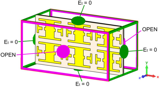
Figure 4.
Virtual waveguide with the propagation path and boundary conditions. The direction of the EM radiation propagation is towards the −z direction.
The simulation procedure involved placing the investigated metamaterial array in a virtual waveguide for the EM radiation (Figure 4).
In general, the EM radiation incident on the MM array can be absorbed, reflected, and transmitted by the structure. In the CST Studio 2019 software, which simulates the processes of absorption, reflection, and transmission, the coefficients of the so-called scattering matrix S for the incident radiation on the studied structure are determined [32]. Knowing the values of the scattering matrix coefficients S11, S12, S21, and S22, as functions of frequency, it is possible to calculate the frequency characteristics of the absorption A, reflection R, and transmission T coefficients of the studied MM array [33]. The simulation was carried out in the frequency range from 2 to 3 GHz.
The experimental investigations of the EM properties (absorption, reflection, and transmission coefficients) of the planar MM array were carried out using the waveguide techniques with the use of a vector network analyzer (VNA) (Figure 5). The measuring test system consisted of a VNA Keysight N5225, between the input and output of which the measurement path was connected via coaxial cables and adapters. The measurement path was composed of two WR-430 waveguides, in which the investigated MM array was placed.
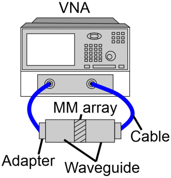
Figure 5.
Schematic diagram of the test system using the waveguide techniques with VNA.
The MM array for the experimental measurements was manufactured using the photochemical etching method on printed circuit boards. For this purpose, double-sided (three-layer) printed circuit boards consisting of FR-4 dielectric covered on both sides with a copper layer of 35 µm thickness were employed. The dimensions of the MM array were like those of the MM array used in the simulation.
Figure 6, Figure 7 and Figure 8 show the simulated (using CST) and measured (with the waveguide techniques) frequency characteristics of the absorption A, reflection R, and transmission T coefficients of the MM array in the frequency range of 2 to 3 GHz. The values of the coefficients must satisfy the equation A + R + T = 1.
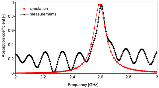
Figure 6.
Absorption A coefficient of the EM radiation by the MM array as a function of frequency.
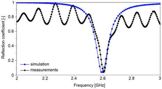
Figure 7.
Reflection R coefficient of the EM radiation by the MM array as a function of frequency.
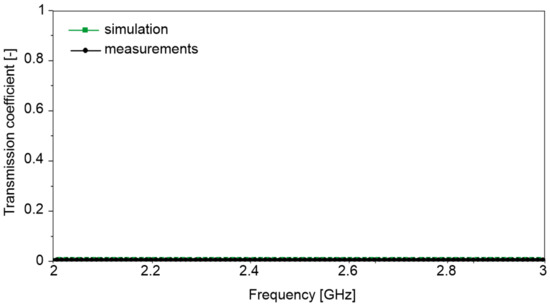
Figure 8.
Transmission T coefficient of the EM radiation by the MM array as a function of frequency.
The frequency characteristics of the absorption A, reflection R, and transmission T coefficients obtained from the numerical simulation and experimental studies showed that the examined MM array exhibits strong absorption properties for microwave radiation. The absorption properties of the MM array have a resonant character. The simulation studies showed that the absorption coefficient of the MM array reaches its maximum (A = 96%) at resonant frequency f = 2.596 GHz. The experimental research results are consistent with the simulation ones. The experimental absorption coefficient reaches its maximum value, A = 95.9%, at a frequency of f = 2.606 GHz. This positively validates the applied simulation method. The transmission coefficient T of the studied MM array in the whole frequency range is zero due to the metallic layer at the rear side of the array serving as the EM shield. The wavy form of the A and R characteristics at frequencies beyond the resonant frequency results from the zero transmission of the MM array and the formation of a standing wave in the waveguide, which is monitored by the vector network analyzer.
We found that the resonant frequency of the MM array could easily be changed by altering the dimensions of length and width and the distances of the copper traces in the single MM unit cell. For example, by increasing the parameter N1 in the single MM unit cell (Figure 2) by 1 mm, the resonant MM array frequency decreased by 0.1 GHz.
4. A Prototype for EM Energy Harvesting Using the Metamaterial Array
To assess the suitability of the MM arrays for EM energy harvesting applications, a prototype system was developed for converting the EM energy absorbed by the MM array from the EM field into useful DC power. The prototype consists of an MM array and an RF/DC converter (Figure 9). To assemble the EM harvesting system, we attached an SMA (f) connector to the output of the constructed metamaterial array. Similarly, for the input of the RF/DC converter, we connected an SMA (m) connector.
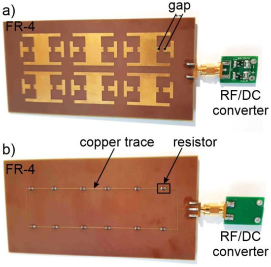
Figure 9.
The MM array prototype with resistors placed on the backside and the RF/DC converter for the EM harvesting system: front and rear view. (a) Front view: an example a gap where the resistor is inserted. (b) Rear view: resistors connected in series on the back side of FR-4 plate.
The experimental setup for testing the harvesting ability of the prototype consisted of a microwave signal generator that supplied a horn antenna, the MM array, and the RF/DC converter (Figure 10).
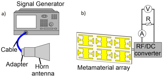
Figure 10.
The experimental setup for testing the energy harvesting system, consisting of the antenna (a) and the MM absorber prototype with the RF/DC converter (b).
In the test, an EM signal of variable frequency from a signal generator Keysight N5181B (9 kHz to 6 GHz) was delivered to a broadband horn antenna (1700 MHz to 2600 MHz); see Figure 10. Then, the horn antenna emitted the EM radiation towards the MM array. The surface power density radiated by the antenna with an aperture of 3169 cm2 (dimensions of the antenna aperture: 61 cm × 51 cm) towards the MM array was 3.8 mW/m2. The energy of EM radiation incident on the MM array accumulated in the gap regions of each single MM unit cell in the form of the electrical voltage, which could be transferred to the RF/DC converter using resistors inserted in the gaps, connected in series (Figure 9).
The aim of the experimental test was to measure the electrical voltage, current, and power at the converter output and finally determine the energy conversion efficiency of the prototype.
The prototype MM array was fabricated using the photochemical etching method on printed circuit boards. To manufacture the prototype, a four-layer printed circuit board was used. The first layer consisted of six single MM unit cells made of copper. The second layer was an FR-4 dielectric. An EM shield (a copper layer) formed the third layer. The fourth layer was composed of an FR-4 dielectric plate, with copper traces connecting resistors inserted in the gaps. Figure 9 depicts the MM array with resistors inserted in the gaps and the RF/DC converter for EM energy harvesting.
The RF/DC converter was built with the use of high-frequency Schottky diodes and capacitors with a capacitance of 1 nF and 10 nF. The optimal value of the resistors placed in the single MM unit cell gaps was experimentally found to be 3 kΩ (Figure 11).
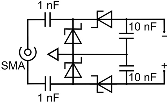
Figure 11.
Electric circuit of the RF/DC converter for microwave energy harvesting presented in Figure 12.
To achieve matching of the MM array with measurement instruments and find the maximum voltage and current, at the output of the RF/DC converter circuit, a resistor decade was connected to the output. The voltage, current, and the output power at the RF/DC converter output were measured. The maximum value of the output power was approximately 60 µW at a voltage of 2 V and current of 30 µA. Measuring the EM power from the horn antenna incident on the MM array, the maximum value of energy conversion efficiency of the MM prototype with the RF/DC converter was estimated at a level of approximately 50% for the frequency of 2.59 GHz. The manufactured prototype of an RF/DC converter is shown in Figure 12. To connect the harvesting system, we attached an SMA (f) connector to the output of the constructed metamaterial array. Additionally, for the input of the RF/DC converter, we connected an SMA (m) connector. Figure 12 provides a clearer explanation and additional description.
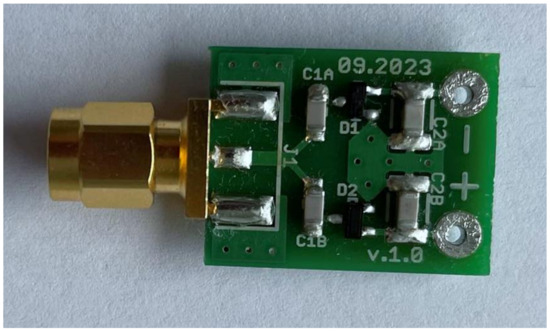
Figure 12.
The prototype of an RF/DC converter with SMA connector.
5. Summary and Conclusions
A planar MM array of original design, consisting of six single MM unit cells, was presented. Its EM parameters (absorption, reflection, and transmission) were determined by numerical simulation using CST Studio. The results obtained were validated using the microwave waveguide technique. The validation confirmed the simulation results, showing strong resonant absorption (96%) of the planar MM array at a frequency of around 2.6 GHz. The resonant frequency can easily be tuned by altering the dimensions of length and width and the distances between the traces in the single MM unit cell.
Based on these results, the microwave prototype for EM energy harvesting using the MM array with an RF/DC converter was proposed, manufactured, and tested. The efficiency of energy transmission to the receiver or potential energy storage reaches a value of approximately 50%. Such an efficiency may be attractive. The proposed prototype of the EM harvesting system can power low-power devices with an energy demand below 0.1 mW (e.g., hearing aids, RFIDS systems, watches, calculators, quartz clocks). Also, the modified prototype may be interesting as an EM bolometric sensor.
The attractive findings obtained motivate us to plan further work on developing the proposed MM array structure and RF/DC converter. So far, we have checked the operation of the proposed MM array structure as a single-band absorber having a near-unity absorption coefficient with zero reflection and transmission at a selected frequency from the frequency bands used by microwave wireless communication systems, which are the strongest sources of EM energy in our neighborhood. It should also be checked whether the modified MM array will demonstrate high absorption of EM radiation simultaneously in several frequency bands. In particular, in those bands that we find in our environment. It seems that the unique geometry of the design of the proposed MM array makes this a possibility. Widening the bandwidth of our MM array structure would increase its total absorption and harvesting abilities. It should also be examined whether the proposed MM array is polarization-sensitive. Polarization-insensitive MM arrays operating as multi-band absorbers find applications in Radar cross-section reduction (RDS), EM energy harvesting, EM shielding, and EM sensors.
Author Contributions
Conceptualization, M.B. and J.M.; methodology, M.B. and J.M.; investigation, M.B. and J.M.; writing—original draft preparation, M.B. and J.M.; writing—review and editing M.B. and J.M.; visualization, M.B. and J.M.; supervision, M.B. and J.M. All authors have read and agreed to the published version of the manuscript.
Funding
This research received no external funding.
Data Availability Statement
Data are contained within the article.
Conflicts of Interest
The authors declare no conflicts of interest.
References
- Capolino, F. Applications of Metamaterials; CRC Press: Boca Raton, FL, USA, 2009. [Google Scholar]
- Budnarowska, M.; Mizeraczyk, J. The numerical simulation of the interaction of a plane electromagnetic wave with a metasurface consisting of split-ring resonator, (in Polish: Oddziaływanie płaskiej fali elektromagnetycznej z metapowierzchnią złożoną z rezonatorów SRR 2,5 GHz). Przegląd Elektrotechniczny 2021, 97, 39–42. [Google Scholar]
- Mendhe, S.E.; Kosta, Y.P. Metamaterial properties and applications. Int. J. Inf. Technol. Knowl. Manag. 2011, 4, 85–89. [Google Scholar]
- Pendry, J.B. Negative refraction makes a perfect lens. Phys. Rev. Lett. 2000, 85, 3966. [Google Scholar] [CrossRef] [PubMed]
- Oliveri, G.; Werner, D.H.; Massa, A. Reconfigurable electromagnetics through metamaterials—A review. Proc. IEEE 2015, 103, 1034–1056. [Google Scholar] [CrossRef]
- Tran, L.G.; Cha, H.K.; Park, W.T. RF power harvesting: A review on designing methodologies and applications. Micro Nano Syst. Lett. 2017, 5, 1–16. [Google Scholar] [CrossRef]
- Aldhaeebi, M.A.; Almoneef, T.S. Planar dual polarized metasurface array for microwave energy harvesting. Electronics 2020, 9, 1985. [Google Scholar] [CrossRef]
- Amer, A.G.; Othman, N.; Sapuan, S.Z.; Alphones, A.; Salem, A.A. High-efficiency electromagnetic energy harvesting using double-elliptical metasurface resonators. PLoS ONE 2023, 18, e0291354. [Google Scholar] [CrossRef]
- Sim, M.S.; You, K.Y.; Esa, F.; Hamid, F. Metamaterials and Metasurfaces for Radio-Frequency Energy Harvesting Applications. In Metamaterial Technology and Intelligent Metasurfaces for Wireless Communication Systems; IGI Global: Hershey, PA, USA, 2023; pp. 270–296. [Google Scholar]
- Hu, W.; Yang, Z.; Zhao, F.; Wen, G.; Li, J.; Huang, Y.; Inserra, D.; Chen, Z. Low-cost air gap metasurface structure for high absorption efficiency energy harvesting. Int. J. Antennas Propag. 2019, 2019, 1727619. [Google Scholar] [CrossRef]
- Ghaneizadeh, A.; Mafinezhad, K.; Joodaki, M. Design and fabrication of a 2D-isotropic flexible ultra-thin metasurface for ambient electromagnetic energy harvesting. AIP Adv. 2019, 9, 025304. [Google Scholar] [CrossRef]
- Zhang, X.; Liu, H.; Li, L. Electromagnetic power harvester using wide-angle and polarization-insensitive metasurfaces. Appl. Sci. 2018, 8, 497. [Google Scholar] [CrossRef]
- Duan, X.; Chen, X.; Zhou, Y.; Zhou, L.; Hao, S. Wideband metamaterial electromagnetic energy harvester with high capture efficiency and wide incident angle. IEEE Antennas Wirel. Propag. Lett. 2019, 17, 1617–1621. [Google Scholar] [CrossRef]
- Chandrasekaran, K.T.; Agarwal, K.; Alphones, A.; Mittra, R.; Karim, M.F. Compact dual-band metamaterial-based high-efficiency rectenna: An application for ambient electromagnetic energy harvesting. IEEE Antennas Propag. Mag. 2020, 62, 18–29. [Google Scholar] [CrossRef]
- Almoneef, T.S.; Erkmen, F.; Ramahi, O. Harvesting the energy of multi-polarized electromagnetic waves. Sci. Rep. 2017, 7, 14656. [Google Scholar] [CrossRef]
- Duan, X.; Chen, X.; Zhou, L. A metamaterial harvester with integrated rectifying functionality. In Proceedings of the 2016 IEEE/ACES International Conference on Wireless Information Technology and Systems (ICWITS) and Applied Computational Electromagnetics (ACES), Honolulu, HI, USA, 13–18 March 2016; IEEE: Piscataway, NJ, USA; pp. 1–2. [Google Scholar]
- Slyusar, V.I. Metamaterials on antenna solutions. In Proceedings of the International Conference on Antenna Theory and Techniques, Lviv, Ukraine, 6–9 October 2009; pp. 19–24. [Google Scholar]
- Sliusar, I.; Slyusar, V.; Utkin, Y.; Kopishynska, O. Parametric synthesis of 3D structure of SRR element of the metamaterial, 2020, IEEE International Conference on Problems of Infocommunications. In Science and Technology (PIC S&T); IEEE: Piscataway, NJ, USA, 2008; pp. 577–582. [Google Scholar]
- Yu, Y.; Lin, Y.S. Multi-functional terahertz metamaterial using symmetrical and asymmetrical electric split-ring resonator. Results Phys. 2019, 13, 102321. [Google Scholar] [CrossRef]
- Capolino, F. Theory and Phenomena of Metamaterials; CRC Press: Boca Raton, FL, USA, 2017. [Google Scholar]
- Chen, W.; Bingham, C.M.; Mak, K.M.; Caira, N.W.; Padilla, W.J. Extremely subwavelength planar magnetic metamaterials. Phys. Rev. B 2012, 85, 201104. [Google Scholar] [CrossRef]
- Naqui, J. Fundamentals of Planar Metamaterials and Subwavelength Resonators. In Springer Theses; Springer Science and Business Media LLC: Heidelberg/Berlin, Germany, 2016; pp. 5–43. [Google Scholar]
- Ekmekci, E.; Turhan-Sayan, G. Comparative investigation of resonance characteristics and electrical size of the double-sided SRR, BC-SRR and conventional SRR type metamaterials for varying substrate parameters. Prog. Electromagn. Res. B 2009, 12, 35–62. [Google Scholar] [CrossRef]
- Pendry, J.B.; Holden, A.J.; Robbins, D.J.; Stewart, W.J. Magnetism from conductors and enhanced nonlinear phenomena. IEEE Trans. Microw. Theory Tech. 1999, 47, 2075–2084. [Google Scholar] [CrossRef]
- Smith, S.G.L.; Davis, A.M.J. The split ring resonator. Proc. R. Soc. A Math. Phys. Eng. Sci. 2010, 466, 3117–3134. [Google Scholar]
- Odabasi, H.; Teixeira, F.L.; Güney, D.Ö. Electrically small, complementary electric-field-coupled resonator antennas. J. Appl. Phys. 2013, 113, 84903. [Google Scholar] [CrossRef]
- Almoneef, T.S.; Ramahi, O.M. Metamaterial electromagnetic energy harvester with near unity efficiency. Appl. Phys. Lett. 2015, 106, 153902. [Google Scholar] [CrossRef]
- Budnarowska, M.; Mizeraczyk, J. Simulation research on the electromagnetic properties of the ELC resonator in the microwave range. Sci. J. Gdyn. Marit. Univ. 2020, 115, 14–20. [Google Scholar]
- Budnarowska, M.; Mizeraczyk, J. Simulation and experimental studies of the electromagnetic properties of a planar metamaterial array structure in the microwave range. (In Polish: Symulacyjne i eksperymentalne badania właściwości elektromagnetycznych planarnej macierzy metamateriałowej w zakresie mikrofalowym). Prz. Elektrotechniczny 2022, 98, 166–168. [Google Scholar]
- Nowak, M. Metamaterial-based sub-microwave electromagnetic field energy harvesting system. Energies 2021, 14, 3370. [Google Scholar] [CrossRef]
- Available online: www.cst.com (accessed on 20 December 2023).
- Zhu, W. Electromagnetic Metamaterial Absorbers: From Narrowband to Broadband. In Metamaterials and Metasurfaces; Intech Open: London, UK, 2019; pp. 133–144. [Google Scholar]
- Landy, N.I.; Sajuyigbe, S.; Mock, J.J.; Smith, D.R.; Padilla, W.J. Perfect metamaterial absorber. Phys. Rev. Lett. 2018, 100, 207402. [Google Scholar] [CrossRef]
Disclaimer/Publisher’s Note: The statements, opinions and data contained in all publications are solely those of the individual author(s) and contributor(s) and not of MDPI and/or the editor(s). MDPI and/or the editor(s) disclaim responsibility for any injury to people or property resulting from any ideas, methods, instructions or products referred to in the content. |
© 2024 by the authors. Licensee MDPI, Basel, Switzerland. This article is an open access article distributed under the terms and conditions of the Creative Commons Attribution (CC BY) license (https://creativecommons.org/licenses/by/4.0/).