Abstract
Fast switching within static converters is a key to high-efficiency operation and a source of electromagnetic disturbances that can harm the proper functioning of the converters themselves or the electronic equipment placed in their neighborhood. To characterize disturbances, engineers are mainly focused on the spectral content since the higher the switching speed, the more important the high-frequency components are. In this article, a figure of merit (FOM) independent of switching speed is proposed. It allows us to compare switching patterns produced by a gate driver to each other, using as a reference the mathematical optimum of a Gaussian pattern as well as other elementary forms for which the FOM is known. A complete implementation methodology is presented to properly use this FOM that considers an adapted sampling frequency and filtering of signals before processing in order to correctly obtain information for the optimal adjustment of a driver.
1. Introduction
Electromagnetic compatibility (EMC) is an important issue in power electronics since converters can generate electromagnetic interference (EMI) that can affect their own operation and the normal operation of the surrounding equipment. The EMI caused by power converters is generated during the switching process due to high levels of voltage and current transients: and . Although high switching frequency implies some advantages, such as reducing converter size or reducing power losses, these benefits come at the price of EMC. A feasible solution to handle this problem is to protect the possible receptor of EMI by filtering, shielding, or insulating the noise coupling paths, but this increases manufacturing costs. In order to handle this problem, some models for predicting EMI generation are proposed in [1,2,3,4,5]. Another approach is to act directly on the source. Increasing the switching duration reduces the high-frequency content of the switching signals, thereby reducing EMI, but, in consequence, it increases the switching power losses. For this reason, reducing the EMI generation by power converters has to ensure an appropriate trade-off between these two opposed criteria. Currently, insulated gate power transistors, such as MOSFET or IGBT, are widely used in a variety of power electronics applications. For these transistors, the duration and shape of the switching edges and are strongly related to their internal structure, parasitic capacitances, wiring resistance and inductance, load current, and the charge supplied to the gate. In this sense, several gate-driving methods to reduce EMI generation have been proposed in the literature. For instance, driver circuits based on the resistive push–pull driver with an auxiliary current source are proposed in [6,7] to control the turn-on and turn-off transistors. Other drivers that use a closed-loop approach to control the voltage and current edge are proposed in [8,9,10,11]. Multilevel voltage drivers, such as [12,13,14], allow for reductions in EMI generation by smoothing the switching edges and applying intermediate levels of gate voltage. In the same way, multilevel current drivers are presented in [15,16].
Most of the drivers cited previously allow for control of only the switching edges’ duration; however, both the duration and shape of the switching signals determine the spectrum frequency envelope. In this sense, a graphical method to analyze and predict the envelope spectrum of switching waveforms is presented in [4]. The main idea is to model a switching waveform as the convolution of a square signal and a switching pattern. The latter shapes the edges of the square signal to form a resultant switching waveform. Since the cut-off frequency of the spectrum of the switching waveform is determined by the edges’ duration, the switching pattern can determine the spectrum envelope. Moreover, the attenuation of the spectrum is affected by the shape of the switching pattern. As described in [4], increasing the switching pattern derivation order smooths the edges of the switching waveform and reduces the EMI generation. This approach addresses the EMI problem without increasing the switching duration, and, at the same time, addresses the switching losses by modifying the shape of the switching transients. For this purpose, in [17], active voltage control is reported to shape the edge of the voltage of an IGBT with an “S-shaped” waveform that has smooth corners and improves EMI suppression. In [18], a series-connected IGBT structure is used to smooth the switching transient and form an “S-shaped” waveform. In [5,19], an analysis of increasing the time derivative order of the switching pattern is presented, and the reduction in EMI generation with an “S-shaped” waveform is validated by experimental evaluation maintaining an adequate trade-off between power losses and EMI. As presented in [20], EMI reduction by shaping the switching transient can be based on the Heisenberg–Gabor uncertainty principle that establishes a relationship between the time (duration) and frequency spread (high-frequency content) of a signal. The optimal value of this principle is achieved with a Gaussian waveform making it, therefore, the ultimate objective for shaping the switching edges. Indeed, since the Gaussian is the waveform that produces the narrowest possible spectral content for a given switching time, it is the optimal switching pattern waveform. Hence, a figure of merit (FOM) was proposed in [21] to characterize a switching waveform with respect to the optimal waveform (Gaussian), taking into account that the turn-on and turn-off edges of power transistors are not identical. This FOM complements the EMI analysis, which is commonly performed with the frequency spectrum, but it was only evaluated in simulation switching waveforms. In this article, this study is extended for an experimental evaluation. An algorithm to calculate the FOM and evaluate experimental switching waveforms is proposed. In this algorithm, the acquisition procedure must include a stage to extract the switching edges in order to calculate the switching pattern (or, rather, the two patterns for the rising and falling edges). This step is of crucial importance for obtaining relevant results on the FOM and must consider an adequate time interval for the acquisition of the edges; this time interval must be well centered with respect to the edges and, in addition, the acquisition must be completed at an adequate sampling period. Moreover, using theoretical waveforms, whose FOM value is known, the impact of the relationship between the sampling period and the duration of the switching is observed. An adequate sampling criterion to guarantee the reliability of the results is established. This is an important limitation to implementing the FOM in real switching waveforms where the expected value of the FOM is unknown. Moreover, an evaluation of the signal-to-noise ratio impact is also presented using theoretical noisy signals. Finally, an experimental implementation of the FOM is presented. The effect of the increased gate resistance in an IGBT is evaluated using a conventional driver circuit IR2110. The data are obtained from oscilloscope measures, and the evaluation is performed with two approaches: using software processing averaging and averaging directly in the oscilloscope. The main contributions of this article are summarized as follows:
- An algorithm to calculate the FOM in experimental switching waveforms that takes into account important aspects in the extraction of switching patterns: the duration of extraction, centering the extraction time interval, and the sampling period.
- An evaluation of the effects on the FOM at different sampling periods and different noise levels.
- A definition of a criterion to select an adequate sampling period.
- The implementation of the FOM to evaluate switching waveforms on an experimental platform.
This article is organized as follows. Section 2 presents preliminary definitions and the FOM definition. In Section 3, the calculation of the FOM for experimental cases is described, and it is validated in Section 4. In Section 5, the FOM is used to evaluate a standard driver with a tunable gate resistor. Finally, this article is concluded in Section 6.
2. Definitions
Before defining the FOM, some definitions are introduced.
2.1. Time and Frequency Spread
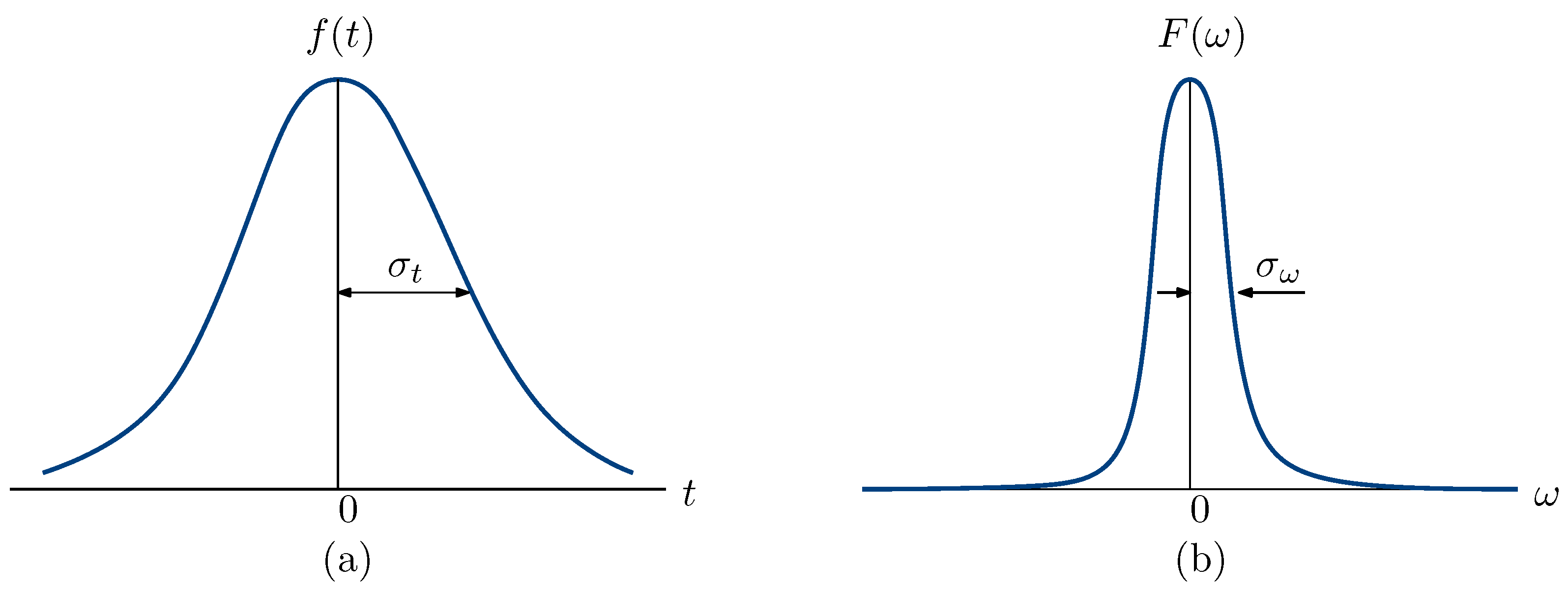
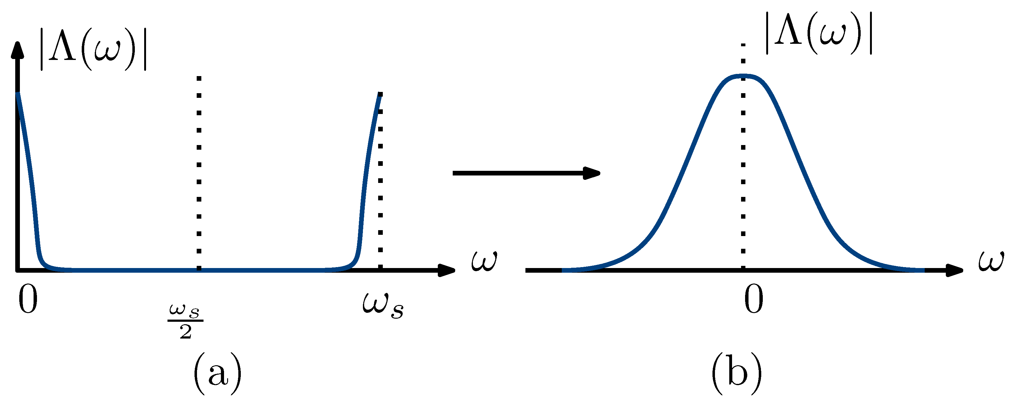
For a signal centered at zero, as illustrated in Figure 1, its time spread and frequency spread are defined in [22,23] as
where , , is the Fourier transform of and .
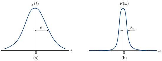
Figure 1.
(a) Time spread and (b) frequency spread of .
2.2. Heisenberg–Gabor Inequality
The time–frequency co-spread of is always higher than or equal to a given bound, which was introduced in [23,24] by the Heisenberg–Gabor inequality
The lower limit, one-half, corresponds to the optimal trade-off between the time–frequency localizations of . This bound can only be reached when is equal to the Gaussian function [20]
where is the time’s standard deviation of . Notice that is related to , but it is not the same parameter as . It yields .
2.3. Model of a Switching Waveform
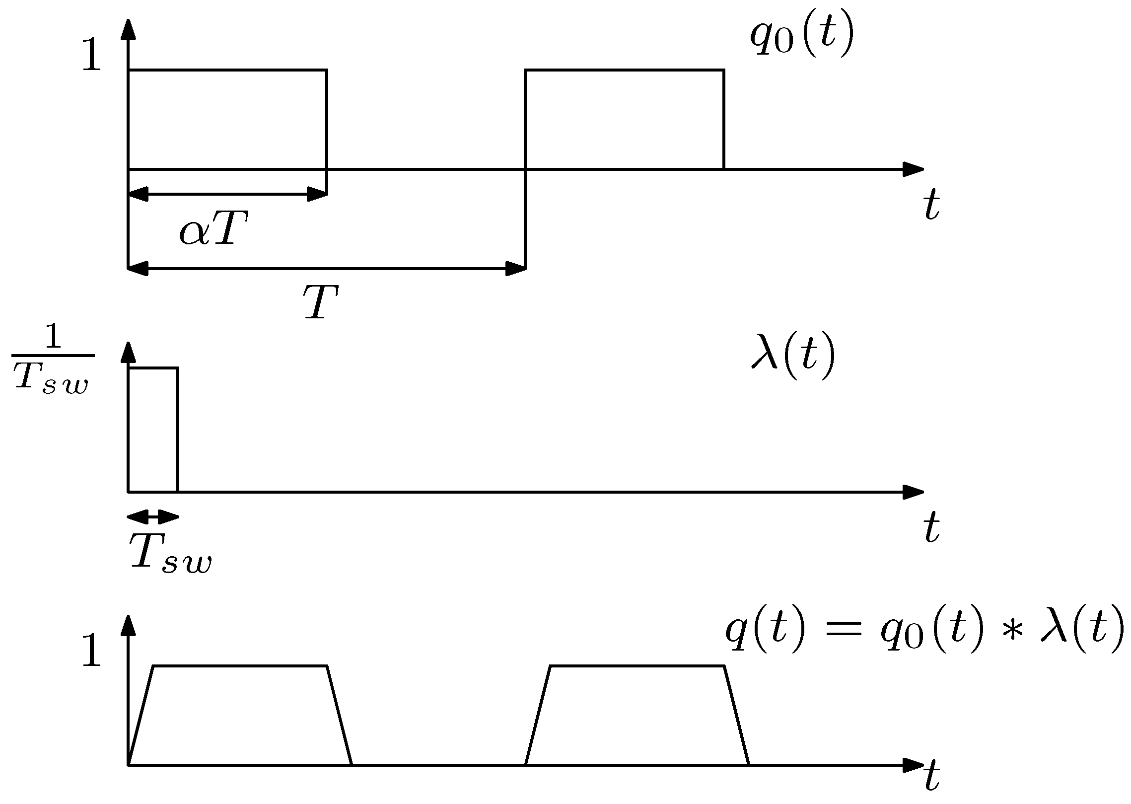
As described and explained in [4,20], a switching waveform of a power converter can be modeled as
where is an ideal square function whose edges are supposed as instantaneous and is a switching pattern. The resultant is a symmetric switching waveform whose rising and falling edges’ shape and duration are determined by . In the frequency domain, it corresponds to the product of the Fourier transform of and , denoted by and , respectively. For example, consider the symmetric trapezoidal waveform shown in Figure 2. This switching waveform is obtained by the convolution of the normalized square signal , with a period T and duty ratio , and the switching pattern over with . The duration of the rising and falling edges are the same and equal to .
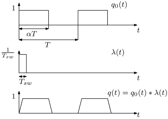
Figure 2.
Modeling of trapezoidal switching waveform by convolution.
2.4. Key Properties of Switching Patterns
The switching pattern is characterized by the time–frequency co-spread , which describes the trade-off between and . According to the Heisenberg–Gabor inequality, the smaller the switching time () is, the larger the spectral content () becomes. The optimal value is reached when the switching pattern is equal to the normalized Gaussian function (4). concentrates into a single number the relationship between the switching time (switching losses) and spectral content (EMI), which is an important issue in power electronics and is used to define the proposed FOM that will be introduced in the following section.
2.5. Figure of Merit Definition
In power electronics, the high levels of voltage and current switching edges ( and ) are sources of conducted and radiated EMI. They are propagated in a frequency range from 150 kHz to 30 MHz for conducted EMI and 30 MHz to 40 GHz for radiated emissions [25]. In order to reduce the EMI, a low magnitude value of the spectra is desired at frequencies where EMI are propagated. The spectrum frequency envelope of the switching waveforms is related to the edges’ duration and shape. The reduction can be reached either by increasing the switching duration, which implies increasing power losses, or by shaping the edges’ waveform. In this sense, different shapes of waveforms can have different spectra even when their switching durations are the same. Therefore, it is proposed to use the time–frequency co-spread to define a FOM that quantifies the EMI generation by the edges’ waveform. It concentrates the relationship between the switching duration and spectral content into a single number independently of the switching duration. Moreover, since obtains its optimal value with the Gaussian pattern (4), the proposed FOM allows for quantification of how close a switching waveform is to the optimal time and frequency trade-off.
2.5.1. Theoretical Analysis of Symmetric Waveforms
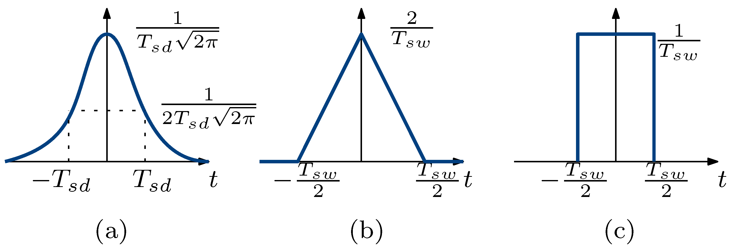
A switching waveform formed by the convolution of an ideal square function and a switching pattern is a symmetric waveform whose falling and rising edges have the same duration and shape. These falling and rising edges are determined by the switching pattern . Consider the three standard functions: the rectangular, the triangular, and the Gaussian functions (4), shown in Figure 3. These presented functions can be used as the switching pattern to form a switching waveform . The value of the co-spread of each switching pattern allows us to characterize the spectral content generated by the edges of the resultant and quantify how close is to the optimal case. In this sense, the time–frequency co-spread for each function is presented in Table 1. In the case of the rectangle, is indeterminate due to its extremely large spectral content. The values in Table 1 allow us to determine that a switching waveform formed with the triangular pattern has a time–frequency trade-off that is less optimal than that of the switching waveform formed with a Gaussian pattern. This implies that, for a switching waveform formed with the triangular pattern, increasing the switching duration reduces the spectral content in a smaller proportion than a Gaussian pattern.
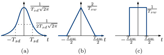
Figure 3.
(a) Gaussian function, (b) triangular function, and (c) rectangular function.

Table 1.
The time and frequency spreads of standard functions.
2.5.2. Practical Analysis for Non-Symmetric Waveforms
For a symmetric switching waveform , the switching pattern determines, in the same way, the duration and shape of both the falling and rising edges. Then, the parameter of the switching pattern allows us to quantify how close is to the optimal trade-off. However, in more realistic cases, the rising and falling edges of are not symmetric, and it is necessary to quantify the performance of each edge. To this end, one switching pattern can be associated with each edge, which can be denoted by for the rising and for the falling switching patterns. Then, it is possible to calculate for the rising and for the falling edges. It yields the following vector
Therefore, the FOM can be defined as
For the optimal symmetrical waveform, formed with the Gaussian switching pattern, the FOM value is
3. FOM Calculation
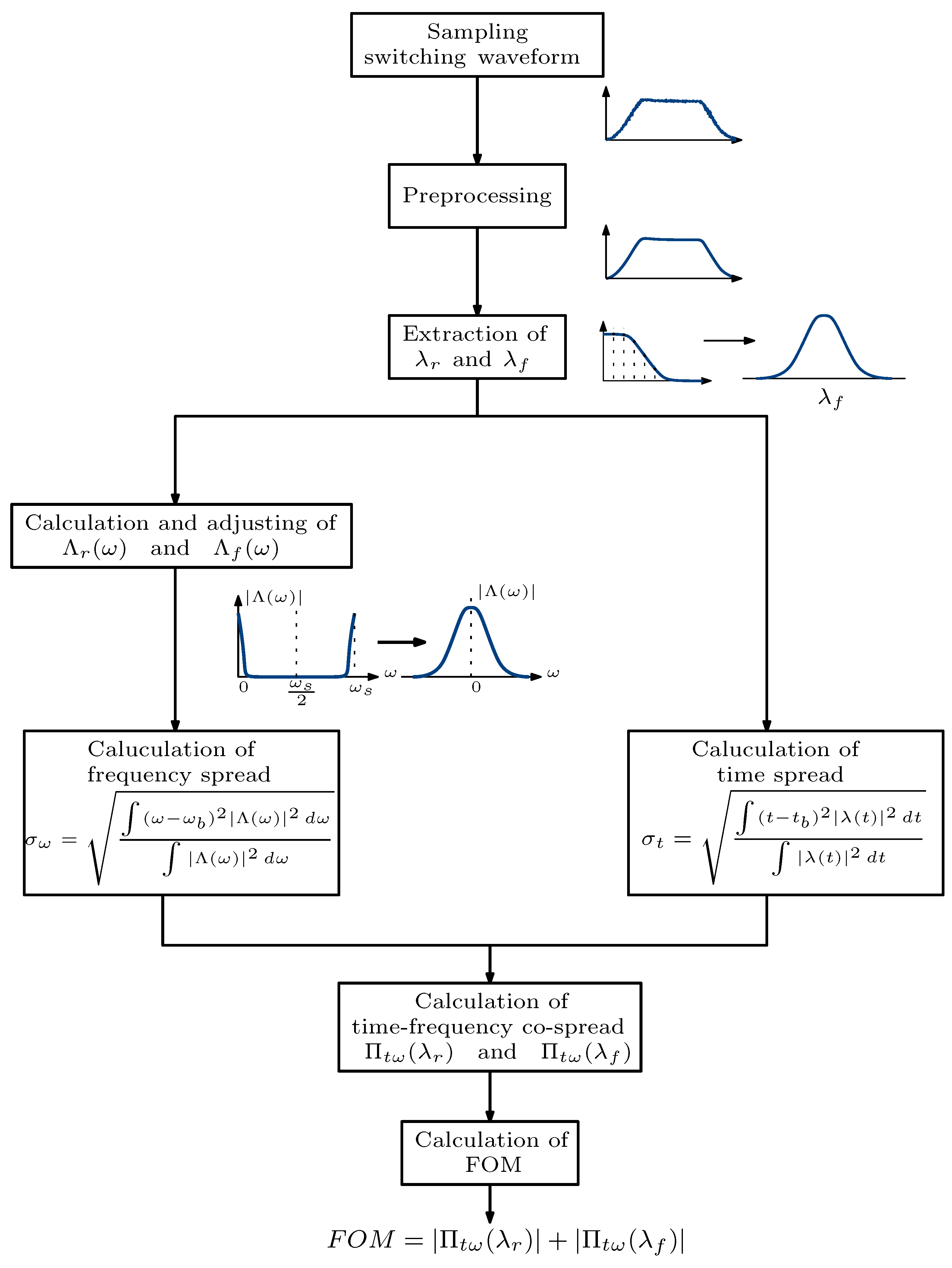
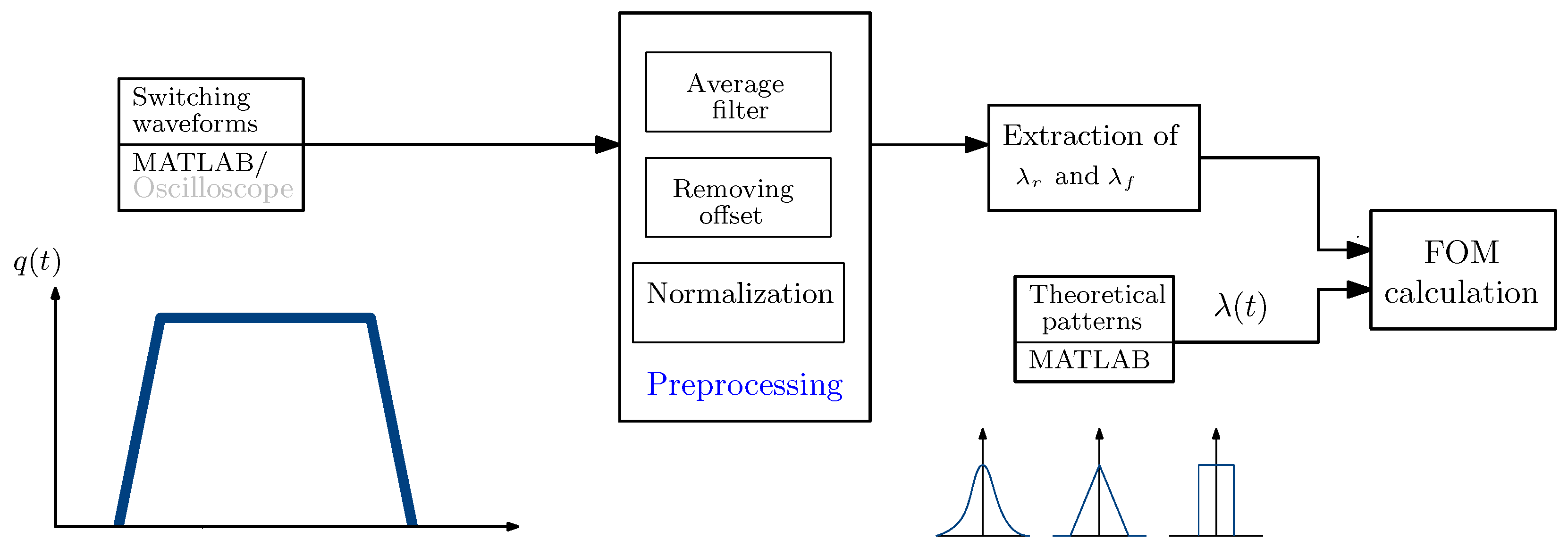
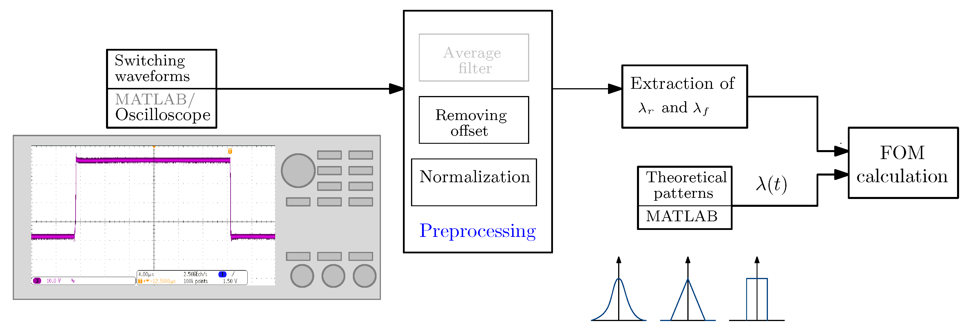
In order to characterize the switching waveforms from power electronic converters using the FOM, a calculation method is proposed in this section. This method is summarized in Figure 4, and it is focused on experimental switching waveforms. It allows us to calculate the FOM of fixed sampling period data, such as oscilloscope measures.
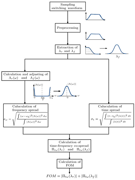
Figure 4.
FOM calculation method.
The calculation method is divided into the preprocessing stage, extraction of and , calculation of the time and frequency spread, calculation of the time–frequency co-spread, and calculation of the FOM. This method is detailed as follows.
3.1. Preprocessing
For the method proposed in this article, the first requirement to be fulfilled is that the evaluated switching waveform must be centered during measurement as shown in Figure 5.
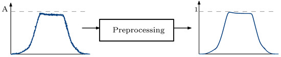
Figure 5.
Preprocessing of the switching waveforms for FOM calculation.
The vector of the samples of is defined as where k represents the kth sample. It is acquired with a fixed sampling period, and the number of samples (size) of is denoted by N. The preprocessing stage consists of averaging data, normalizing the sampled signal, and removing the offset. First, averaging is performed by using a moving average filter given by
where M is the number of samples in the average and the size of is also N. The size of the averaging is denoted by with . For this method, the use of is proposed to avoid modifying the shape of the switching edges. The averaged signal after this stage is shown in Figure 6, which keeps the shape of the rising and falling edges.
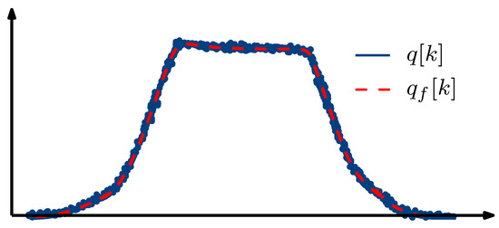
Figure 6.
Averaging switching waveform using a moving average filter.
In order to normalize and remove the offset, the vectors and are defined, respectively, considering the size of is N. The size of and can be expressed as a proportion of N as and . The vectors and are used to calculate the average amplitude and offset. For this method, = 0.1 and = 0.1 are proposed. Firstly, in order to detect the average offset of , the first sample of is . Since is centered, the offset vector contains the values when the switching waveform is supposed as equal to zero. For the normalization, the maximum average amplitude of is calculated. The sample is , which captures a vector of the maximum values since is centered. Then, computing the average of as
allows us to estimate the maximum amplitude of the switching waveform. In a similar way, the offset of is estimated by computing the average of as
and, consequently, the processed vector is expressed by
3.2. Extraction
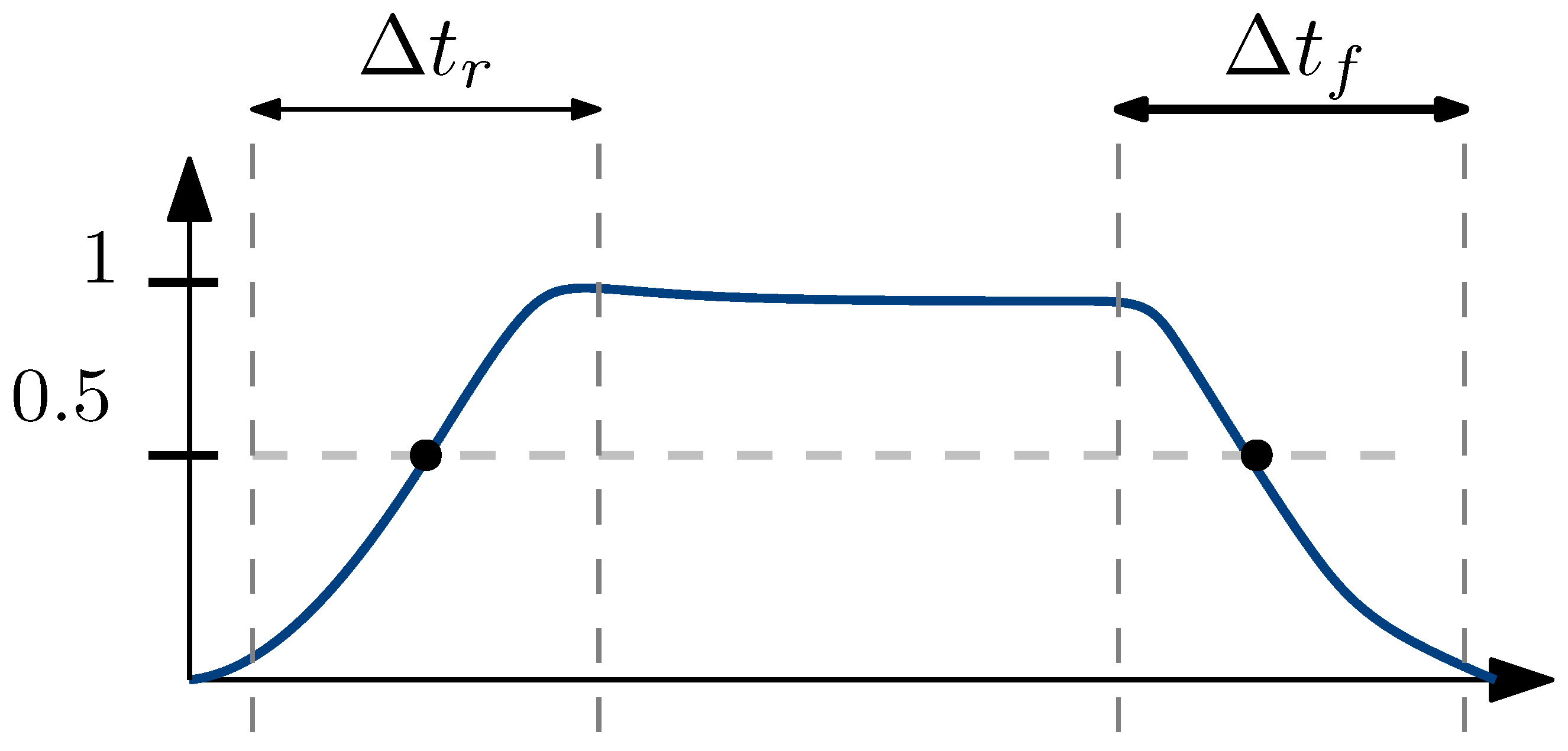
In order to extract the rising and falling switching patterns, the vectors and are defined. These vectors contain the rising and falling edges of the switching signal, respectively. Note that these vectors have an associated time vector and , respectively, which have the same size and indicate the time duration of each edge. To properly extract each edge, the sample in which the signal crosses the 0.5 value is identified. This event can occur at least twice, once during the rise and once during the fall. Considering that the size of and are and , and assuming that the sample in which the crossing with 0.5 for the rising edge is and for the falling edge is , then
with with = 0.01 and with = 0.01. This means the size of the rising and falling edges are 1% of the size. As shown in Figure 7, this allows us to extract a vector that contains both the rising and falling edges centered in the crossing 0.5 value. Then, the switching patterns are calculated with

Figure 7.
Extraction of switching patterns.
3.3. Calculation of and
For the calculation of the time spread , the first step is to calculate , which allows us to calculate using (1). Then, to calculate the frequency spread , calculate the discrete Fourier transform and obtain its amplitude spectrum, as shown in Figure 8a where is the sampling frequency such that and .

Figure 8.
(a) Amplitude spectrum of and (b) amplitude spectrum of centered at .
Notice that, for this step, it is necessary to have a fixed sampling period. The spectrum in Figure 8a is symmetric with respect to . Data from to can be used to recreate the negative part of the spectrum as a mirror copy to obtain a diagram centered to zero, as shown in Figure 8b. Since is centered at , , calculate using (2).
3.4. Time–Frequency Co-Spread and FOM Calculation
Computing the time–frequency co-spread of the rising and falling edges by
Finally, compute the FOM as follows
4. FOM Validation
In order to validate the FOM and the method proposed, they are implemented using MATLAB R2022b and compared with theoretical values. First, the FOM is calculated for two different switching patterns, the triangular and Gaussian patterns, as shown in the bottom of Figure 9, to validate the theoretical values. Then, the FOM is calculated using the method proposed in previous section for switching waveforms generated by convolution using MATLAB R2022b and taking as the switching patterns the triangular and Gaussian functions. Then, the results are compared with the theoretical values. Notice that this switching pattern can be replaced by the oscilloscope measures for an experimental application. Additionally, a comparison of the FOM calculation with the theoretical values at different sampling periods is performed in order to establish an adequate relation for the time spread and sampling period. Finally, the impact of Gaussian noise in the FOM calculation is evaluated.
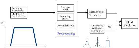
Figure 9.
Validation of FOM method.
4.1. Switching Pattern Evaluation
In order to validate the FOM calculation, calculation of the FOM for standard signals is proposed as a first test. Since, in this test, there is no extraction, only the calculation of time and frequency spread are validated. The standard triangular and Gaussian functions are selected, and they are generated in MATLAB R2022b with = 200 ns for the Gaussian function and = 500 ns for the triangular function. Then, the FOM is computed using (1) and (2). The results obtained are shown in Table 2 in the Theoretical column. The second test consists of calculating the FOM for switching waveforms formed with the standard functions as switching patterns. The switching waveforms are formed by the convolution of the switching pattern (triangular/Gaussian) and a square signal in MATLAB R2022b, and the following parameters are considered: the switching period is T = 50 s; for the Gaussian function, = 200 ns; for the triangular function, = 500 ns; and, for the sampling period, = 25 ns. Since the rising and falling edges are considered equal, only the FOM for one edge is calculated. The results in Table 2 show that the estimation of the FOM for the Gaussian and the triangular waveforms are close to the theoretical values, which means that an adequate extraction of the switching pattern has been carried out.
Table 2.
Values calculated using standard patterns.
4.2. Sampling Period
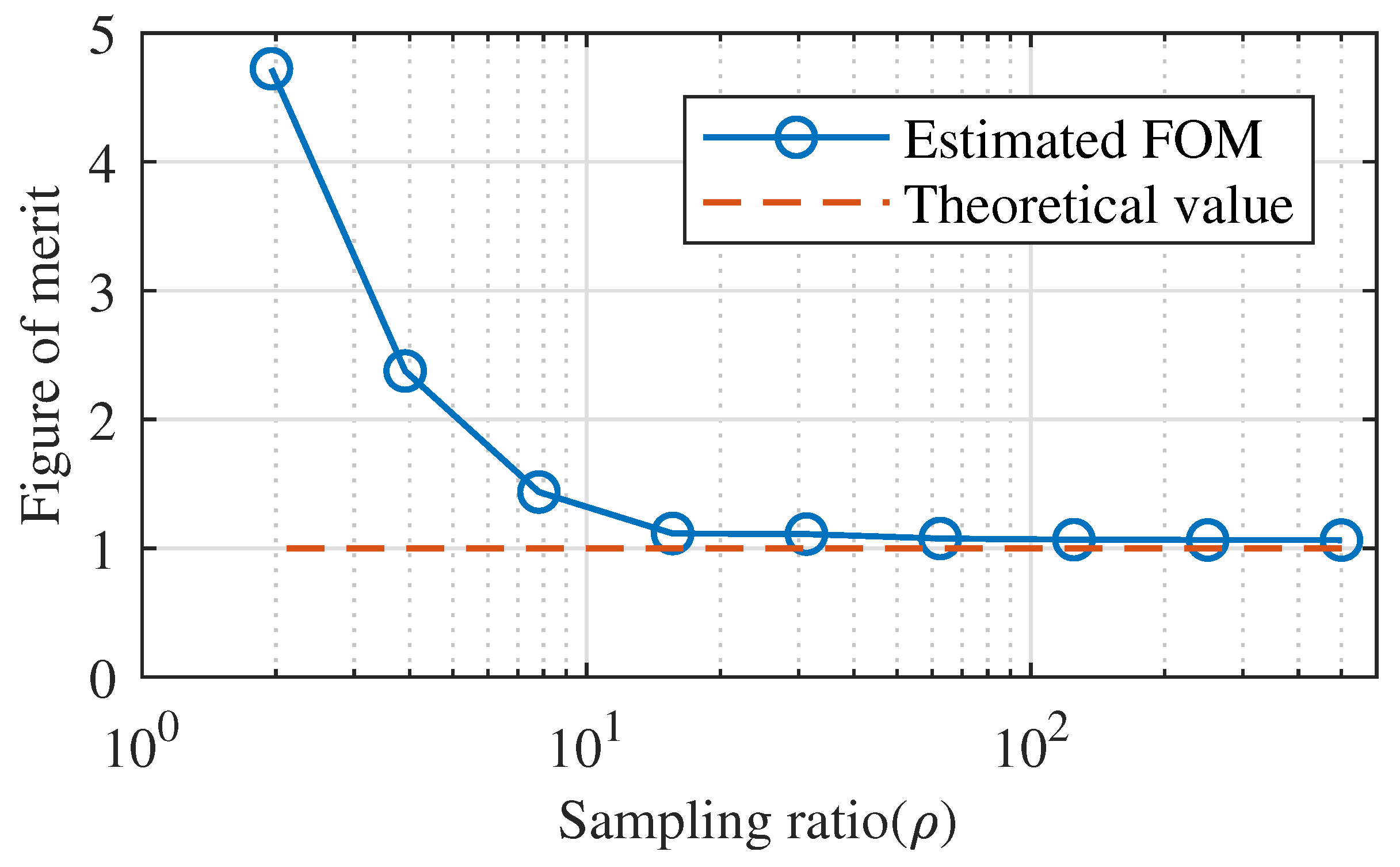
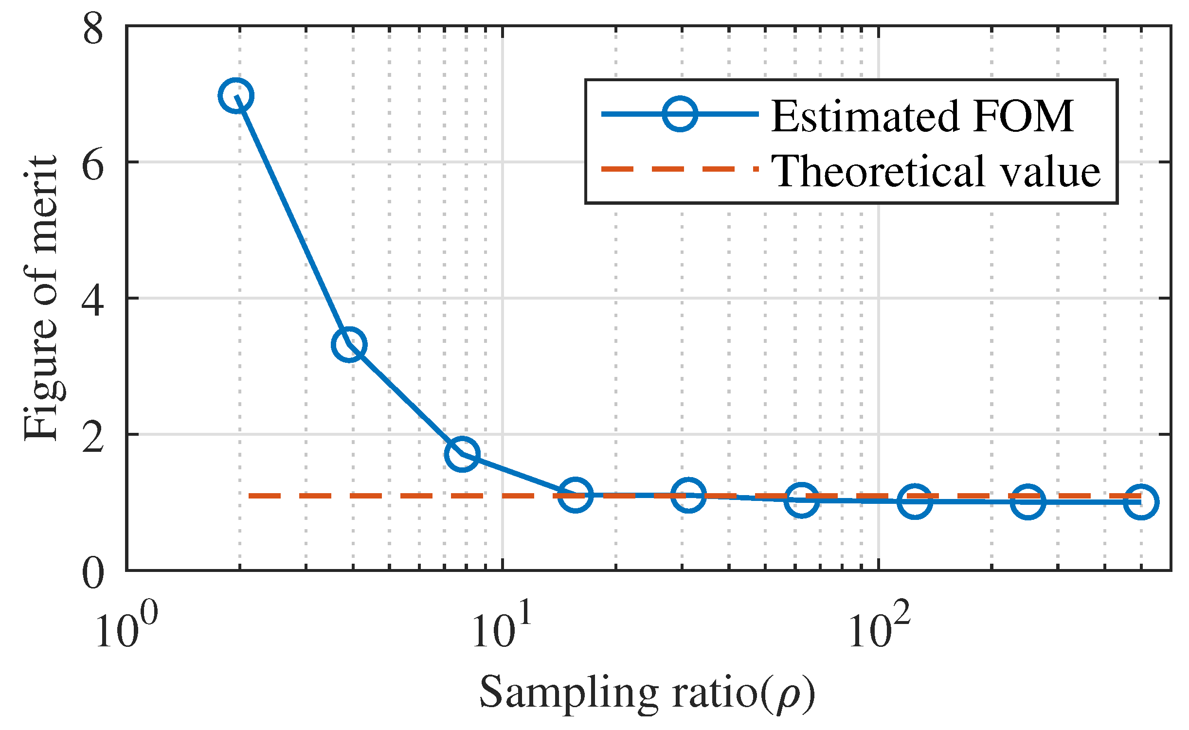
Since the proposed procedure to calculate the FOM depends on the sampling of the switching waveform edges, it is necessary to ensure an adequate sampling period in order to have reliable results. In this sense, consider the ratio
describes the relationship between the switching time’s duration () and the sampling period . This ratio is evaluated for the switching waveform , obtained with the Gaussian pattern, whose FOM value is one, and = 200 ns and for the triangular pattern with = 500 ns at several sampling periods. The test consists of varying the sampling period and comparing the FOM values obtained with the theoretical values. The results are presented in Figure 10 for the Gaussian pattern and in Figure 11 for the triangular pattern. From the results, it can be inferred that that > 10 is enough to estimate an adequate value of the FOM.
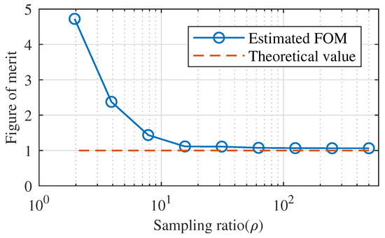
Figure 10.
Sampling ratio for the Gaussian-pattern FOM estimation.
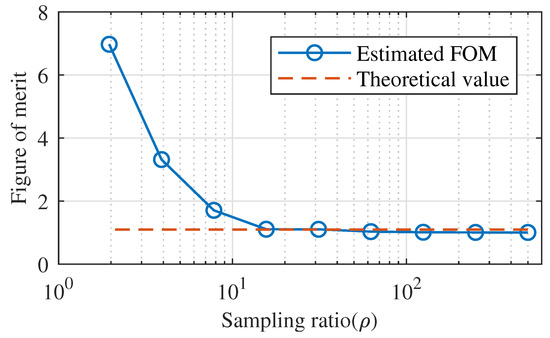
Figure 11.
Sampling ratio for the triangular-pattern FOM estimation.
4.3. Signal-to-Noise Ratio Evaluation
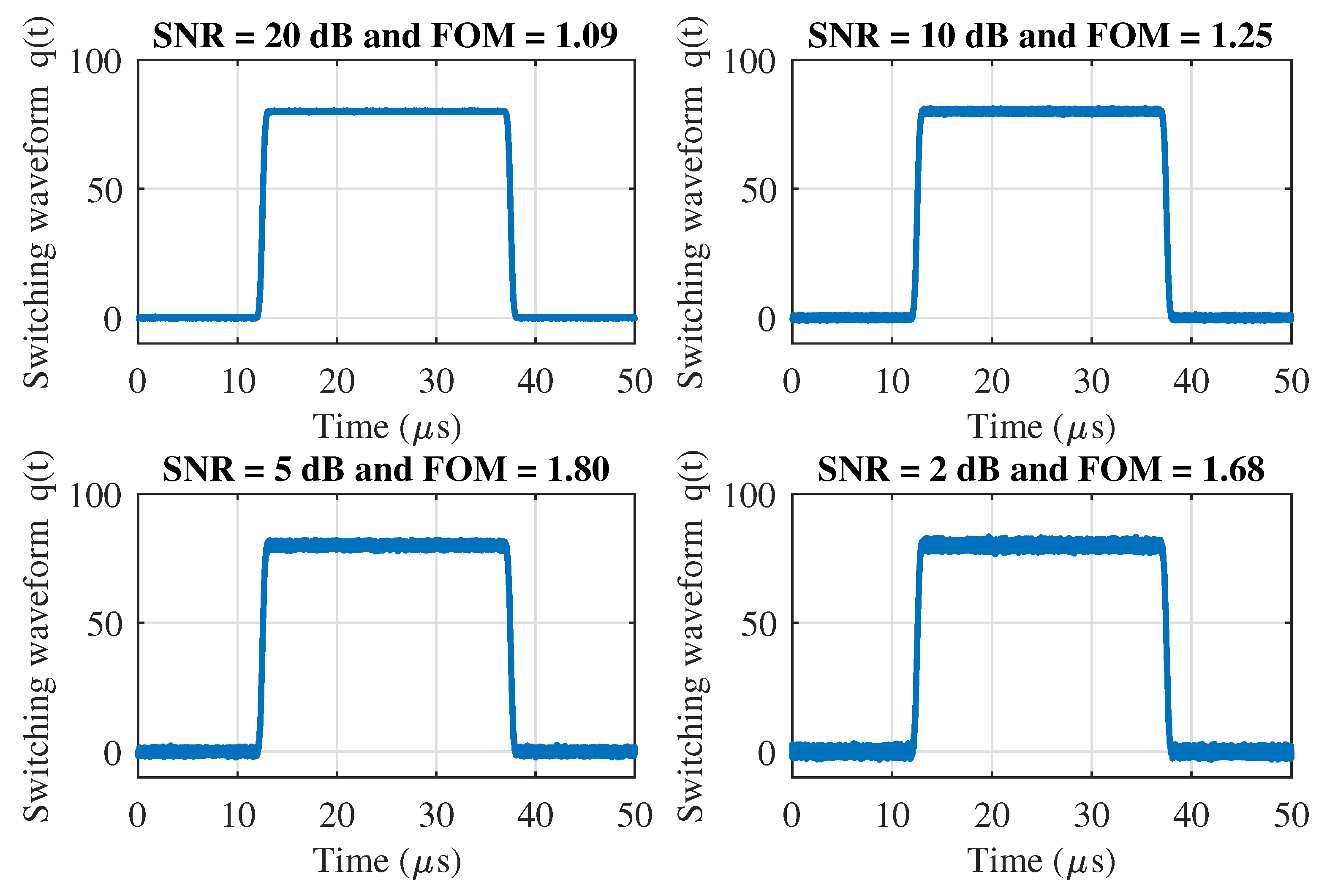
The presence of noise in the switching waveforms can affect the result of the FOM calculation. Therefore, a test at different noise levels is performed. The test consists of a form of a switching waveform, whose value is known, such that it is formed with the Gaussian pattern, and Gaussian noise is added. Then, the FOM is calculated, and the values obtained are compared with the theoretical value to observe the robustness of the proposed method. This test is made considering = 500 to ensure a reliable calculation. The results obtained are shown in Figure 12 for different levels of noise.
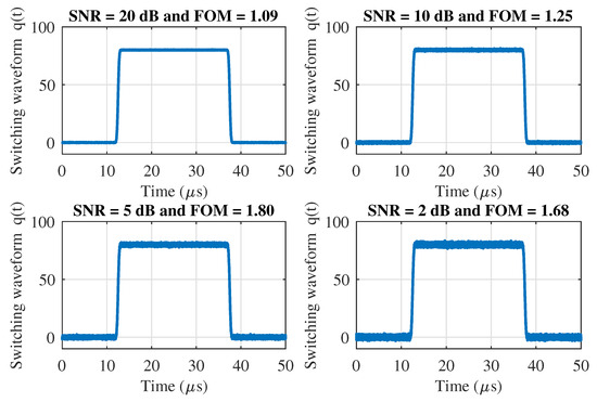
Figure 12.
Evaluation of the FOM calculation at different levels of noise.
As shown in Figure 12, the presence of noise in the switching pattern can affect the FOM calculation, which is a weakness of this methodology. A signal-to-noise ratio of 20 dB can modify FOM = 1 (expected) to FOM = 1.09 (triangular value). Therefore, the preprocessing stage is quite relevant in the calculation. Other alternatives can be explored in experimental applications, such as performing average filtering directly on an oscilloscope.
5. Practical Evaluation
The simplest way to reduce the EMI generated by the switching of insulated-gate power transistors consists of slowing down the switching duration by increasing the gate resistance. The proposed FOM is used to evaluate the impact of an increasing gate resistor value on EMI reduction in a experimental setup. This evaluation is summarized in Figure 13 and consists of driving an IGBT, using the circuit 1R2110, with different values of gate resistance. The voltage switching waveforms for each gate resistance are measured using an oscilloscope and evaluated with the proposed FOM.
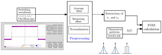
Figure 13.
Practical evaluation of the FOM.
5.1. Test Circuit
The evaluation is performed with the test circuit shown Figure 14 and the parameters presented in Table 3. The IGBT chosen is the IKW40N65ET7 [26]. The driver circuit selected is the IR2110 device, which is a standard circuit used in several power electronics applications. The gate resistance values chosen are
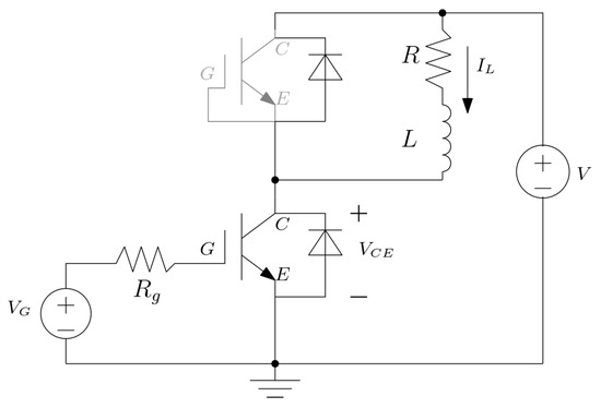
Figure 14.
Test circuit.
Table 3.
Simulation parameters.
The same resistance value is used both for turn-on and turn-off (in practice, this choice is not optimal). An oscilloscope Tektroniks model MS03054 is used to acquire the switching waveform with a sampling period of 400 ps.
5.2. Results
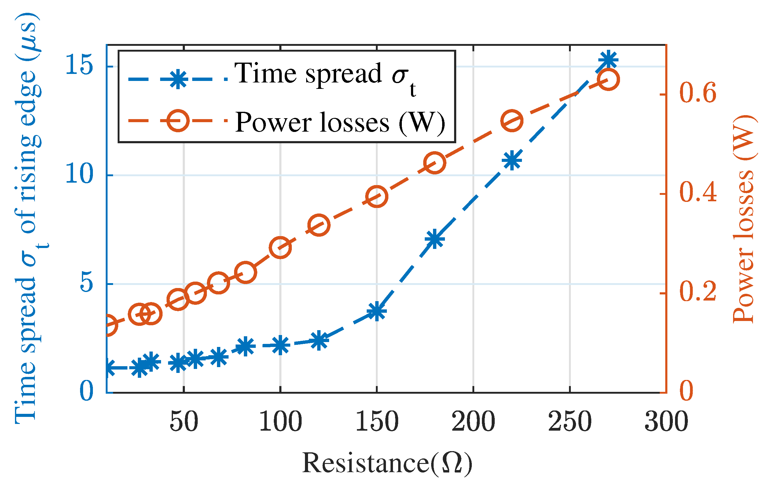
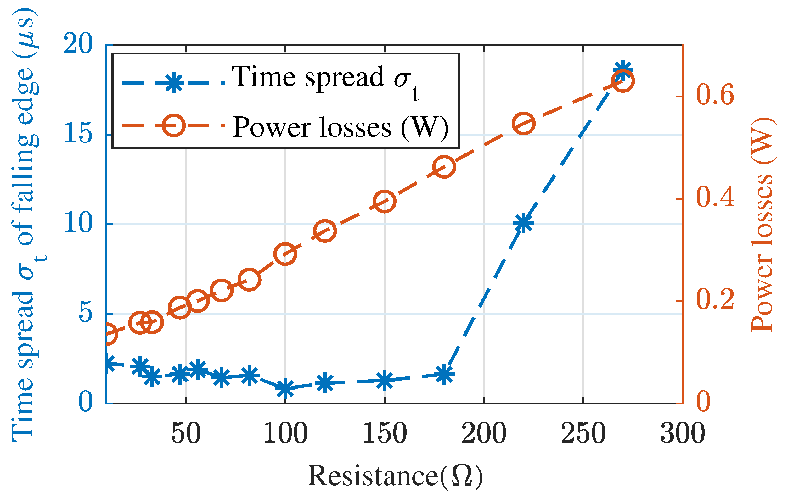
The time spread values () for the rising and falling edges measured at different gate resistances are shown in Figure 15 and Figure 16. As expected, increasing increases the switching duration, and, at the same time, it also increases the time spread but not in the same proportion. Additionally, the increase in switching power losses is presented in Figure 15 and Figure 16.
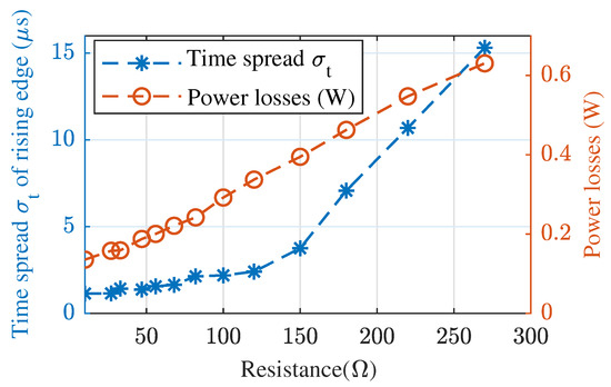
Figure 15.
Switching power losses and rising time spread for different gate resistance values.
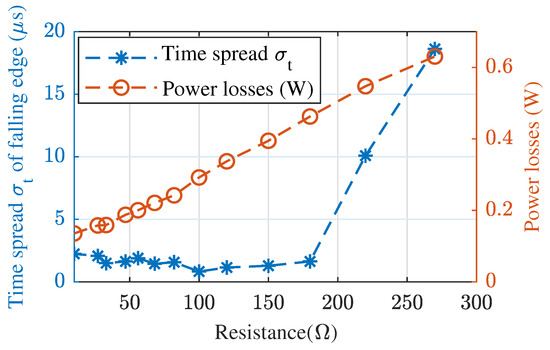
Figure 16.
Switching power losses and falling time spread for different gate resistance values.
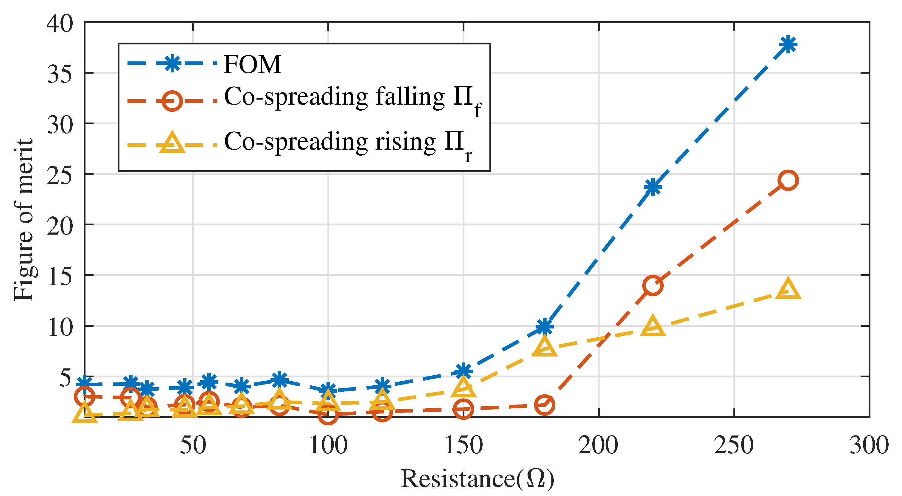
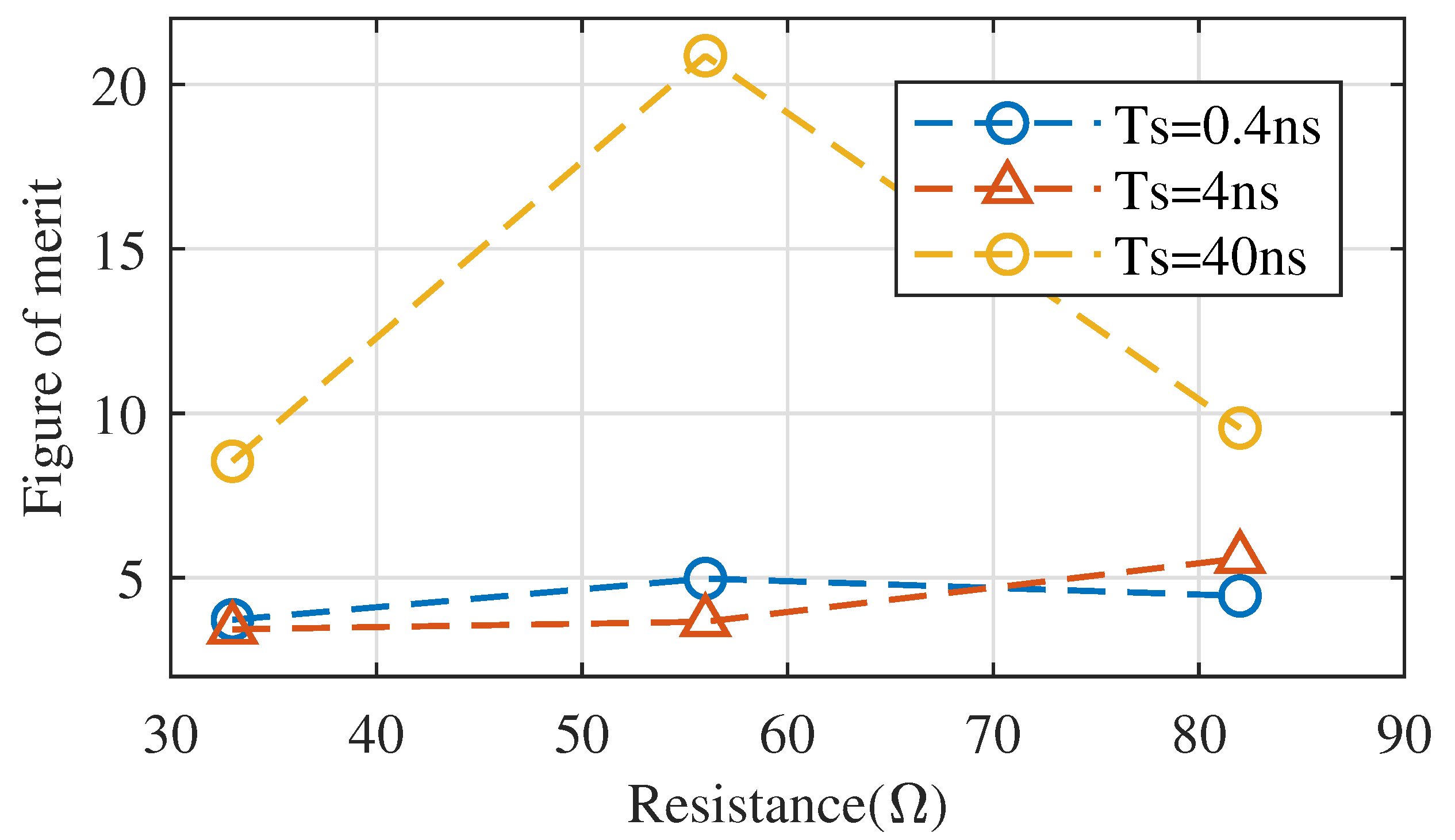
The results for the FOM calculation are presented in Figure 17. Notice that the FOM value is cloesr to the optimal value when < 150 than in the case when > 150 . By increasing the resistance more than 150 , the switching waveform tends to move away from the optimal value. Then, for > 150 , it is possible to infer that, despite increasing the switching time (), the spectral content () is not reduced in the same proportion as in < 150 . Additional information can be obtained with the time–frequency co-spread of the rising and falling edges. The falling edge is the one that tends to move further away from the optimal value. This information can be useful to improve the driving method. For example, it is possible to propose values of that improve the push–pull configuration, which uses two different resistance values for falling and rising.
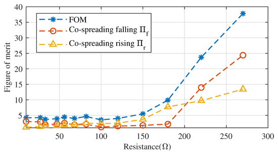
Figure 17.
FOM values at different values of .
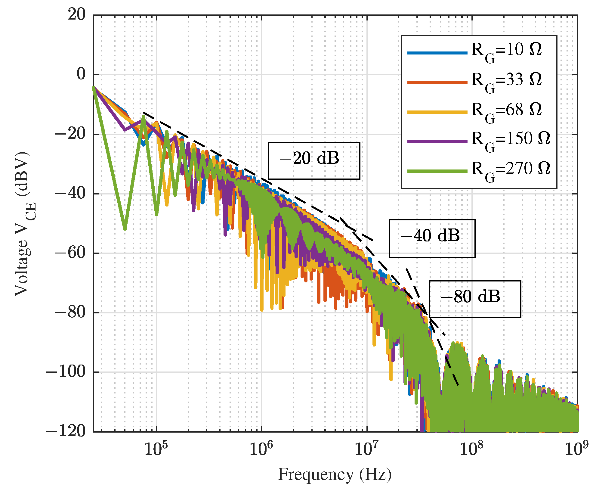
In order to determine the EMI generation for each switching waveform, the attenuation level of its voltage frequency spectrum is considered. Increasing the value of increases the switching duration and modifies the cut-off frequency of the frequency spectrum. In Figure 18, the voltage frequency spectra at different values of are presented. The different attenuation levels for each case can be observed. Furthermore, the way in which the cut-off frequency of each spectrum asymptote changes when the resistance increases can also be observed.

Figure 18.
Frequency spectra at different values.
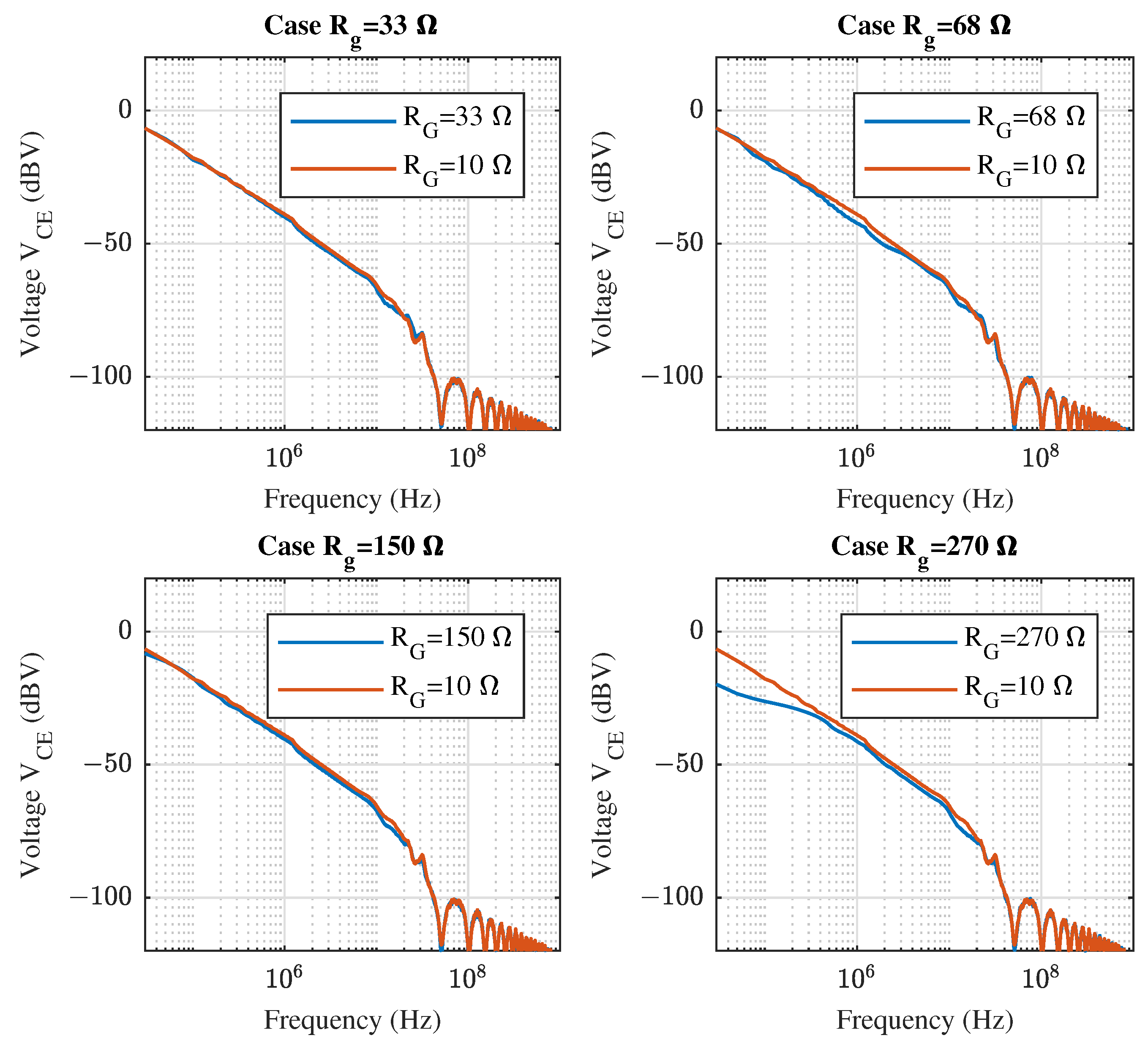
In addition, to complement these observations, an individual comparison of each average spectrum is presented. The average spectra for different values of are presented in Figure 19. The shortest switching duration corresponds to the case when = 10 and, therefore, corresponds to the largest generation of EMI. For this reason, the spectrum obtained with = 10 is compared with different values of in order to observe the EMI reduction when increases. From Figure 19, it is possible to observe that the EMI reduction is more significant when = 270 . It allows us to see the impact of increasing in the cut-off frequency and how the attenuation is increasing at some frequency bands.
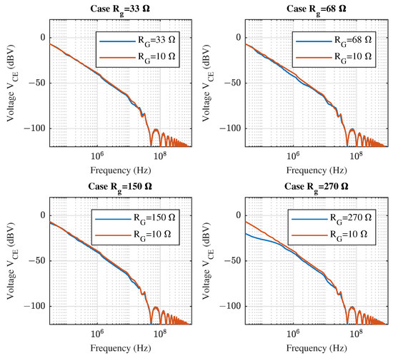
Figure 19.
Average frequency spectra at different values.
5.3. Sampling Period and Filtering
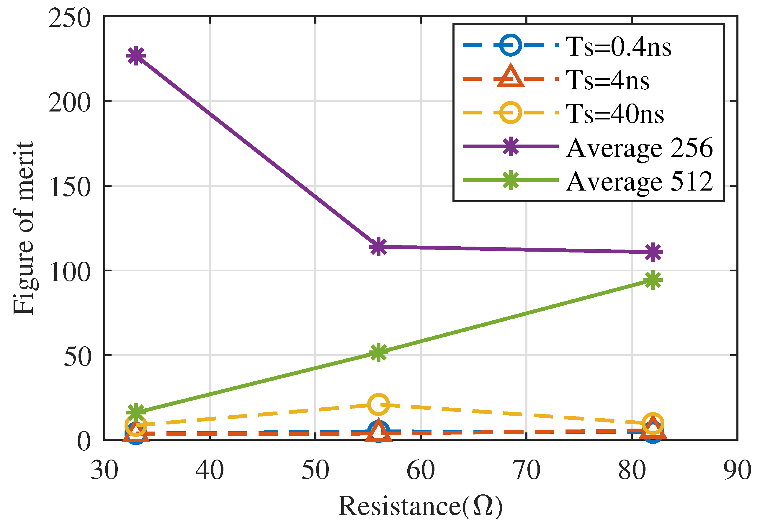
Additionally, the FOM calculation is evaluated in two different cases: at different sampling periods and replacing the algorithm average filtering with the averaging of the oscilloscope. In the first case, three different values of were selected, and the switching waveform acquisition was made using three different sampling periods. The FOM values obtained are presented in Figure 20. The FOM values tend to drift away when the sampling period increases, which can indicate that the ratio value does not satisfy the confidence criterion.
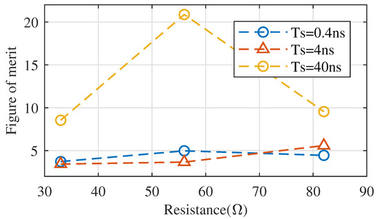
Figure 20.
FOM values at different sampling periods.
For the second test, which is summarized in Figure 21, the results obtained are presented in Figure 22. The FOM values move away from values obtained at different sampling periods, which shows the importance of the average filtering stage of the FOM algorithm. Using the average of the oscilloscope is not enough to keep in the confidence zone.
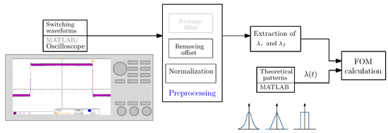
Figure 21.
FOM calculation without filtering stage.
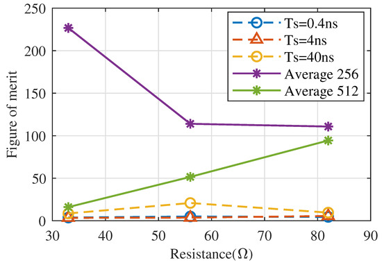
Figure 22.
FOM values using oscilloscope average filter.
6. Conclusions
This paper presents a method for calculating a FOM to evaluate the EMI generation of experimental switching waveforms from measurements of instruments such as an oscilloscope. Calculation of the FOM requires the extraction of the switching pattern of switching waveforms; these patterns are obtained by deriving the rising and falling edges. For this reason, the method proposed considers the duration of extraction, centering the extraction time interval and the sampling period. The method validation shows that the sampling period can affect the FOM. However, a criterion was established to ensure an adequate FOM calculation. Moreover, since switching patterns are obtained by deriving the rising and falling edges, the noise can compromise proper FOM calculation for the sampling method. In this sense, a preprocesing stage was proposed to average the data measurements and improve the FOM calculation. The FOM was used to evaluate the impact of increasing the gate resistance in an IGBT on the EMI generation. Increasing gate resistance implies increasing the switching time. The results show that, for , the FOM value is close to its optimum, but, for the FOM value moves away from its optimum as the gate resistance increases. This means that for , despite increasing the switching duration (), the spectral content is not reduced in the same proportion as . Therefore, for , the switching waveform generates proportionally less EMI and fewer switching power losses than . This FOM implementation allows us to optimize the value selection. Additionally, FOM calculation is affected by choosing an inadequate sampling period or filtering stage, which is a limitation of this method; however, the FOM is easily implementable with a suitable oscilloscope and a processing software such as MATLAB R2022b. This FOM can be used not only to optimize parameter values such as but also to compare different driver methodologies. Since the FOM shows a time–frequency relationship independent of the switching duration, it is less complex to define a comparative benchmark between two different driving methods.
Author Contributions
Conceptualization and development, D.S.M.-P., N.P., and E.M.; analysis and investigation, D.S.M.-P., N.P., and E.M. All authors have read and agreed to the published version of the manuscript.
Funding
This work was funded by the Consejo Nacional de Humanidades, Ciencias y Tecnologías (CONAHCyT) under grant agreement: 705759.
Data Availability Statement
The data presented in this study are available on request from the corresponding author.
Conflicts of Interest
The authors declare no conflict of interest.
References
- Zhang, R.; Chen, W.; Zhou, Y.; Shi, Z.; Yan, R.; Yang, X. Mathematical Modeling of EMI Spectrum Envelope Based on Switching Transient Behavior. IEEE J. Emerg. Sel. Top. Power Electron. 2022, 10, 2497–2515. [Google Scholar] [CrossRef]
- Bi, C.; Lu, R.; Li, H. Prediction of Electromagnetic Interference Noise in SiC MOSFET Module. IEEE Trans. Circuits Syst. II Express Briefs 2019, 66, 853–857. [Google Scholar] [CrossRef]
- Meng, J.; Ma, W.; Pan, Q.; Zhang, L.; Zhao, Z. Multiple Slope Switching Waveform Approximation to Improve Conducted EMI Spectral Analysis of Power Converters. IEEE Trans. Electromagn. Compat. 2006, 48, 742–751. [Google Scholar] [CrossRef]
- Costa, F.; Magnon, D. Graphical analysis of the spectra of EMI sources in power electronics. IEEE Trans. Power Electron. 2005, 20, 1491–1498. [Google Scholar] [CrossRef]
- Oswald, N.; Stark, B.H.; Holliday, D.; Hargis, C.; Drury, B. Analysis of Shaped Pulse Transitions in Power Electronic Switching Waveforms for Reduced EMI Generation. IEEE Trans. Ind. Appl. 2011, 47, 2154–2165. [Google Scholar] [CrossRef]
- Consoli, A.; Musumeci, S.; Oriti, G.; Testa, A. An innovative EMI reduction design technique in power converters. IEEE Trans. Electromagn. Compat. 1996, 38, 567–575. [Google Scholar] [CrossRef]
- Musumeci, S.; Raciti, A.; Testa, A.; Galluzzo, A.; Melito, M. Switching-behavior improvement of insulated gate-controlled devices. IEEE Trans. Power Electron. 1997, 12, 645–653. [Google Scholar] [CrossRef]
- Chen, L.; Peng, F.Z. Closed-Loop Gate Drive for High Power IGBTs. In Proceedings of the 2009 Twenty-Fourth Annual IEEE Applied Power Electronics Conference and Exposition, Washington, DC, USA, 15–19 February 2009; pp. 1331–1337. [Google Scholar]
- Lobsiger, Y.; Kolar, J.W. Closed-Loop di/dt and dv/dt IGBT Gate Driver. IEEE Trans. Power Electron. 2015, 30, 3402–3417. [Google Scholar] [CrossRef]
- Riazmontazer, H.; Rahnamaee, A.; Mojab, A.; Mehrnami, S.; Mazumder, S.K.; Zefran, M. Closed-loop control of switching transition of SiC MOSFETs. In Proceedings of the 2015 IEEE Applied Power Electronics Conference and Exposition (APEC), Charlotte, NC, USA, 15–19 March 2015; pp. 782–788. [Google Scholar]
- Wang, Z.; Shi, X.; Tolbert, L.M.; Wang, F.; Blalock, B.J. A di/dt Feedback-Based Active Gate Driver for Smart Switching and Fast Overcurrent Protection of IGBT Modules. IEEE Trans. Power Electron. 2014, 29, 3720–3732. [Google Scholar] [CrossRef]
- Idir, N.; Bausiere, R.; Franchaud, J.J. Active gate voltage control of turn-on di/dt and turn-off dv/dt in insulated gate transistors. IEEE Trans. Power Electron. 2006, 21, 849–855. [Google Scholar] [CrossRef]
- Huang, X.; Wang, F.; Liu, Y.; Lin, F.; Sun, H.; Yang, Z. Multi-Level Synthesis Gate Voltage Active Control Technology for Optimizing IGBT Switching Characteristics. IEEE J. Emerg. Sel. Top. Power Electron. 2023, 11, 2918–2929. [Google Scholar] [CrossRef]
- Takayama, H.; Okuda, T.; Hikihara, T. A Study on Suppressing Surge Voltage of SiC MOSFET Using Digital Active Gate Driver. In Proceedings of the 2020 IEEE Workshop on Wide Bandgap Power Devices and Applications in Asia (WiPDA Asia), Suita, Japan, 23–25 September 2020; pp. 1–5. [Google Scholar]
- Morikawa, R.; Sai, T.; Hata, K.; Takamiya, M. New Gate Driving Technique Using Digital Gate Driver IC to Reduce Both EMI in Specific Frequency Band and Switching Loss in IGBTs. In Proceedings of the 2020 IEEE 9th International Power Electronics and Motion Control Conference (IPEMC2020-ECCE Asia), Nanjing, China, 29 November–2 December 2020; pp. 644–651. [Google Scholar]
- Horii, K.; Yano, H.; Hata, K.; Wang, R.; Mikami, K.; Hatori, K.; Tanaka, K.; Saito, W.; Takamiya, M. Large-Current Output Digital Gate Driver for 6500 V, 1000 A IGBT Module to Reduce Switching Loss and Collector Current Overshoot. IEEE Trans. Power Electron. 2023, 38, 8075–8088. [Google Scholar] [CrossRef]
- Yang, X.; Yuan, Y.; Zhang, X.; Palmer, P.R. Shaping High-Power IGBT Switching Transitions by Active Voltage Control for Reduced EMI Generation. IEEE Trans. Ind. Appl. 2015, 51, 1669–1677. [Google Scholar] [CrossRef]
- Mohsenzade, S. A High-Voltage Series-Stacked IGBT Switch With Output Pulse Shaping Capability to Reduce EMI Generation. IEEE Trans. Electromagn. Compat. 2022, 64, 559–568. [Google Scholar] [CrossRef]
- Walder, S.; Yuan, X.; Laird, I.; Dalton, J.J.O. Identification of the temporal source of frequency domain characteristics of SiC MOSFET based power converter waveforms. In Proceedings of the 2016 IEEE Energy Conversion Congress and Exposition (ECCE), Milwaukee, WI, USA, 18–22 September 2016; pp. 1–8. [Google Scholar]
- Patin, N.; Viñals, M.L. Toward an optimal Heisenberg’s closed-loop gate drive for Power MOSFETs. In Proceedings of the IECON 2012—38th Annual Conference on IEEE Industrial Electronics Society, Montreal, QC, Canada, 25–28 October 2012; pp. 828–833. [Google Scholar]
- Martinez-Padron, D.S.; Patin, N.; Monmasson, E. Definition and Implementation of an EMI Figure of Merit for Switching Pattern in Power Converters. In Proceedings of the IECON 2022—48th Annual Conference of the IEEE Industrial Electronics Society, Brussels, Belgium, 17–20 October 2022; pp. 1–6. [Google Scholar]
- Akansu, A.N.; Haddad, R.A. Chapter 5—Time-Frequency Representations. In Multiresolution Signal Decomposition, 2nd ed.; Akansu, A.N., Haddad, R.A., Eds.; Academic Press: Cambridge, MA, USA, 2001; pp. 331–390. ISBN 9780120471416. [Google Scholar]
- Patin, N. 1—Introduction to EMC, Power Electronics Applied to Industrial Systems and Transports; Elsevier: Amsterdam, The Netherlands, 2015; Volume 4, pp. 1–21. [Google Scholar]
- Gabor, D. Theory of communication. Part 1: The analysis of information. J. Inst. Electr. Eng. Part III Radio Commun. Eng. 1946, 93, 429–441. [Google Scholar] [CrossRef]
- Paul, C.R. Introduction to Electromagnetic Compatibility, 2nd ed.; Wiley: Hoboken, NJ, USA, 2006. [Google Scholar]
- Infineon. Low Loss Duopack: IGBT with Trench and Fieldstop Technology IKW40N65ET7, TRENCHSTOP; Datasheet Version 2.2; Infineon Technologies: Neubiberg, Germany, 2020. [Google Scholar]


Disclaimer/Publisher’s Note: The statements, opinions and data contained in all publications are solely those of the individual author(s) and contributor(s) and not of MDPI and/or the editor(s). MDPI and/or the editor(s) disclaim responsibility for any injury to people or property resulting from any ideas, methods, instructions or products referred to in the content. |
© 2024 by the authors. Licensee MDPI, Basel, Switzerland. This article is an open access article distributed under the terms and conditions of the Creative Commons Attribution (CC BY) license (https://creativecommons.org/licenses/by/4.0/).