Abstract
DC distribution systems have garnered interest in recent years due to their advantages over AC distribution systems, such as their high power conversion efficiency and lack of harmonic issues. An isolated DC-DC converter with low-input noise, high efficiency, and high-power density is required for DC microgrids within DC distribution systems. Although existing DC to DC converters have high efficiency and high power density, they still have input noise problems due to pulsating input currents. Thus, a large input filter should be inserted, which increases the cost and degrades the power density. In this study, a novel three-level double LLC resonant converter with zero-input-current ripple is presented for DC microgrid application with a high-voltage DC bus. The input-current ripple of the proposed converter theoretically decreases to zero without adding large input filters. Moreover, the voltage stress on each main switch is only half of the input voltage when using the modified three-level structure, which enables the use of low-voltage-rated power switches for high-voltage input applications. In addition, all the primary switches and secondary diodes are softly switched over a wide input voltage range. The experimental results of the prototype are presented to verify the performance of the proposed converter.
1. Introduction
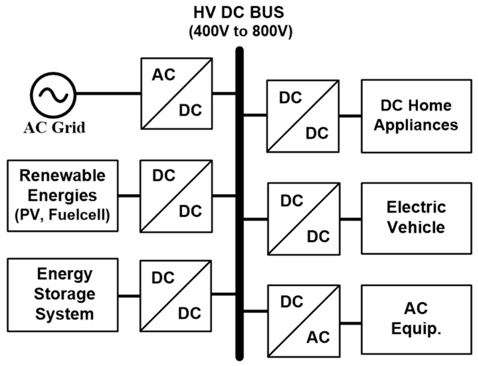
Recently, with the rapid growth of renewable energy systems and electric vehicles, research on DC distribution systems has been actively carried out due to their advantages over AC distribution systems, such as their high power conversion efficiency and lack of harmonic issues [1,2,3,4,5,6]. In addition, DC microgrids are considered to be the most viable solution for integrating renewable energy systems and energy storage systems, with DC loads such as electric vehicles and DC home appliances. Figure 1 shows a DC microgrid with DC distribution systems. To convert the high-voltage (HV) DC bus input to a low-voltage output for DC loads, an isolated DC-DC converter is required with the characteristics of low-input noise, high efficiency, and high power density. Half-bridge LLC resonant converters are popularly employed for DC loads in DC microgrids [7,8,9,10,11] because the main switches and rectifier diodes can be operated under zero-voltage switching (ZVS) and zero-current switching (ZCS) conditions over a wide input voltage range, respectively, which enables high efficiency to be achieved. For DC loads in DC microgrids with a higher DC bus voltage, three-level (TL) LLC resonant converters can be used. A fixed-frequency-controlled hybrid full-bridge (HFB) TL LLC resonant converter was introduced in [12]. All of the main switches were softly switched, and the voltage stress on each primary switch was half the input voltage. However, its efficiency was lower than that of variable-frequency-controlled LLC resonant converters. Another TL LLC resonant converter [13] was presented. Its output voltage regulation was achieved by pulse frequency modulation (PFM), which improved the efficiency of the TL LLC converter with fixed-frequency control [12]. However, to ensure that the voltage stress on each switch was maintained at half the input voltage, dead-time zones were additionally required in their driving signals, which made the driving circuits more complex. In [14], a TL double LLC (DLLC) resonant converter was proposed, which improved the complexity of the driving circuit. Moreover, it has constant high efficiency and a soft-switching ability over a wide input voltage range. However, in terms of the input-current ripple, all circuit topologies mentioned above are buck-derived topologies with a discontinuous input current, causing di/dt noise on the input side. Thus, a large input filter should be inserted, which increases the cost and degrades power density.
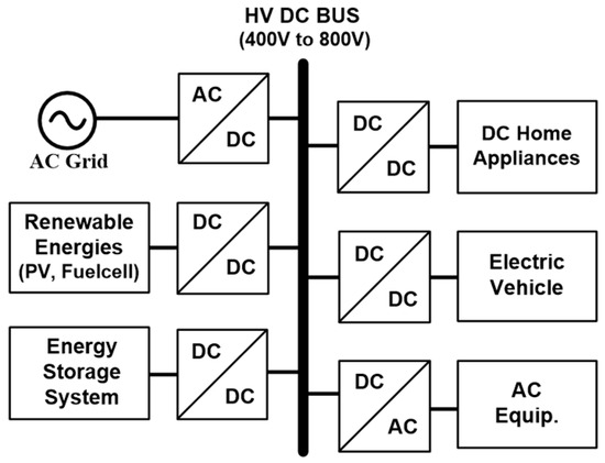
Figure 1.
Configuration of DC microgrid within DC distribution systems.
To minimize the input-current ripple, firstly, current-fed converters with a continuous input current [15,16,17,18] can be considered, but because most of them are boost topologies, they are not suitable for applications with high inputs and low outputs, unlike those with step-down buck-derived topologies. As another solution, a half-bridge converter with input-current-ripple reduction (HBC-CRR) [19] was presented. Although it is a buck-derived topology, its input-current ripple is reduced substantially by using two split windings and a clamp capacitor. However, its primary switches and secondary diodes operate under hard-switching conditions, and its secondary diodes have high-voltage stress during small-duty operation, increasing power losses. In [20], a novel high-efficiency LLC resonant converter was proposed, which improved the drawbacks of hard-switching operation and high-voltage stress on the secondary diodes in [19]. However, for higher-voltage input applications, all the primary switches suffer from high-voltage stress, resulting in high cost and poor efficiency.
In this paper, a novel high-efficiency TL double LLC resonant converter with zero input-current ripple and low-voltage stress is presented for high-voltage input applications. The input noise components, due to input current pulsation, are significantly reduced without the addition of bulky input filters. Moreover, the voltage across each primary switch is clamped to half the input voltage, which allows the use of low-voltage-rated power switches for high-voltage input applications. In addition, all primary switches and secondary diodes operate with ZVS turn-on and ZCS turn-off over a wide input voltage range, which enables high efficiency to be achieved.
2. Proposed TL Double LLC Resonant DC-DC Converter
2.1. Circuit Description
The circuit diagram of the proposed resonant converter is shown in Figure 2. It is a three-level double LLC resonant tank converter based on a structure that combines two LLC resonant converters in series with clamp capacitors. (S1, S3) and (S2, S4) are treated as two switch pairs. The gate signals for each switch pair, which are 180° out of phase, are driven at a constant duty cycle of 0.5, with pulse frequency modulation (PFM) control. Thus, in a series-interleaved double LLC resonant structure, the input-current ripple with a phase difference of 180° is canceled out and theoretically becomes zero regardless of the input voltage and load variations. Moreover, because it is a three-level topology with double LLC resonant tanks, the voltage across each primary switch is maintained at half the input voltage, and all primary switches and secondary diodes operate in ZVS turn-on and ZCS turn-off, respectively, over a wide input voltage range, reducing the switching loss. In addition, there are almost no voltage spikes across the primary switches after they are turned off, since the inductance energy of the resonant inductors and transformer magnetizing inductances is absorbed by the clamp capacitors. As a result, no snubber is required, and switching losses are improved.
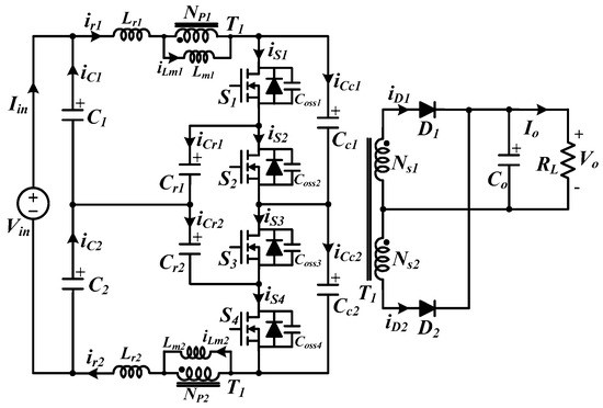
Figure 2.
Circuit diagram of proposed resonant converter.
To simplify the analysis, several assumptions are made:
- The output capacitor Co is large enough that the output voltage Vo and output current Io can be considered constant during a switching period Ts.
- The capacitances of the clamp capacitors Cc1 and Cc2 are sufficiently large; therefore, the voltage of the clamp capacitors can be assumed to be constant. They are equal to Cc.
- The input capacitors C1 and C2 are equal to C.
- The resonant capacitors Cr1 and Cr2 are equal to Cr.
- The resonant inductors Lr1 and Lr2 are equal to Lr.
- The parasitic output capacitances of the four primary switches are equal to Coss and treated as constant values during the dead-time period.
- The main transformer has windings: NP1 = NP2 = NP; a turn ratio: n = NP/NS; and a magnetizing inductance: Lm1 = Lm2 = Lm.
2.2. Operation Principle
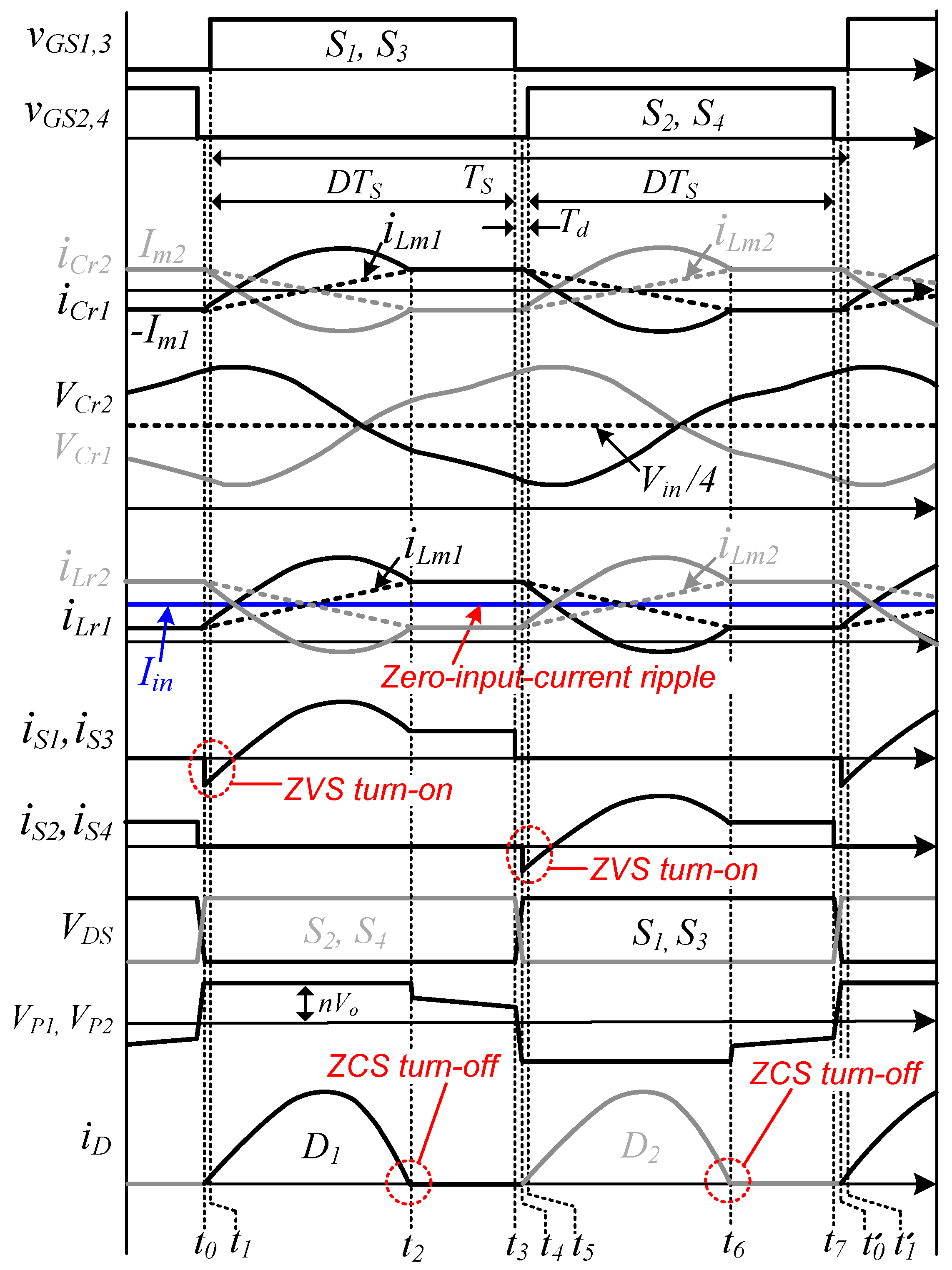
Figure 3 and Figure 4 show the key waveforms and operation modes of the proposed resonant converter, respectively. The resonant inductances (Lr1 and Lr2), transformer magnetizing inductances (Lm1 and Lm2), resonant capacitors (Cr1 and Cr2), and switch output capacitors (Coss) are assumed to be identical to each other. Since double LLC resonant tanks are connected in parallel, when one switch operates, the two LLC resonant tanks are involved in the operation at the same time. The clamp capacitors (Cc1 and Cc2) are charged with the same voltage, as Vin/2, and act as another voltage source. Prior to t0, all secondary diodes are in their off-state, and the output is separated from the primary side. Lr and Lm resonate with Cr, and iLr1 and iLr2 are equal to iLm1 = −Im1 and iLm2 = Im2, respectively, where Im1 and Im2 are the peak currents of the magnetizing inductance.
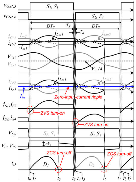
Figure 3.
Key waveforms of the proposed resonant converter.
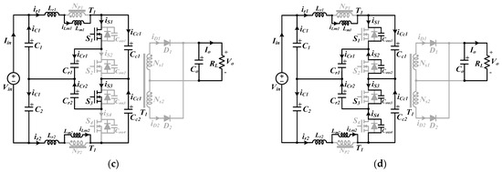
Figure 4.
Operation modes of the proposed converter in half cycle. (a) Mode 1, (b) Mode 2, (c) Mode 3, and (d) Mode 4.
(1) Mode 1 [t0, t1]: Mode 1 begins when the of S1/S3 and S2/S4 is completely discharged and charged, respectively, and the body diodes of S1 and S3 start to conduct at t0. D1 begins conducting. The primary voltages of the transformers VP1 and VP2 are clamped by the reflected voltage nVo. The iLm1(t) and iLm2(t) are linearly increased and decreased by nVo, respectively. A difference of half the input voltage Vin/2 and the reflected voltage nVo is applied to each resonant tank, and Lr and Cr begin to resonate. At this stage, input power is transferred to the output. The currents in the resonant inductor and the magnetizing inductance of the transformer can be written as follows:
(2) Mode 2 [t1, t2]: At time t1, S1 and S3 are turned on under the ZVS conditions. In this mode, the equations of the voltages and currents are the same as those of Mode 1.
(3) Mode 3 [t2, t3]: Because the resonance formed with Cr1/Lr1 and Cr2/Lr2 ends at time t2, D1 is turned off under the ZCS condition, which eliminates its reverse-recovery problems. Lm1 and Lm2 participate in the resonances. All secondary diodes are turned off, and the output side is disconnected from the primary side. In this mode, CO only supplies power to the load. This mode can be achieved by eliminating the reflected voltage nVo. The currents of the resonant inductor and transformer magnetizing inductance can be expressed as
(4) Mode 4 [t3, t4]: S1 and S3 are turned off and the converter enters a dead-time period at time t3. During this time, the of S2 and S4 is discharged, and the voltage across switches S2 and S4 is linearly decreased to half the input voltage. The of S1 and S3 is charged, and the voltage across S1 and S3 is linearly increased from zero.
3. Steady-State Analysis
3.1. DC Voltage Gain
The fundamental harmonic approximation (FHA) method [7,9,10] has been used to analyze the voltage gain of the proposed resonant converter. The equivalent circuits for the proposed converter are derived as shown in Figure 5. Considering double LLC resonant tanks in parallel, the AC equivalent load resistance Rac, the input voltage Vi,1, and the output voltage Vo,1 within the fundamental components of the resonant tanks can be obtained as follows:
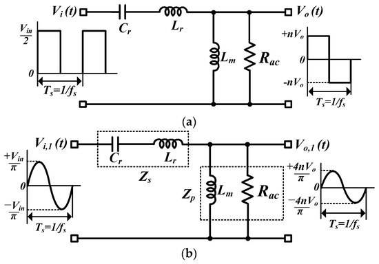
Figure 5.
Equivalent circuits of the proposed resonant converter. (a) AC equivalent circuit, (b) simplified equivalent circuit for FHA.
The DC voltage gain M of the proposed double LLC tank converter can be expressed as
where the inductor ratio , quality factor Q, and normalized switching frequency fn can be expressed as
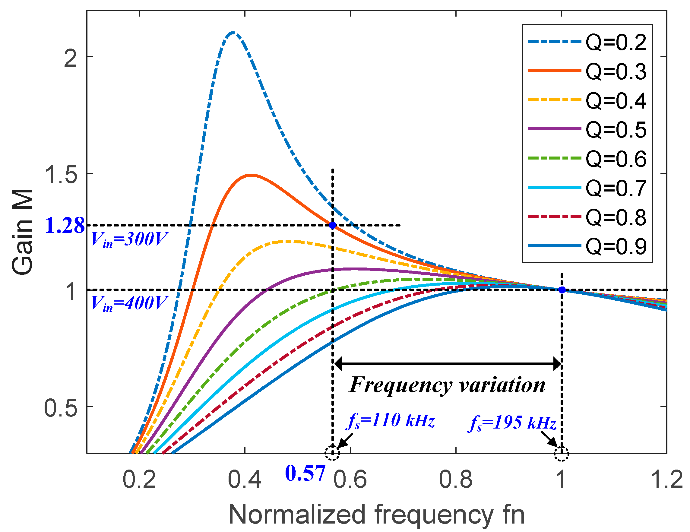
The curves of the DC voltage gain against the normalized frequency at different Q values and with Ln = 3.5 are shown in Figure 6, which is based on the experimental parameters. To ensure the ZVS operation of the proposed converter, it must be operated in the negative slope region of the voltage gain curves. The proposed converter has unity gain when the switching frequency is equal to the resonant frequency. The voltage gain increases when the switching frequency is lower than the resonant frequency. As can be seen from the graph, when the input voltage decreases from 400 V to 300 V, the switching frequency is lowered from 195 kHz (fn = 1) to 110 kHz (fn = 0.57) to achieve a voltage gain of 1.28. As a result, the output voltage is maintained at a constant voltage (48 V) without being lowered.
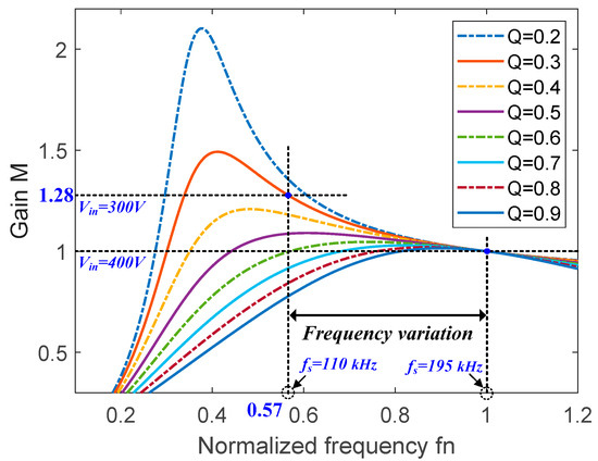
Figure 6.
The normalized DC voltage gain curves at different Q values with Ln = 3.5.
3.2. Input-Current Ripple
Figure 7 illustrates that the input-current ripple is caused by the difference between and when the L and C values of the resonance tanks are mismatched. In the proposed converter, if the waveforms of the resonant inductor currents iLr1 and iLr2 are the same, the input-current ripple theoretically becomes zero. To analyze the input-current ripple caused by the mismatched resonant elements, it is assumed that the two magnetizing inductances are equal, and the resonant capacitors and inductors are as follows:
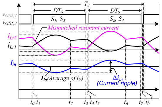
Figure 7.
Input-current ripple caused by the tolerances of the resonant elements.
The resonant inductor currents can be obtained as follows:
where
From (16) and (17), the input-current ripple can be obtained as follows:
From (19), it can be observed that if the tolerances a and b of Cr and Lr are within the ±2%, ±5%, and ±10% range, respectively, the input-current ripple occurs within approximately 10%, 20%, and 35%, respectively.
3.3. Comparison of Converter Circuit Topologies
A comparison of the proposed topology with other different topologies has been performed mainly in terms of the input-current ripple. The comparative results are presented in Table 1. The series resonant LC-DAB converter [21], using simple fixed-frequency modulation (FFM), can operate with ZVS and ZCS in a wide operating range, but it requires additional switches on its secondary side. In addition, TL LLC resonant converters [12,13,14] have the advantages of a soft-switching operation over a wide input voltage range and low-voltage stress on their switches. However, all circuit topologies mentioned above are buck-derived topologies with discontinuous input currents, which causes di/dt noise on the input side. On the other hand, although the proposed topology and HBC-CRR [19] are buck-derived converters, they have a continuous input current with low current ripple. However, the primary switches and secondary diodes in [19] operate under hard-switching conditions. In addition, for higher-voltage input applications, all the primary switches suffer from high-voltage stress. In contrast, the proposed converter improves the drawbacks of the hard-switching operation and high-voltage stress on the switches in [19].

Table 1.
Comparison of the proposed topology with other topologies.
4. Design Considerations
This section illustrates an example of the design of the proposed resonant converter, and particularly the design of the double LLC resonant tanks, which is based on the design specifications listed in Table 2.
Table 2.
Design specifications.
4.1. Transformer Turn Ratio
The proposed converter has unity gain at the maximum input voltage Vin(max), and its switching frequency is equal to the resonant frequency in the unity gain. The turn ratio of the transformer n can be obtained using Equation (13):
Thus, the transformer turn ratio n is approximately 2. Considering the magnetic core characteristics and turn ratio of the transformer, the number of turns in the primary and secondary windings of the transformer is selected to be 12 and 6, respectively.
4.2. Quality Factor
To simplify the design of the double LLC resonant tanks, Ln is selected to be 3.5. The available Q values are then limited to 0.53 to meet the condition of . As shown in Figure 6, the DC voltage gain M at Ln = 3.5 can be plotted based on these results. The DC voltage gain of the resonant tanks required to regulate the output voltage at the minimum input voltage Vin(min) and n = 2 is 1.28 according to (13). However, to prevent the converter from entering non-ZVS operation at Vin(min) and in the full-load condition, the required maximum gain of the resonant tanks should be sufficiently larger than 1.28. To achieve sufficient gain, the Q value of the resonant tank needs to be smaller, but a smaller Q value leads to higher current stress. Therefore, considering the sufficient gain and appropriate current stress of the resonant tanks, Q is selected to be 0.3.
4.3. Resonant Capacitor
The AC equivalent load Rac in the full-load condition is calculated as follows:
According to (14) and (21), the resonant capacitance can be obtained as
The maximum voltage of the resonant capacitor is given by
where ICr(pk) denotes the peak current of the resonant capacitor and fs denotes the switching frequency.
4.4. Resonant Inductor
From (14) and (22), the resonant inductance is obtained as
4.5. ZVS Conditions for Switches
The magnetizing inductance of the transformer Lm is 52.5 μH, which can be calculated from Lm = LnLr. The maximum magnetizing inductance for the ZVS can be calculated as
From (25), the maximum Lm for ZVS operation is about 260 μH. Considering that the magnetizing inductance is 52.5 μH, this is a reasonable value for the given input voltage range. Therefore, the main switches can be operated under ZVS conditions over a wide input voltage range.
5. Simulation and Experimental Results
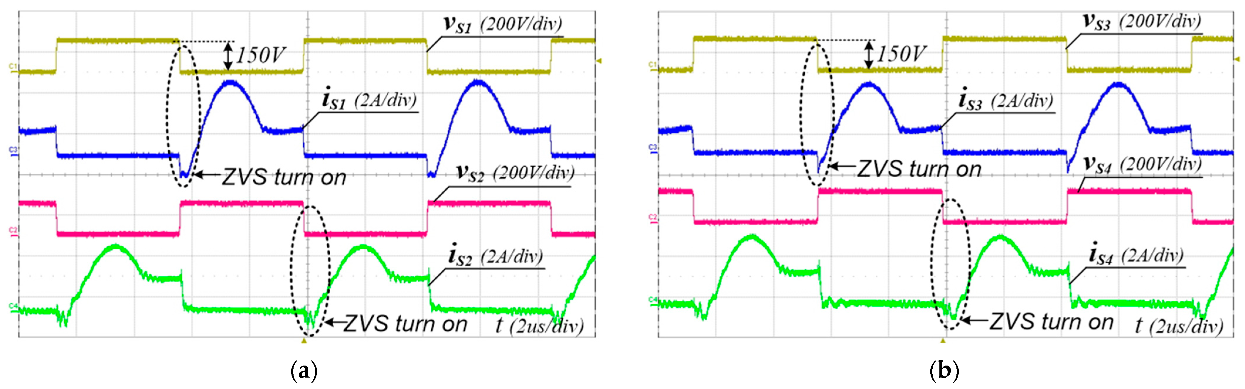
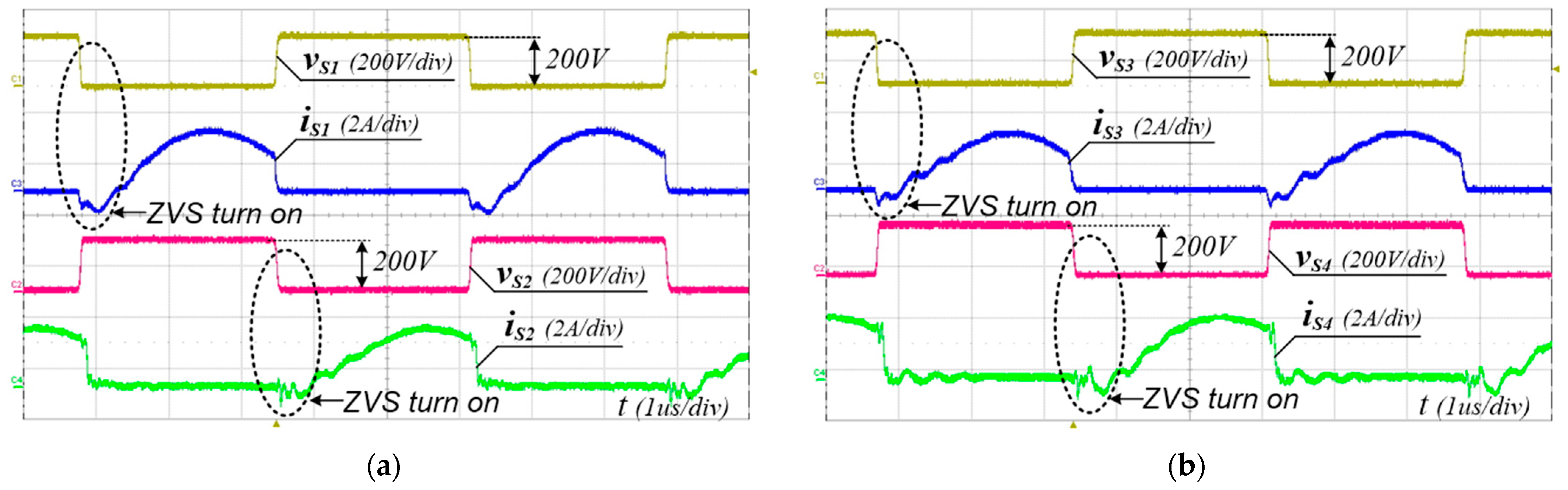
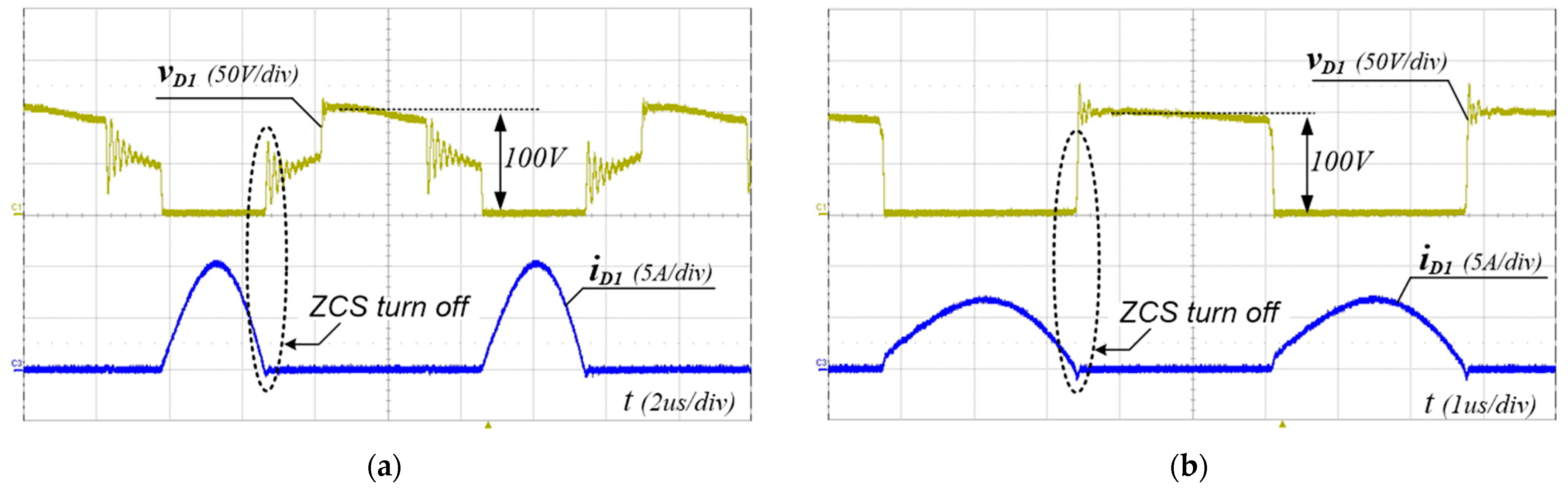
To verify the performance of the proposed converter, the 240 W prototype shown in Figure 8 has been built and tested. The PFM control of the proposed converter was implemented using a TI TMS320F28069M Digital MCU. The simulation and experimental parameters are listed in Table 3. The input voltage range and the output voltage were 300–400 V and 48 V, respectively. FQPF16N25 (250 V) MOSFETs with Si8261 gate drivers were used as the main switches. Figure 9, Figure 10 and Figure 11 show the experimental waveforms of the switches and diodes at input voltages of 300 V and 400 V, respectively. The switches and diodes operate with ZVS turn-on and ZCS turn-off, respectively, so no snubber is needed and the switching loss is improved. Moreover, as shown in Figure 10, the maximum switch voltage stress is about 200 V with no voltage spikes, which is half of the input voltage (400 V). This result indicates that the low-voltage-rated switches, 250 V and 500 V MOSFETs, can be used for 400 V and 800 V input applications, respectively. Figure 12a shows the experimental waveforms of the resonant tanks at Vin = 300 V. The resonant tanks operate well, which is in good agreement with our theoretical analysis. Figure 12b shows that when the values of Lr and Cr are mismatched with tolerances of about 5%, an input-current ripple of about 20% occurs without a pulsating shape, which is almost the same as the values analyzed in Section 3.2. Additionally, spike noises are observed in the input current, which occur due to current changes accompanying the turn-on and turn-off of main switches in current paths with parasitic inductances, especially during dead time. To reduce spike noise, parasitic inductances must be reduced. The dynamic response of the output voltage to load changes at the input voltages of 300 to 400 V is shown in Figure 13. The corresponding output voltage is well-regulated and stable in the dynamic load condition over a wide input voltage range when the load is changed stepwise from 20% to 100%. Figure 14 illustrates the simulated clamp-capacitor voltage imbalance with an input voltage. The two clamp capacitors are equally charged to half the input voltage if there is no voltage imbalance. The clamp-capacitor voltage imbalance mainly occurs when the resonant currents of the double LLC resonant tanks are imbalanced due to the tolerance of the Lr and Cr values of the resonant tanks, particularly at the minimum input voltage. When Lr and Cr values are mismatched with tolerances of ±10% and ±20%, the maximum imbalance of the clamp-capacitor voltage occurs at about 6.6% and 13.3% at the minimum input voltage of 300 V, respectively. However, as the input voltage increases, the capacitor voltage imbalance decreases. The measured efficiency under different load conditions, with an input voltage of 300–400 V, is shown in Figure 15. A maximum efficiency of 94.63% is measured at a 400 V input and under full load conditions. As the input voltage decreases, the efficiency decreases, mainly because the circulating current increases.
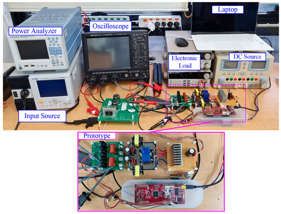
Figure 8.
Photograph of the experimental setup.
Table 3.
Experimental parameters.
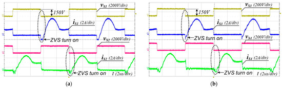
Figure 9.
Experimental voltage and current waveforms of switches at Vin = 300 V and Io = 5 A (full load). (a) S1 and S2, (b) S3 and S4.
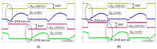
Figure 10.
Experimental voltage and current waveforms of switches at Vin = 400 V and Io = 5 A (full load). (a) S1 and S2, (b) S3 and S4.
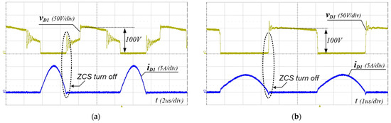
Figure 11.
Experimental voltage and current waveforms of Diode D1 at Io = 5 A (full load). (a) Vin = 300 V, (b) Vin = 400 V.
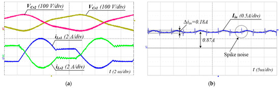
Figure 12.
Experimental waveforms at Vin = 300 V and Io = 5 A (full load). (a) Current and voltage of the resonant tanks, (b) input-current ripple.
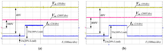
Figure 13.
The dynamic response of the output voltage with respect to load changes. (a) Vin = 300 V, (b) Vin = 400 V.

Figure 14.
Simulated clamp-capacitor voltage imbalance with input voltage.

Figure 15.
Measured efficiency curves of the proposed converter according to the output power.
6. Conclusions
A novel high-efficiency three-level double LLC resonant DC-DC converter with a ripple-free input current and low-voltage switch stress has been presented. The input noise components, which are due to the pulsating input current, can be significantly reduced without the addition of large input filters. Moreover, the voltage stress on the primary switches is only half the input voltage, which allows the proposed converter to use commercially available low-voltage-rated power switches for higher-voltage input applications. All the primary switches and secondary diodes are softly switched over a wide input voltage range, reducing switching loss. The advantages of the proposed converter mentioned above have been verified by the experimental results of a prototype converter with a 300–400 V input, 48 V/5 A output, and 195 kHz resonant frequency. The maximum efficiency of the proposed converter is about 94.63% under full load conditions at a 400 V input. As a result, since the proposed converter has the advantages of reduced input noise, low-voltage switch stress, and high efficiency, it is suitable for applications in DC-DC converters used in a DC microgrid with high-voltage DC bus.
Funding
This research received no external funding.
Data Availability Statement
The original contributions presented in this study are included in the article; further inquiries can be directed to the corresponding author.
Conflicts of Interest
The authors declare no conflict of interest.
References
- Khan, S.S.; Wen, H. A comprehensive review of fault diagnosis and tolerant control in DC-DC converters for DC micro grids. IEEE Access 2021, 9, 80100–80127. [Google Scholar] [CrossRef]
- Carvalho, E.L.; Sidorova, A.; Blinov, A.; Chub, A.; Vinnikov, D. Design considerations of dual-active bridge DC grid-forming converter for DC buildings. IEEE Trans. Ind. Electron. 2024, 71, 10601–10611. [Google Scholar] [CrossRef]
- Kakigano, H.; Miura, Y.; Ise, T. Low-voltage bipolar-type DC microgrid for super high quality distribution. IEEE Trans. Power Electron. 2010, 12, 3066–3075. [Google Scholar] [CrossRef]
- Stupar, A.; Friedli, T.; Minibock, J.; Kolar, J.W. Towards a 99% efficient three-phase buck-type PFC rectifier for 400-V DC distribution systems. IEEE Trans. Power Electron. 2012, 27, 1732–1744. [Google Scholar] [CrossRef]
- Sadaf, S.; Al-Emadi, N.; Maroti, P.K.; Iqbal, A. A New High Gain Active Switched Network-Based Boost Converter for DC Microgrid Application. IEEE Access 2021, 9, 68253–68265. [Google Scholar] [CrossRef]
- Lago, J.; Heldwein, M.L. Operation and control-oriented modeling of a power converter for current balancing and stability improvement of DC active distribution networks. IEEE Trans. Power Electron. 2011, 26, 877–885. [Google Scholar] [CrossRef]
- Pi, L.L. Modified Two-Channel LLC Resonant Converter With Optimal Efficiency for Wide Input Voltage Applications. IEEE Access 2023, 11, 38957–38969. [Google Scholar] [CrossRef]
- Zong, S.; Luo, H.; Li, W.; Deng, Y.; He, X. Asymmetrical Duty Cycle-Controlled LLC Resonant Converter with Equivalent Switching Frequency Doubler. IEEE Trans. Power Electron. 2016, 31, 4963–4973. [Google Scholar] [CrossRef]
- Cho, I.H.; Kim, Y.D.; Moon, G.-W. A Half-Bridge LLC Resonant Converter Adopting Boost PWM Control Scheme for Hold-Up State Operation. IEEE Trans. Power Electron. 2014, 29, 841–850. [Google Scholar] [CrossRef]
- Wang, H.; Chen, Y.; Fang, P.; Liu, Y.-F.; Afsharian, J.; Yang, Z. An LLC Converter Familiy with Auxiliary Switch for Hold-Up Mode Operation. IEEE Trans. Power Electron. 2017, 32, 4291–4306. [Google Scholar] [CrossRef]
- Jeong, Y.; Lee, M.-S.; Park, J.-D.; Kim, J.-K.; Rorrer, R.A.L. Holdup time compensation circuit of half-bridge LLC resonant converter for high light-load efficiency. IEEE Trans. Power Electron. 2020, 35, 13126–13135. [Google Scholar] [CrossRef]
- Jin, K.; Ruan, X. Hybrid full-bridge three-level LLC resonant converter—A novel dc–dc converter suitable for fuel-cell power system. IEEE Trans. Ind. Electron. 2006, 53, 1492–1503. [Google Scholar] [CrossRef]
- Gu, Y.; Lu, Z.; Hang, L.; Qian, Z.; Huang, G. Three-level LLC series resonant DC/DC converter. IEEE Trans. Power Electron. 2005, 20, 781–789. [Google Scholar] [CrossRef]
- Lee, I.-O.; Cho, S.-Y.; Moon, G.-W. Three-Level Resonant Converter with Double LLC Resonant Tanks for High-Input-Voltage Applications. IEEE Trans. Ind. Electron. 2012, 59, 3450–3463. [Google Scholar]
- Rathore, A.K.; Mazumder, S.K. Novel zero-current switching current-fed half-bridge isolated Dc/Dc converter for fuel cell based applications. In Proceedings of the 2010 IEEE Energy Conversion Congress and Exposition, Atlanta, GA, USA, 12–16 September 2010; pp. 3523–3529. [Google Scholar]
- Jang, S.J.; Chung-Yuen, W.; Byoung-Kuk, L.; Jin, H. Fuel cell generation system with a new active clamping current-fed half-bridge converter. IEEE Trans. Energy Convers. 2007, 22, 332–340. [Google Scholar] [CrossRef]
- Mousavi, A.; Das, P.; Moschopoulos, G. A comparative study of a new ZCS DC-DC full-bridge boost converter with a ZVS active-clamp converter. IEEE Trans. Power Electron. 2012, 27, 1347–1358. [Google Scholar] [CrossRef]
- Xin, Z.; Chung, H.S.H.; Xinbo, R.; Ioinovici, A. A ZCS full-bridge converter without voltage overstress on the switches. IEEE Trans. Power Electron. 2010, 25, 686–698. [Google Scholar]
- Leu, C.S.; Nha, Q.T. A Half-Bridge Converter With Input Current Ripple Reduction for DC Distribution Systems. IEEE Trans. Power Electron. 2013, 28, 1756–1763. [Google Scholar] [CrossRef]
- Kim, K.-M. High-Efficiency Resonant DC-DC Converter With Low Input Current Ripple for DC Power Distribution Systems. IEEE Access 2024, 12, 85983–85994. [Google Scholar] [CrossRef]
- Khan, D.; Hu, P.; Waseem, M.; Yasir Ali Khan, M.; Tahir, M.; Annuk, A. Practical Evaluation of Loss Reduction in Isolated Series Resonant Converter with Fixed Frequency Modulation. Energies 2022, 15, 5802. [Google Scholar] [CrossRef]


Disclaimer/Publisher’s Note: The statements, opinions and data contained in all publications are solely those of the individual author(s) and contributor(s) and not of MDPI and/or the editor(s). MDPI and/or the editor(s) disclaim responsibility for any injury to people or property resulting from any ideas, methods, instructions or products referred to in the content. |
© 2024 by the author. Licensee MDPI, Basel, Switzerland. This article is an open access article distributed under the terms and conditions of the Creative Commons Attribution (CC BY) license (https://creativecommons.org/licenses/by/4.0/).