Abstract
AlGaN/GaN high-electron-mobility transistors (HEMTs) with two different gate–drain distances (30 μm and 10 μm) were exposed to 1 MeV, 0.6 MeV, and 0.4 MeV protons at a fluence of 2.16 × 1012 cm−2. The gate–channel electron density and low-field mobility were obtained by measuring the capacitance–voltage characteristics and current–voltage characteristics. After proton irradiation, the gate–channel low-field electron mobility of the AlGaN/GaN HEMT with a 30 μm gate–drain distance increases and that with a 10 μm gate–drain distance decreases. It is studied and found that the mobility behavior is related to the polarization Coulomb field scattering, and the proton irradiation influences the intensity of the polarization Coulomb field scattering by changing the polarization/strain distribution in the barrier layer. The different gate–drain distances correspond to different variation trends of scattering intensity. The effect of 1 MeV protons on the barrier layer is smaller compared with 0.6 MeV and 0.4 MeV protons, so the mobility variation is smaller.
1. Introduction
AlGaN/GaN high-electron-mobility transistors (HEMTs) have the advantages of high breakdown voltage, high electron mobility, and high power density. They can work stably under harsh environments such as high temperature and high radiation due to the large band gap. Therefore, AlGaN/GaN HEMTs have broad application prospects in important fields such as radar communication, aerospace, and nuclear reactors [1,2,3,4,5,6].
Compared with Si- and GaAs-based devices, the better radiation resistance of AlGaN/GaN HEMTs has been proven theoretically [7,8]. However, during the growth process of the epitaxial layers, the lattice mismatch and thermal mismatch between the epitaxial layers induce a high density of defects [9,10]. It is a considerable challenge to the radiation resistance of AlGaN/GaN HEMTs in practical applications. In addition, as one of the main particles causing the degradation of the device performance in the radiation environment, the study of the proton irradiation of AlGaN/GaN HEMTs has received much attention. Hu et al. reported that the output characteristics and the transfer characteristics of the AlGaN/GaN HEMTs degraded slightly at the 15, 40, and 105 MeV proton irradiations, but the drain current and transconductance decreased by 10% and 6.1% for a 1.8 MeV fluence of 1012 cm−2, respectively [11]. The degradation of AlGaN/GaN HEMTs at different proton energies is consistent with the calculation of the non-ionizing energy loss. Kalavagunta et al. reported that the gate-lag of AlGaN/GaN HEMTs increases with a fluence increasing (from 3 × 1012 cm−2 to 3 × 1014 cm−2) at a 1.8 MeV proton irradiation [12]. Lv et al. studied the influence of 3 MeV protons on AlGaN/GaN HEMTs [13]. In addition, they observed that the drain saturation currents and maximum transconductance decreased by 20% and 5%, respectively. The degree of the threshold voltage shift increased with the proton fluence increasing. The density of vacancies at different proton fluences were calculated by using SRIM and adding the vacancies model into a Slivaco simulator. It is found that the result of the simulation is consistent with the experimental data and the Ga vacancies may be the main reason for the degradation of the AlGaN/GaN HEMTs’ performance. Ives et al. studied the effects of displacement damage induced by protons on AlGaN/GaN HEMTs [14]. The threshold voltage has a negative shift at a fluence of 1013 cm−2 and a positive shift at a high fluence of 1014 cm−2. It is attributed to the proton-induced donor defects (N vacancies) dominating at a low fluence and acceptor defects (Ga vacancies) dominating at a high fluence. Kim et al. studied the DC characteristic degradation of AlGaN/GaN HEMTs at the 0.5 MeV, 5 MeV, and 60 MeV proton irradiations, and the transfer characteristics at a 0.5 MeV proton irradiation has the most serious degradation. Moreover, the threshold voltage at the 0.5 MeV and 5 MeV proton irradiations has a positive shift, while the threshold voltage at a 60 MeV proton irradiation has a negative shift [15]. According to different scattering mechanisms, Tang et al. developed a model to simulate two-dimensional electron mobility at different proton energies and fluences at a low temperature [16]. It is found that the proton-induced ionized impurity scattering is the dominant factor in the degradation of electron mobility at a very low temperature (<5 K). The theoretical model of the proton irradiation effects on the two-dimensional electron density of AlGaN/GaN HEMTs were developed in the subsequent work [17]. The decrease of the electron density is a result of two mechanisms: the Fermi level is affected by the Ga vacancies in the GaN cap layer and AlGaN barrier layer, and the Ga vacancies in the GaN cap layer traps two-dimensional electrons in the potential well. These studies all consider that the displacement effect caused by proton irradiation is the main reason for the change of the AlGaN/GaN HEMTs’ performance. However, little attention has been paid to the proton influence on piezoelectric polarization.
For AlGaN/GaN HEMTs, the existence of two-dimensional electron gas (2DEG) in the channel depends on the spontaneous and piezoelectric polarization [18]. A change of the lattice structure, which is induced by the displacement effect, will inevitably affect the polarization charge distribution by changing the strain distribution. It has been proven that the polarization Coulomb field (PCF) scattering is a special and important scattering mechanism in AlGaN/GaN HEMTs, and the PCF scattering is directly related to the device size and polarization charge distribution at the AlGaN/GaN interface [19,20,21,22,23]. Therefore, proton irradiation will alter the electron mobility of AlGaN/GaN HEMTs and device performance through PCF scattering. Therefore, particular attention should be paid to the proton influence on PCF scattering.
In this paper, AlGaN/GaN HEMTs with two different gate–drain distances (30 μm and 10 μm) were prepared, which were irradiated with different proton energies (1 MeV, 0.6 MeV, and 0.4 MeV) at a fluence of 2.16 × 1012 cm−2. The capacitance–voltage (C–V) characteristics and current–voltage characteristics were measured before and after irradiation. The low-field electron mobility is extracted, the low-field electron mobility of the device with a 30 μm gate–drain distance gets increased, and that of the device with a 10 μm gate–drain distance gets decreased after proton irradiation. The degree of the low-field electron mobility variation decreases with the increase of proton energy. The proton irradiation effect on the two-dimensional electron transport properties is analyzed by using the theoretical model of PCF scattering related to the device size and polarization/strain distribution at the AlGaN/GaN interface.
2. Materials and Methods
Figure 1 shows the structure of AlGaN/GaN HEMTs in this study. The metal–organic chemical vapor deposition (MOCVD) was used to fabricate the AlGaN/GaN heterostructure material on Si substrate. The epitaxial layers are formed by 3.9 μm GaN buffer layer, 0.26 μm i-GaN layer, 27.5 nm Al0.25Ga0.75N barrier layer, and 3.3 nm GaN cap layer.
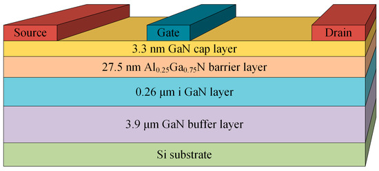
Figure 1.
Device structure of AlGaN/GaN HEMTs.
Source and drain are both Ohmic contacts and gate is Schottky contact. Gate–source distance LGS is 4 μm. Gate length LG is 4 μm, and gate width WG is 104 μm. The gate–drain distance LGD are 30 μm and 10 μm, which are marked as Device 1 and Device 2, respectively.
Proton irradiation was performed in a proton accelerator with the device temperature controlled at room temperature during irradiation. Devices were irradiated with 1 MeV, 0.4 MeV, and 0.6 MeV protons at a fluence rate of 108 cm−2/s. The proton irradiation lasted for 6 h, meaning a fluence of 2.16 × 1012 cm−2. The C–V characteristics and current–voltage characteristics were measured before and after proton irradiation.
3. Results and Discussion
Figure 2 shows the C–V curves of the AlGaN/GaN HEMTs measured at 1 MHz before and after proton irradiation. The C–V curve at 1 MHz reveals the information of 2DEG at the AlGaN/GaN interface. The gate–channel 2DEG electron density n2D can be obtained by the following equation [24]:
where C is the gate–source capacitance, VT is the threshold voltage, VGS is the gate–source voltage, M is the area of the gate Schottky contact, and e is the electron charge. VT is obtained by differentiating the C–V curve. Before irradiation, the VT values of Device 1 and Device 2 are both −4.95 V. After irradiation, the VT values of Device 1 are −4.95 V (1 MeV proton energy), −4.9 V (0.6 MeV proton energy), and −4.85 V (0.4 MeV proton energy). The VT values of Device 2 after irradiation are −4.95 V (1 MeV proton energy), −4.95 V (0.6 MeV proton energy), and −4.85 V (0.4 MeV proton energy). The shift of VT is related to the electron density [25]. The obtained n2D is shown in Figure 3. It is found that the n2D of Device 1 and Device 2 decrease by different degrees after irradiation. Protons cause displacement damage at the AlGaN/GaN interface, which is the main reason for the decrease of the electron density [13]. The decrease in n2D is the most obvious after a 0.4 MeV proton irradiation. With proton energy increasing, the degree of decrease in electron density gradually gets smaller. The decrease after a 1 MeV proton irradiation is the least. It explains that the degree of threshold voltage shift increases as proton energy decreases.
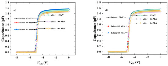
Figure 2.
Measured C–V curves before and after proton irradiation for Device 1 (a) and Device 2 (b).
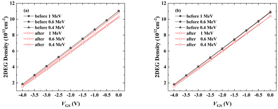
Figure 3.
Gate–channel 2DEG electron density n2D as a function of gate voltage for Device 1 (a) and Device 2 (b).
Figure 4 and Figure 5 are the IDS–VDS curves of Device 1 and Device 2 before and after proton irradiation. IDS and VDS are the drain-source current and drain-source voltage, respectively. It is found that the IDS of Device 1 increases and IDS of Device 2 decreases after 0.4 MeV irradiation. With proton energy increasing, the difference in the IDS between Device 1 and Device 2 is gradually disappearing. IDS is dominated by both electron density and electron mobility. The electron density of Device 1 and Device 2 both decrease after irradiation (Figure 3), and it cannot explain the increase of IDS in Device 1 (Figure 4c). Thus, the difference in the IDS between Device 1 and Device 2 should be induced by electron mobility. According to the IDS–VDS curves, the gate–channel 2DEG electron mobility μn is obtained as follows [24,26,27,28]:
where Rd is the gate–drain access resistance, Rs is the gate–source access resistance, Rc = 3.54 Ω∙mm is the Ohmic contact resistance, which is obtained by the transmission line method (TLM), and n2D0 and μn0 are the gate–channel 2DEG electron density and mobility corresponding to VGS = 0 V. The values of IDS at VDS = 0.1 V are adopted corresponding to the low-field region [27,28,29].
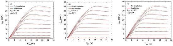
Figure 4.
Measured IDS–VDS curves of Device 1 before (“Pre-irradiation”) and after (“Irradiation”) proton irradiation with 1 MeV (a), 0.6 MeV (b), and 0.4 MeV (c) proton energies.
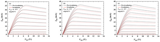
Figure 5.
Measured IDS–VDS curves of Device 2 before (“Pre-irradiation”) and after (“Irradiation”) proton irradiation with 1 MeV (a), 0.6 MeV (b), and 0.4 MeV (c) proton energies.
Figure 6 and Figure 7 show the μn of Device 1 and Device 2 before and after proton irradiation. In order to provide a clear comparison, the average change rates of μn for Device 1 and Device 2 under the 1 MeV, 0.6 MeV, and 0.4 MeV proton irradiations are given in Table 1. After a 0.4 MeV proton irradiation, the μn of Device 1 increases by 14.3% (Figure 6c) and that of Device 2 decreases by 15.0% (Figure 7c). As the proton energy increases, the magnitude of the μn variation for Device 1 and Device 2 gradually decrease. After a 1 MeV proton irradiation, there is a slight increase (+5.4%) in the μn of Device 1 (Figure 6a) and a slight decrease (−5.4%) in the μn of Device 2 (Figure 7a). It is found that the electron mobility varies differently between the devices with two different gate–drain distances and the magnitude of the variation decreases with the proton energy increasing. This μn behavior is explained as follows.
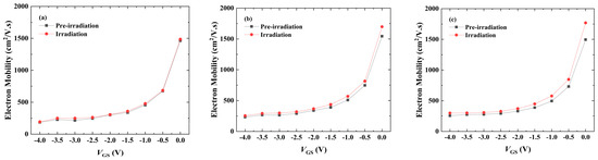
Figure 6.
Gate–channel low-field electron mobility μn of Device 1 before (“Pre-irradiation”) and after (“Irradiation”) proton irradiation as a function of gate voltage with 1 MeV (a), 0.6 MeV (b), and 0.4 MeV (c) proton energies.
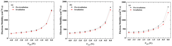
Figure 7.
Gate–channel low-field electron mobility μn of Device 2 before (“Pre-irradiation”) and after (“Irradiation”) proton irradiation as a function of gate voltage with 1 MeV (a), 0.6 MeV (b), and 0.4 MeV (c) proton energies.

Table 1.
Average change rate of μn for Device 1 and Device 2 with 1 MeV, 0.6 MeV, and 0.4 MeV protons.
In AlGaN/GaN HEMTs, electron mobility is mainly determined by the polar optical phonon (POP) scattering, acoustic phonon (AP) scattering, interface roughness (IFR) scattering, dislocation (DIS) scattering, and PCF scattering [29,30,31]. The first four scattering mechanisms are determined by the inherent properties of the AlGaN/GaN material and are not affected by the device size [20,31,32]. The devices in this study are fabricated on the same heterostructure material, so the first four scattering mechanisms of Device 1 are consistent with that of Device 2. Since the protons are uniformly irradiated over the devices, the variations of the inherent properties are the same for Device 1 and Device 2 under the same irradiation environment. For devices in the same proton irradiation environment, the variation of μn should be consistent under the influence of the first four scattering mechanisms after proton irradiation, which is inconsistent with the experimental results (Figure 6 and Figure 7). Previous studies have reported that PCF scattering is closely related to device size [19,20,21,22,23,28,29]. Therefore, although μn is dominated by POP scattering at room temperature, the differences in μn behavior corresponding to the different LGD (Figure 6 and Figure 7) must be attributed to PCF scattering.
Before device fabrication, the polarization charges in the heterostructure material are uniformly distributed. The device fabrication processing (rapid thermal annealing) and gate bias cause the nonuniform distribution of polarization charges at the AlGaN/GaN interface [24,29]. The PCF scattering of the AlGaN/GaN HEMTs originates from the difference between the nonuniform polarization charges and the uniform polarization charges, which is defined as the additional polarization charges ∆σ. Figure 8 is the ∆σ distribution diagram. The influence of the additional polarization charges near the Ohmic contact is negligible, considering that LGS and LGD are large enough and μn before irradiation is almost the same (Figure 6 and Figure 7) [29]. Therefore, the distribution of ∆σ is mainly divided into two parts, as shown in Figure 8. In region I, which is influenced by the converse piezoelectric effect, the negative gate bias compresses the lattices and the polarization charges decrease, generating the negative additional polarization charges ∆σ1. Due to the lattice continuity, the compression of the lattices in region I causes the tensile strain of the adjacent lattices in region II and the polarization charges increase, generating the positive additional polarization charges ∆σ2 [18,28]. The tensile effect weakens with the distance increasing, so the additional polarization charges in region II are linearly distributed. In addition, although LGS is different from LGD, the interaction effect of region I is the same for both the gate–source region and gate–drain region, and the effect of protons on the gate–source region and gate–drain region is also the same. For a clearer presentation and ease of understanding, the additional polarization charges of the gate–source region are treated the same as that of the gate–drain region. With this distribution of the additional polarization charge, the PCF scattering potential V(x,y,z) generates the following [29]:
where εs is the GaN dielectric constant. It is found from Equation (5) that the PCF scattering intensity is closely related to the device size and ∆σ distribution.
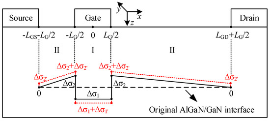
Figure 8.
Distribution of additional polarization charges at AlGaN/GaN interface.
Based on Figure 3, the level of the n2D variation ∆n2D after proton irradiation at VGS = 0 V as a function of proton energy is obtained and is shown in Figure 9. Since the 2DEG of the AlGaN/GaN HEMTs is determined by the strain and polarization, the n2D variation after proton irradiation indirectly reflects the lattice strain and polarization of region I, and the increase/decrease of the electron density corresponds to the enhanced/weakened tensile strain [18,33,34]. It is found from Figure 9 that the n2D of both Device 1 and Device 2 decrease, and the ∆n2D of Device 1 is larger than that of Device 2. This means that the tensile strain in region I is weakened after proton irradiation. In addition, the weakening amplitude of Device 1 is greater than that of Device 2. A previous study has reported that the effects of protons on the AlGaN/GaN heterostructure material are the ionization effect and displacement effect [35]. The ionization effect is the proton interaction with the lattice electrons, and the displacement effect is protons forcing atoms to leave the original lattice position [35]. The ionization effect will not change the lattice structure, so the change of the strain and polarization is caused by the displacement effect. Due to the same structure and size of the Schottky gates, at the same proton energy, the proton effect on region I should be the same for Device 1 and Device 2. Device 1 and Device 2 differ only in the gate–drain distance, so the variation of the tensile strain in region I must be attributed to the indirect effect of the adjacent region II. Since region I is covered by the gate metal, which has a blocking effect on protons, the proton irradiation effect of region I is different from that of region II. This makes the proton irradiation effect on the strain/polarization distribution of region I and region II different. Moreover, the PCF scattering is directly related to the nonuniform polarization charge distribution. Therefore, the main focus of this study is on the difference of the polarization distribution brought by proton irradiation for region I and region II. The enhancement of the tensile strain in region II can be inferred from the weakened tensile strain in region I. Compared with Device 2, the enhancement of the tensile strain in region II of Device 1 is greater, considering the greater weakening of the tensile strain in region I. The positive additional polarization charges ∆σ2’ is added to ∆σ2 due to the enhanced tensile strain in region II (Figure 8). In addition, since ∆σ is the additional polarization charges per unit area, and protons are uniformly irradiated on the devices, ∆σ2’ is the same in Device 1 and Device 2. The enhanced tensile strain in region II weakens the tensile strain in region I because of the lattice continuity, generating the extra negative additional polarization charges ∆σ1’ (Figure 8). According to Equation (5), the additional polarization charges in region I and region II have an offsetting effect, which affects the PCF scattering potential. A larger LGD will correspond to a stronger offsetting effect. For Device 1, the offset of ∆σ2 + ∆σ′ to ∆σ1 + ∆σ1′ is stronger due to the larger LGD. According to Equation (5), the PCF scattering potential becomes weaker and μn gets larger after proton irradiation (Figure 6). For Device 2, LGD is smaller, which corresponds to a smaller integration interval of the last term in Equation (5). In addition, the offset of ∆σ2 + ∆σ2′ to ∆σ1 + ∆σ1′ is weaker. Therefore, ∆σ1 + ∆σ1′ plays a dominant role at this point, enhancing the PCF scattering potential and causing a decrease in the μn after proton irradiation (Figure 7).
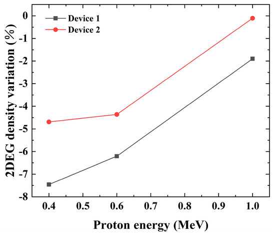
Figure 9.
Level of the 2DEG electron density variation after proton irradiation at gate–source voltage VGS = 0 V as a function of proton energy.
The action distance of higher energy protons is farther from the barrier layer, and with the proton energy increasing, the non-ionizing energy transferred from the proton to the atom decreases, which causes the degree of displacement damage to decrease [35,36]. This is the reason that the action intensity of higher energy protons on the barrier layer is lower in a certain energy range. It is found from Figure 9 that the amplitude of the n2D variation decreases with increasing proton energy. This indicates that the weakening degree of the tensile strain in region I gradually decreases as the proton energy increases. In other words, the enhancement degree of the tensile strain in region II gradually decreases. Therefore, for devices with the same LGD, the absolute value of ∆σ2′ decreases with the increasing proton energy, and the absolute value of ∆σ1′ decreases simultaneously. For Device 1 at a 1 MeV proton irradiation, the influence of ∆σ2 + ∆σ2′ is weaker than that at a 0.4 MeV proton irradiation. Following Equation (5), the decrease degree of the PCF scattering potential gets lower with the proton energy increasing. As a result, compared with Figure 6c, the increase of μn is smaller in Figure 6a. For Device 2 at a 1 MeV proton irradiation, ∆σ1 + ∆σ1′ plays a dominant role. With the proton energy increasing, the absolute value of ∆σ1′ decreases, and the PCF scattering potential gets lower. This makes the decrease degree of μn smaller in Figure 7a, compared with Figure 7c.
4. Conclusions
Based on the PCF scattering theory, the proton irradiation effect on the transport characteristics of AlGaN/GaN HEMTs is analyzed in terms of the gate–drain distance and proton energy. It is found that the displacement damage caused by protons changes the polarization/strain distribution at the AlGaN/GaN interface, which affects the 2DEG electron density and intensity of the PCF scattering. Due to the displacement damage, the electron density decreases after proton irradiation. In addition, the decrease degree of the device with a large gate–drain distance is larger. The electron mobility of the device with a large gate–drain distance increases after irradiation due to the weakening of the PCF scattering. For the device with a small gate–drain distance, the electron mobility decreases after irradiation due to the enhancement of the PCF scattering. The change of the electron mobility is the main reason for the difference in the output current. The impact of proton irradiation on the electrical performance gradually decreases with the proton energy increasing. Although the electron density decreases after a 0.4 MeV proton irradiation, the current and low-field electron mobility of the device with a larger gate–drain distance increase. Thus, the proton effect and gate–drain distance can be adjusted appropriately to improve the device performance. Moreover, based on a theoretical model of the PCF scattering, the variation of the strain at the AlGaN barrier layer is obtained by an analysis of the electrical properties. It is helpful to understand the mechanism of the proton irradiation influence on AlGaN/GaN HEMTs at the microscopic level. This is beneficial for improving the irradiation resistance of AlGaN/GaN HEMTs in the field of aerospace.
Author Contributions
Conceptualization, Q.J. and M.Y.; investigation, Q.J. and X.H.; methodology, Q.J. and M.Y.; writing—original draft, Q.J.; writing—review and editing, J.L. and M.Y.; supervision, G.W. and M.Q.; project administration, S.L. All authors have read and agreed to the published version of the manuscript.
Funding
This work was supported by the National Natural Science Foundation of China (Grant No. 61904007).
Data Availability Statement
The data that support the findings are available from the corresponding author upon reasonable request.
Conflicts of Interest
The authors declare that they have no known competing financial interests or personal relationships that could have appeared to influence the work reported in this paper.
References
- Nguyen, H.Q.; Nguyen, T.; Tanner, P.; Nguyen, T.K.; Foisal, A.R.M.; Fastier-Wooller, J.; Nguyen, T.H.; Phan, H.P.; Nguyen, N.T.; Dao, D.V. Piezotronic effect in a normally off p-GaN/AlGaN/GaN HEMT toward highly sensitive pressure sensor. Appl. Phys. Lett. 2021, 118, 242104. [Google Scholar] [CrossRef]
- Narang, K.; Bag, R.K.; Singh, V.K.; Pandey, A.; Saini, S.K.; Khan, R.; Arora, A.; Padmavati, M.V.G.; Tyagi, R.; Singh, R. Improvement in surface morphology and 2DEG properties of AlGaN/GaN HEMT. J. Alloys Compd. 2020, 815, 152283. [Google Scholar] [CrossRef]
- Moon, J.S.; Wong, J.; Grabar, B.; Antcliffe, M.; Chen, P.; Arkun, E.; Khalaf, I.; Corrion, A.; Chappell, J.; Venkatesan, N.; et al. 360 GHz fMAX graded-channel AlGaN/GaN HEMTs for mmW low-noise applications. IEEE Electron Device Lett. 2020, 41, 1173–1176. [Google Scholar] [CrossRef]
- Pengelly, R.S.; Wood, S.M.; Milligan, J.W.; Sheppard, S.T.; Pribble, W.L. A Review of GaN on SiC High Electron-Mobility Power Transistors and MMICs. IEEE Trans. Microw. Theory Tech. 2012, 60, 1764–1783. [Google Scholar] [CrossRef]
- Chen, K.J.; Haberlen, O.; Lidow, A.; Tsai, C.L.; Ueda, T.; Uemoto, Y.; Wu, Y. GaN-on-Si power technology: Devices and applications. IEEE Trans. Electron Devices 2017, 64, 779–795. [Google Scholar] [CrossRef]
- Pearton, S.J.; Ren, F.; Patrick, E.; Law, M.E.; Polyakov, A.Y. Ionizing radiation damage effects on GaN devices. ECS J. Solid State Sci. Technol. 2016, 5, Q35. [Google Scholar] [CrossRef]
- Ionascut-Nedelcescu, A.; Carlone, C.; Houdayer, A.; von Bardeleben, H.J.; Cantin, J.; Raymond, S. Radiation hardness of gallium nitride. IEEE Trans. Nucl. Sci. 2002, 49, 2733–2738. [Google Scholar] [CrossRef]
- Abderrahmane, A.; Koide, S.; Tahara, T.; Sato, S.; Ohshima, T.; Okada, H.; Sandhu, A. Effect of proton irradiation on 2DEG in AlGaN/GaN heterostructures. J. Phys. Conf. Ser. 2013, 433, 12011. [Google Scholar] [CrossRef]
- Binari, S.C.; Klein, P.B.; Kazior, T.E. Trapping effects in GaN and SiC microwave FETs. Proc. IEEE 2002, 90, 1048–1058. [Google Scholar] [CrossRef]
- Divay, A.; Latry, O.; Duperrier, C.; Temcamani, F. Ageing of GaN HEMT devices: Which degradation indicators? J. Semicond. 2016, 37, 14001. [Google Scholar] [CrossRef]
- Hu, X.; Bo, K.C.; Barnaby, H.J.; Fleetwood, D.M.; Schrimpf, R.D.; Lee, S.; Shojah-Ardalan, S.; Wilkins, R.; Mishra, U.K.; Dettmer, R.W. The energy dependence of proton-induced degradation in AlGaN/GaN high electron mobility transistors. IEEE Trans. Nucl. Sci. 2004, 51, 293–297. [Google Scholar] [CrossRef]
- Kalavagunta, A.; Silvestri, M.; Beck, M.J.; Dixit, S.K.; Schrimpf, R.D.; Reed, R.A.; Fleetwood, D.M.; Shen, L.; Mishra, U.K. Impact of proton irradiation-induced bulk defects on gate-lag in GaN HEMTs. IEEE Trans. Nucl. Sci. 2009, 56, 3192–3195. [Google Scholar] [CrossRef]
- Lv, L.; Ma, J.G.; Cao, Y.R.; Zhang, J.C.; Zhang, W.; Li, L.; Xu, S.R.; Ma, X.H.; Ren, X.T.; Hao, Y. Study of proton irradiation effects on AlGaN/GaN high electron mobility transistors. Microelectron. Reliab. 2011, 51, 2168–2172. [Google Scholar] [CrossRef]
- Ives, N.E.; Chen, J.; Witulski, A.F.; Schrimpf, R.D.; Fleetwood, D.M.; Bruce, R.W.; McCurdy, M.W.; Zhang, E.X.; Massengill, L.W. Effects of proton-induced displacement damage on gallium nitride HEMTs in RF power amplifier applications. IEEE Trans. Nucl. Sci. 2015, 62, 2417–2422. [Google Scholar] [CrossRef]
- Kim, D.S.; Lee, J.H.; Kim, J.G.; Yoon, Y.J.; Lee, J.S.; Lee, J.H. Anomalous DC characteristics of AlGaN/GaN HEMTs depending on proton irradiation energies. ECS J. Solid State Sci. Technol. 2020, 9, 65005. [Google Scholar] [CrossRef]
- Tang, J.; Liu, G.; Zhao, G.; Xing, S.; Malik, S.A. Effect of proton irradiation on the mobility of two-dimensional electron in AlGaN/AlN/GaN high electron mobility transistors at low temperature. J. Vac. Sci. Technol. B 2020, 38, 23202. [Google Scholar] [CrossRef]
- Tang, J.J.; Liu, G.P.; Song, J.Y.; Zhao, G.J.; Yang, J.H. Analysis of the decrease of two-dimensional electron gas concentration in GaN-based HEMT caused by proton irradiation. Chin. Phys. B 2021, 30, 27303. [Google Scholar] [CrossRef]
- Ambacher, O.; Smart, J.; Shealy, J.R.; Weimann, N.G.; Chu, K.; Murphy, M.; Schaff, W.J.; Eastman, L.F.; Dimitrov, R.; Wittmer, L.; et al. Two-dimensional electron gases induced by spontaneous and piezoelectric polarization charges in N-and Ga-face AlGaN/GaN heterostructures. J. Appl. Phys. 1999, 85, 3222–3233. [Google Scholar] [CrossRef]
- Yuan, L.; Chen, H.; Chen, K.J. Normally off AlGaN/GaN metal–2DEG tunnel-junction field-effect transistors. IEEE Electron Device Lett. 2011, 32, 303–305. [Google Scholar] [CrossRef]
- Cui, P.; Liu, H.; Lin, W.; Lin, Z.; Cheng, A.; Yang, M.; Liu, Y.; Fu, C.; Lv, Y.; Luan, C. Influence of different gate biases and gate lengths on parasitic source access resistance in AlGaN/GaN heterostructure FETs. IEEE Trans. Electron Devices 2017, 64, 1038–1044. [Google Scholar] [CrossRef]
- Lv, Y.; Lin, Z.; Meng, L.; Luan, C.; Cao, Z.; Yu, Y.; Feng, Z.; Wang, Z. Influence of the ratio of gate length to drain-to-source distance on the electron mobility in AlGaN/AlN/GaN heterostructure field-effect transistors. Nanoscale Res. Lett. 2012, 7, 434. [Google Scholar] [CrossRef]
- Liu, Y.; Lin, Z.J.; Yang, M.; Luan, C.B.; Wang, Y.T.; Lv, Y.J.; Feng, Z.H. Effect of polarization Coulomb field scattering on low temperature electron mobility in strained AlGaN/AlN/GaN heterostructure field-effect transistors. Mod. Phys. Lett. B 2016, 30, 1650411. [Google Scholar] [CrossRef]
- Yang, M.; Ji, Q.; Su, X.; Zhang, W.; Wang, Y.; Wang, L.; Hu, X.; Yuan, Q.; Feng, P.; Liu, Y. Study on the electron mobility related with ohmic contact width in AlGaN/GaN HEMTs. Mod. Phys. Lett. B 2020, 34, 2150008. [Google Scholar] [CrossRef]
- Zhao, J.; Lin, Z.; Corrigan, T.D.; Wang, Z.; You, Z.; Wang, Z. Electron mobility related to scattering caused by the strain variation of AlGaN barrier layer in strained AlGaN/GaN heterostructures. Appl. Phys. Lett. 2007, 91, 173507. [Google Scholar] [CrossRef]
- Dongmin, K.; Hyungtak, K. Energy-Dependent Degradation Characteristics of AlGaN/GaN MISHEMTs with 1, 1.5, and 2 MeV Proton Irradiation. ECS J. Solid State Sci. Technol. 2018, 7, Q159–Q163. [Google Scholar]
- Yang, M.; Ji, Q.; Wang, Y.; Hu, X.; Yuan, Q.; Liu, X.; He, J.; Wang, R.; Zhou, L.; Xiao, J.; et al. Drain Schottky contact influence on low-field transport characteristic of AlGaN/GaN heterostructure field-effect transistors. Appl. Phys. A 2022, 128, 460. [Google Scholar] [CrossRef]
- Lv, Y.; Lin, Z.; Zhang, Y.; Meng, L.; Luan, C.; Cao, Z.; Chen, H.; Wang, Z. Polarization Coulomb field scattering in AlGaN/AlN/GaN heterostructure field-effect transistors. Appl. Phys. Lett. 2011, 98, 123512. [Google Scholar] [CrossRef]
- Yang, M.; Lv, Y.; Cui, P.; Liu, Y.; Fu, C.; Lin, Z. Determination of the polarization and strain distribution in AlGaN/GaN heterostructure field-effect transistors. J. Phys. Chem. Solids 2018, 123, 223–227. [Google Scholar] [CrossRef]
- Luan, C.; Lin, Z.; Lv, Y.; Zhao, J.; Wang, Y.; Chen, H.; Wang, Z. Theoretical model of the polarization Coulomb field scattering in strained AlGaN/AlN/GaN heterostructure field-effect transistors. J. Appl. Phys. 2014, 116, 44507. [Google Scholar] [CrossRef]
- Yang, M.; Lv, Y.; Feng, Z.; Lin, W.; Cui, P.; Liu, Y.; Fu, C.; Lin, Z. Study of source access resistance at direct current quiescent points for AlGaN/GaN heterostructure field-effect transistors. J. Appl. Phys. 2016, 119, 224501. [Google Scholar] [CrossRef]
- Gurusinghe, M.N.; Davidsson, S.K.; Andersson, T.G. Two-dimensional electron mobility limitation mechanisms in AlxGa1-xN/GaN heterostructures. Phys. Rev. B 2005, 72, 45316. [Google Scholar] [CrossRef]
- Yang, M.; Lin, Z.; Zhao, J.; Cui, P.; Fu, C.; Lv, Y.; Feng, Z. Effect of Polarization Coulomb Field Scattering on Parasitic Source Access Resistance and Extrinsic Transconductance in AlGaN/GaN Heterostructure FETs. IEEE Trans. Electron Devices 2016, 63, 1471–1477. [Google Scholar] [CrossRef]
- Ibbetson, J.P.; Fini, P.T.; Ness, K.D.; DenBaars, S.P.; Speck, J.S.; Mishra, U.K. Polarization effects, surface states, and the source of electrons in AlGaN/GaN heterostructure field effect transistors. Appl. Phys. Lett. 2000, 77, 250–252. [Google Scholar] [CrossRef]
- Goyal, N.; Iñiguez, B.; Fjeldly, T.A. Analytical modeling of bare surface barrier height and charge density in AlGaN/GaN heterostructures. Appl. Phys. Lett. 2012, 101, 103505. [Google Scholar] [CrossRef]
- Lv, L.; Zhang, J.C.; Li, L.; Ma, X.H.; Cao, Y.R.; Hao, Y. Effects of 3 MeV proton irradiations on AlGaN/GaN high electron mobility transistors. Acta Phys. Sinica 2012, 61, 57202. [Google Scholar]
- Sonia, G.; Richter, E.; Lossy, R.; Mai, M.; Schmidt, J.; Weyers, M.; Tränkle, G.; Denker, A.; Opitz-Coutureau, J.; Pensl, G.; et al. High and low energy proton irradiation effects on AlGaN/GaN HFETs. Phys. Stat. Sol. C 2006, 3, 2338–2341. [Google Scholar] [CrossRef]
Disclaimer/Publisher’s Note: The statements, opinions and data contained in all publications are solely those of the individual author(s) and contributor(s) and not of MDPI and/or the editor(s). MDPI and/or the editor(s) disclaim responsibility for any injury to people or property resulting from any ideas, methods, instructions or products referred to in the content. |
© 2023 by the authors. Licensee MDPI, Basel, Switzerland. This article is an open access article distributed under the terms and conditions of the Creative Commons Attribution (CC BY) license (https://creativecommons.org/licenses/by/4.0/).