Abstract
Stochastic Computing (SC) is an alternative way of computing with binary weighted words that can significantly reduce hardware resources. This technique relies on transforming information from a conventional binary system to the probability domain in order to perform mathematical operations based on probability theory, where smaller amounts of binary logic elements are required. Despite the advantage of computing with reduced circuitry, SC has a well known issue; the input interface known as stochastic number generator (SNG), is a hardware consuming module, which is disadvantageous for small digital circuits or circuits with several input data. Hence, in this work, efforts are dedicated to improving a classic weighted binary SNG (WBSNG). For this, one of the internal modules (weight generator) of the SNG was redesigned by detecting a pattern in the involved signals that helped to pose the problem in a different way, yielding equivalent results. This greatly reduced the number of logical elements used in its implementation. This pattern is interpreted with Boolean equations and transferred to a digital circuit that achieves the same behavior of a WBSNG but with less resources.
1. Introduction
Six decades ago, the pioneering work of Gaines [1] introduced a novel computation technique known as Stochastic Computing (SC) [2,3]. This technique relies on a data domain transformation, i.e., from a weighted binary system (WBS) to an unary system, where the resulting number is a string of 0’s and 1’s, with the property that the percent of 1’s in the string represents the value of the number as a probability; hence, the string is known as probabilistic sequence (PS) or probabilistic sequence, and the input transforming circuit is known as Stochastic Number Generator (SNG). Each bit is assumed to be random, i.e., the bits at different positions are uncorrelated [4]. Due to the fact that the interaction between classic probabilistic sets can be set up with logical operators, working with probabilistic sequences makes it possible to rely on single logical gates for implementing math operations, resulting in smaller digital circuit designs than those obtained with the corresponding counterpart based on a WBS. Once results are obtained, data are back-transformed to a WBS by means of a counter, i.e., by counting the 1’s in the PS. It is worth mentioning that the available computational resources at the time that Gaines proposed the SC were limited, making SC unfeasible. Figure 1 shows a block diagram of a stochastic computing system where domain transformation elements are evident.
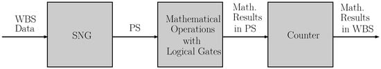
Figure 1.
Block diagram of a stochastic computing system.
One of the most attractive features of stochastic computing is the great reduction in logic elements or gates for the design of specific applications, since basically the format in which the numbers work has the property of randomness and depends on the probabilistic mathematical operations that can be performed between them and that can be implemented with simple logic gates. On the other hand, fault tolerance is one of the advantages of stochastic computing [5], since the impact due to the bit flip or soft error phenomenon (so called because it is a transient error and is not related to physical damage to the device; it only causes the change in an arbitrary bit [6]) has less impact because the bits in an PS are not weighted. In terms of applications, SC is useful where small errors are tolerated, such as image processing [7] and neural networks [8], although there are also more specific and unconventional applications, such as the design of automatic controllers [9].
Advancements in digital devices technology have rendered cheaper, simpler and more flexible implementations of algorithms based on SC as in [10], where a standalone SC architecture that can perform accurate arithmetic operations such as addition, subtraction, multiplication and sorting was designed as in-memory SC architecture based on 2D memtransistors. But in general, there is a drawback presented by SC; i.e., an n-bit binary number can represent up to levels, but in order to deal with the same resolution in SC, a string of bits is required, which considerably increases latency, making the SC match low-speed applications as artificial neural networks, as decoding low-density parity check codes and polar codes, for digital filters, among others [4].
Nowadays, due to the recent available computational power in digital devices as FPGAs [11] and due to other great features of SC techniques such as error resilience, low power consumption and low resource arithmetical unit implementations, researchers in different areas are thoroughly exploring this computation technique again [5,12]. Nevertheless, drawbacks are still present in SC, such as the loss of accuracy in relatively large circuits, restrict the SC to small algorithms. Another important drawback is resource consumption by the SNG. Each involved signal must be transformed by an SNG; hence, it is possible that all the circuits involved in SNGs are larger than the stochastic digital circuit itself, clearly losing the advantage of smaller circuit designs in the stochastic domain. The reason for this fact is that the SNG consists of two parts: a Linear Feedback Shift Register (LFSR) that generates a Pseudo-Random Binary Signal (PRBS) [13] and a comparator.
Recently, some researchers have focused their efforts on novel applications of SC, e.g., control algorithms [9], deep learning [14], machine learning [15] and estimation algorithms [16], just to mention a few. Other researchers are concerned with the disadvantages of SC, hence aiming their research at alleviating SC drawbacks; e.g., in [17], an area-efficient SNG by sharing the permuted output of one LFSR among several SNGs is proposed; despite novelties presented in this work using permuted readings to obtain more stochastic sequences, it just avoids the implementation of more LFSRs, which is attractive, but the SNG is not only composed of LFSRs, but of a comparator too. Precision degradation in subsequent phases after the application of the method to select permuted pairs is still a risk.
SNGs can be divided into two types: True SNG (TSNG) and Pseudo-Random Number Generator (PRNG). TSNG has a natural source of randomness to seed the comparator generating outputs. Through the years, one of the most outstanding developments of this type of SNG has been spintronic devices such as the one presented in [18], where a scalable SNG based on the Spin–Hall effect is proposed, which is capable of generating multiple independent stochastic streams simultaneously. The design takes advantages of the efficient charge-to-spin conversion from the Spin–Hall material and the intrinsic stochasticity of nano-magnets; although the proposal shows interesting results, it is not of practical use as it requires custom non-commercial semiconductor devices also. Previous works [5] have concluded that SNGs that truly use randomness as presented in [18] can result in worse results than those obtained with PRNG ones. One of the reasons could be that the maximum length for the PS is not guaranteed with such semiconductor devices. SNG based on spintronic devices as an n-bit random number generator still relies on the conventional SNG main idea: comparison of a number to obtain a PS. Therefore, the chance of losing accuracy sooner in a large system implementation using spintronic devices is higher than that obtained with conventional SNG based on LFSR. On the other hand, PRNGs are not fundamentally based on a natural randomness phenomena, but as was mentioned before, PRNGs are more accurate than TSNG. Most of the PRNGs, at least the most popular, are based on LFSR designs; others are based on quasi random number generators known as low-discrepancy (LD) sequences or Sobol sequence generators [19], based on the Least Significative Zero detection from a counter. Generating this kind of LD sequences has been proposed to improve the accuracy and computation speed of stochastic computing circuits. Nevertheless, the large amount of hardware for Sobol sequence generators makes them expensive in terms of area and energy consumption. In [20], two minimum probability-conversion circuits (MPCC) are proposed for reducing the hardware cost of SNGs, the MPCC of two-level logic (MPCC-2L) design and the MPCC of multilevel logic (MPCC-ML) design. The authors claim the MPCC-2L design slightly reduces SNG hardware cost, but the MPCC-ML design significantly reduces hardware cost as much as for a 10-bit word. True results for the MPCC-ML are not presented since the authors state that additional flip-flops are required in between multiple levels of logic.
It is clear that there are opportunities for solving drawbacks in SC and in particular the issue with the SNG, i.e., its circuitry has the disadvantage of being relatively large, is attractive for investigating an alternative digital circuit proposal with less hardware. To the authors’ best knowledge, there are more PRNG works than TSNG in the literature due to some arguments given above.
Hence, this work contributes with the proposal of a novel SNG of the pseudo-random type that requires fewer logic gates. This is possible due to the structure of the comparator inside the SNG, in which some patterns were detected in the transformation process from WBS to PS, yielding in that way to a simpler digital circuit that represents such patterns with respect to the one in a classic SNG [21] currently in use by engineers (see Remark 1).
Remark 1.
Although the generator is somewhat old, it is still used by engineers, as can be seen in references [22,23,24]. Its popularity is due to the fact that it has the unique property of generating low-correlation sequences that perform accurate multiplications; hence, new proposals are still taking advantage of this property, as in [17,25]. It is worth mentioning that to the best of the authors’ knowledge, this generator has never been reduced, with the exception of the work [20]. Therefore, it is of interest to be able to make improvements to this generator to allow future works to have an economical and updated version of it.
2. Stochastic Computing Principles
Let () be a number represented in an n-bit WBS format, transformed into a probabilistic sequence denoted by X. For that, the number needs to be normalized, i.e., , with x as the normalized number and ; hence, and it relates to X with being the probability of 1’s appearing in the PS X, permitting the binary sequences to compute with them in a probabilistic fashion. This fact is possible because a PS is the accumulation of 1’s and 0’s in a period , which is permeated with random properties due to transformation; hence, it allows probabilistic computations. From this perspective, logical gates are treated as probabilistic experiments.
2.1. Basic Arithmetic Operations
Let be a PS input for and Y be a PS output; then, their corresponding probabilities of 1’s appearing in the PS are and , respectively. These probabilities are related to numerical values corresponding to a PS of the following form: , . Assume that and are uncorrelated, with and . Now, the intersection of two sets is solved with a multiplication,
It is clear that ; therefore, dealing with PSs, multiplication is carried out with an AND gate, as illustrated in Figure 2.
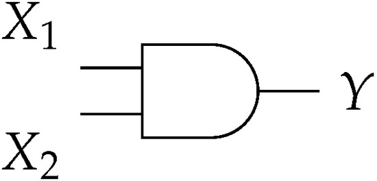
Figure 2.
AND gate as a multiplication operator of PSs.
The union of two sets is as follows:
which corresponds to the logical gate OR, as illustrated in Figure 3.
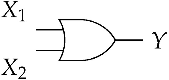
Figure 3.
OR gate implementing the operation with PSs.
The logic gate NOT as shown in Figure 4 is interpreted in the following form:
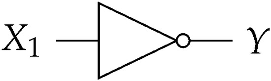
Figure 4.
NOT gate implementing the operation with PSs.
To keep the results within the range , a scaled addition is needed, and for that, a multiplexer is considered, as shown in Figure 5.
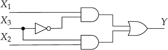
Figure 5.
Multiplexer for scaled addition, where , are inputs, is the selector and Y is the output.
Now, by choosing , Equation (4) yields to:
and ; therefore, in SC, addition is carried out with a multiplexer with an even selection, as shown in Figure 6.
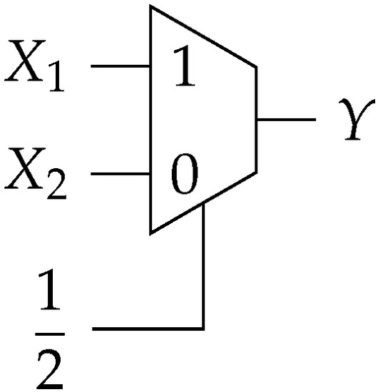
Figure 6.
Multiplexer as a scaled addition of PSs.
The logic gate XNOR as shown in Figure 7 can be analyzed in a similar fashion as the multiplexer (see for instance [26]); hence, it is interpreted as the following form:
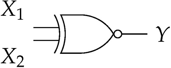
Figure 7.
XNOR gate implementing the operation with PSs.
As an example, let us consider a function where its corresponding implementation with SC techniques is shown in Figure 8. It is clear that , , , and that the output of the AND gate can be computed for two different forms: with the probabilistic values at the inputs, i.e., and by proceeding bit by bit, where the resulting PS agrees with . Finally, the probabilistic values at the input of the multiplexer are and and for the selector ; hence, the output is determined as . This result agrees with .
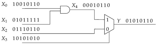
Figure 8.
Stochastic circuit for implementing function .
In the example of Figure 8, it is clear that the 3-bit input data are converted by means of an SNG to a PS, where the zero state was artificially added in the LFSR, hence yielding 8-bit long PSs. See, for instance, Remark 2.
Remark 2.
For the sake of simplicity, in this work, only the unipolar format is considered. For dealing with SC based on bipolar or hybrid formats, the reader can consult the work [27].
2.2. Domain Transformations
2.2.1. From WBS to PS
The SNG has two main modules:
- (a)
- LFSR:The LFSR consists of Flip-Flops (FFs) in a cascade interconnection. The LFSR is characterized by a feedback from some memory elements through a Modulo-2 adder (XOR gates) to the first FF. There are several feedback combinations from the memory elements. Some combinations will make the LFSR generate the largest output sequences. In general, for an n-bit LFSR, the maximum length of a sequence (period) is given by (the subtraction of 1 is due to the fact that the LFSR cannot generate the zero state). Other combinations will make the LFSR generate short output sequences, where its length can be an integer common multiple of [28].
- (b)
- Comparator:This is a module that receives a numerical value (normalized) x on one of its inputs to compute if it is higher than or equal to the LFSR current state value y. A logical 1 is obtained each time condition is met and a 0 otherwise (with x as the binary number and y as the random number from the current state of an LFSR; see, for instance, Figure 9. Hence, an element of the PS X is generated at each clock cycle.
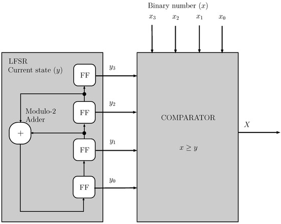 Figure 9. Block diagram of an SNG.
The LFSR module integrates a pseudo-random event which permeates X with randomness properties as outlined in the following paragraph. By convention, 1’s are considered as favorable events and the transformation of x into X takes up to clock cycles (when the maximum length at the output of the LFSR is obtained), with n as the word length of x. In summary, the scalar is encoded by the probability of obtaining a one (favorable event) versus a zero. This is carried out by comparing all the LFSR states () with the same scalar, hence obtaining a binary sequence (bitstream) length.
On the other hand, the decoding is carried out by the summation of favorable events in X divided by ; this yields the probability value .
Since no finite sequence is truly random, the sequence obtained with the LFSR is totally deterministic; the output sequence of the LFSR agrees with the following properties associated with randomness [28]:
- Balance: for every maximum period , the output of the LFSR is balanced and it has approximately 1’s and 0’s;
- Runs: each maximum period has runs of 1’s and runs of 0’s, both of length i with and just one run of 0’s with length and one run of 1’s with length n;
- Span: taking into account all the memory states in the LFSR, it turns out that in a maximum sequence period, all the states appear just one time.
These three properties are the reasons the output sequence of the LFSR is considered a PRBS and is hereinafter referred to as the random sequence (RS).
2.2.2. From PS to WBS
When a mathematical operation or algorithm is implemented with SC logical elements, it can be interpreted as a probability experiment; hence, by counting favorable events, the outcome will be the probabilistic value of such events.
2.3. Stochastic Number Generator
In some SC implementations, the advantage of a small circuit for implementing an algorithm can be dimmed due to SNGs. An SNG requires a certain amount of resources and each input signal or data to the algorithm needs to be transformed by means of an SNG. On the other hand, for a sufficiently large LFSR, it will behave as an ideal random source; otherwise, noise-like random fluctuations appear as errors at the output of the SNG [5]. An alternative version of an SNG known as weighted binary SNG (WBSNG) was introduced in [21], where it was demonstrated that a multiplication free of errors was possible in certain cases by using LFSR. Nevertheless, the WBSNG still requires a considerable amount of resources. In the following, the WBSNG will be reviewed and the proposal of an economical WBSNG (EWBSNG) will be presented.
Remark 3.
Although the WBSNG presented in [21] is is a classic generator, it is still very popular and is used by engineers [2,5].
WBSNG Review
A four-bit version of WBSNG presented in [21] is shown in Figure 10. The main idea behind a WBSNG is to provide an SNG with the capability of assigning to the input binary weights in a descending progression fashion, i.e., , for the PS , supported by the LFSR. Assuming that an LFSR is producing the maximum PS length (), this guarantees that any individual LFSR output bit meets the span property, which implies the balance property too. A balanced sequence has 1’s and 0’s.
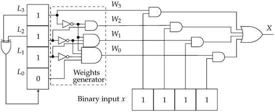
Figure 10.
WBS for [21].
Therefore, counting favorable events in any LFSR output bit position is equivalent to the weight of the Most Significant Bit (MSB) () in a conventional binary number format. This MSB will generate the fundamental sequence to produce the remaining weights. Runs of 1’s and 0’s appear on the same proportions, with a single run of 0’s and a single run of n 1’s; hence, it does not matter what type of run is looked for; both work the same. Here, 0’s runs are considered. Once was defined as a fundamental sequence, it is possible to define weight functions as those shown in Equation (5), which are able to capture the run patterns,
with as an index for the bit sequences produced for the LFSR () and by the weights (), with . Table 1 shows an example of the weight bit streams generated from , when .

Table 1.
SNG output sequence X for x = 0.1111.
3. EWBSNG Proposal
Analyzing the dynamics behavior inside the original WBSNG design, a key pattern is noticed. In Table 1, each time the LFSR has a new state, the defined functions in (5) filter out the binary input by letting pass the most significant bit with value one (MSBO) in the LFSR. Notice that sequences shown in Table 1 do not overlap with each other due to the fact that there is just one bit set to 1 each time, i.e., the MSBO of each LFSR state. Hence, the same MSBO is used like a reference to delimit subsequent runs of 0’s, as can be seen in (5).
Therefore, for a given weight position inside the LFSR, the total number of MSBOs for such a position in a period is equal to the total number of runs of 0’s of length r given before the MSBO. This particular number is . Table 2 shows the above-mentioned facts in an ordered table of states (for ), where it can be noted that the only run of three 0’s () matches with only one MSBO of weight one, satisfying . After the MSBO, the remaining part of the LFSR state consists of do-not-care terms. Hence, the WBSNG shown in Figure 10 searches for all the individual patterns presented in (5), requiring several AND gates to implement them.
Table 2.
Number of MSBOs is equal to the number of runs of 0’s.
A new weight-generating circuit with less hardware can be designed for finding the MSBO in each LFSR state, with the remaining bits as do-not-care terms. For that, the state of the LFSR is complemented, where the MSBO will be zero and propagated through a concatenated structure of AND gates, yielding in that way to the do-not-care bits. Finally, for generating the MSB weight, it is directly connected to the MSB of the LFSR, i.e., , as in the WBSNG. For the remaining weights, XOR gates are used, issuing a logic 1, where a change from 1 to 0 is detected and the remaining weights will issue zeros from the propagated zeros of the concatenated structure of AND gates. The corresponding equations that describe the above-mentioned procedures are as follows:
Finally, the proposed weight-generating circuit for an EWBSNG is shown in Figure 11 for the case of . The rest of the EWBSNG circuit is similar to that shown in Figure 10.
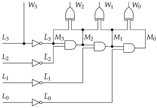
Figure 11.
Weight-generating circuit for .
With respect to Figure 11, the number of occurrences or clock cycles (denoted c. c.) of detected patterns (MSBO in every state of the LFSR) are shown in Table 3, Table 4, Table 5 and Table 6. It can be seen in Table 3 that there are eight occurrences of pattern 1 ([1 ]), where represents do-not-care terms.
Table 3.
Phase 1 of the weight-generating circuit.
Table 4.
Phase 2 of the weight-generating circuit.
Table 5.
Phase 3 of the weight-generating circuit.
Table 6.
Phase 4 of the weight-generating circuit.
In Table 4, the MSBO in each pattern was turned to logic 0. Logic 0 can easily be issued through the do-not-care terms by means of the concatenated AND gates.
The propagated zeros can now be found in Table 5.
In Table 6, it can be noted that a change from logic 1 to 0 is detected from left to right in the state represented by [], yielding to the isolation of the MSBO. This bit represents the weight of its position. This is carried out with XOR gates.
Instead of designing a digital circuit for detecting each pattern as in the original WBSNG; here, a single digital circuit capable of self adjusting for detecting all patterns with less resources was designed. Finally, as can be seen in Figure 10, the last step is the comparison of the weight state [] with the binary input data x, selecting in that way the weights that represent the binary input data in the PS.
Remark 4.
Remark 5.
Since we are not modifying the pseudo-random source (LFSR) and only the comparator inside the SNG is modified without changing its functionality, the effects of the initial seed and the effects of different feedback configurations in the LFSR [28,29] and the correlation study of permuted LFSR outputs as well [17,30] remain the same with respect to the original SNG.
4. Results
The weight-generating circuit is quantified for the one proposed here and is compared with those presented in [20,21]. In order to be able to compare with [20], the final part of the comparator (see Figure 10) was taken into consideration for the one proposed here and the one presented in [21]. Results are shown in Table 7 for any number of bits n.
Table 7.
Logic gates for weight-generating-plus-comparator circuits.
Remark 6.
In the work [20], two new comparator circuits are presented: MPCC-2L and MPCC-ML. According to the authors, the MPCC-ML circuit requires fewer logic gates, but the corresponding logic gates from some flip-flops are not taken into consideration; hence, in this work, the MPCC-2L circuit is taken for comparison purposes.
Figure 12 shows a bar graph of total gates required for the weight-generating circuit here proposed and for that in [20,21]. From Table 7 and Figure 12, it can be appreciated that the proposed circuit has a linear growth of the required logic gates as the number of bits in the word increases, in contrast to the quadratic growth of required logic gates of the proposals in [20,21].
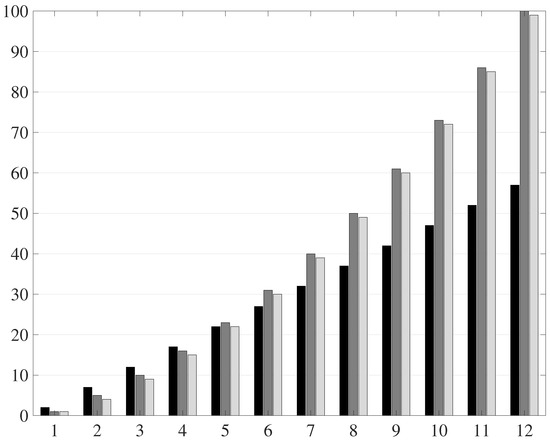
Figure 12.
Bar graph of required logic gates. Proposed circuit (black), [21] (grey), [20] (light grey). Logic gates vs. word length in bits.
5. Conclusions
It is well known that one of most hardware-consuming elements in SC implementation is the SNG; in some cases, the area consumption has been reported to be higher than of the SC circuit itself. From Figure 12, it can be observed that there is a real advantage provided by the proposed circuit with respect to . Nevertheless, common values used in applications are for . In particular, for , the proposed EWBSNG reduces by the number of logic gates with respect to the WBSNG presented in [21]. This is a significant advance that alleviates the problem of large SNG circuits, making SC implementations more attractive.
Author Contributions
Methodology, C.L.-M. and J.R.; Investigation, C.L.-M., J.R., S.O.-C., F.S.-I. and J.L.D.V.; Writing—original draft, C.L.-M. and J.R.; Supervision, J.L.D.V. and F.S.-I.; Funding acquisition, S.O.-C. All authors have read and agreed to the published version of the manuscript.
Funding
This research received no external funding.
Data Availability Statement
No new data were created.
Conflicts of Interest
The authors declare no conflict of interest.
References
- Gaines, B.R. Stochastic computing. In Proceedings of the Spring ACM Joint Computer Conference, Atlantic City, NJ, USA, 18–20 April 1967; pp. 149–156. [Google Scholar]
- Li, H.; Chen, Y. Hybrid Logic Computing of Binary and Stochastic. IEEE Embed. Syst. Lett. 2022, 14, 171–174. [Google Scholar] [CrossRef]
- Kim, J.; Jeong, W.S.; Jeong, Y.; Lee, S.E. Parallel Stochastic Computing Architecture for Computationally Intensive Applications. Electronics 2023, 12, 1749. [Google Scholar] [CrossRef]
- Parhi, M.; Riedel, M.D.; Parhi, K.K. Effect of bit-level correlation in stochastic computing. In Proceedings of the IEEE International Conference on Digital Signal Processing, Singapore, 21–24 July 2015; pp. 463–467. [Google Scholar]
- Alaghi, A.; Hayes, J.P. Survey of Stochastic Computing. ACM Trans. Embed. Comput. Syst. 2013, 12, 1539–9087. [Google Scholar] [CrossRef]
- O’Neill, P.M.; Badhwar, G.D. Single event upsets for Space Shuttle flights of new general purpose computer memory devices. IEEE Trans. Nucl. Sci. 1994, 41, 1755–1764. [Google Scholar] [CrossRef]
- Li, P.; Lilja, D.J.; Qian, W.; Bazargan, K.; Riedel, M.D. Computation on Stochastic Bit Streams Digital Image Processing Case Studies. IEEE Trans. Very Large Scale Integr. (VLSI) Syst. 2014, 22, 449–462. [Google Scholar] [CrossRef]
- Brown, B.D.; Card, H.C. Stochastic neural computation. I. Computational elements. IEEE Trans. Comput. 2001, 50, 891–905. [Google Scholar] [CrossRef]
- Zhang, D.; Li, H. A Stochastic-Based FPGA Controller for an Induction Motor Drive With Integrated Neural Network Algorithms. IEEE Trans. Ind. Electron. 2008, 55, 551–561. [Google Scholar] [CrossRef]
- Ravichandran, H.; Zheng, Y.; Schranghamer, T.F.; Trainor, N.; Redwing, J.M.; Das, S. A Monolithic Stochastic Computing Architecture for Energy Efficient Arithmetic. Adv. Mater. 2023, 35, 2206168. [Google Scholar] [CrossRef] [PubMed]
- Irfan, M.; Yantır, H.E.; Ullah, Z.; Cheung, R.C.C. Comp-TCAM: An Adaptable Composite Ternary Content-Addressable Memory on FPGAs. IEEE Embed. Syst. Lett. 2022, 14, 63–66. [Google Scholar] [CrossRef]
- Alawad, M.; Lin, M. Survey of Stochastic-Based Computation Paradigms. IEEE T Emerg. Topics. Comput. 2019, 7, 98–114. [Google Scholar] [CrossRef]
- Park, J.; Park, S.; Kim, Y.; Park, G.; Park, H.; Lho, D.; Cho, K.; Lee, S.; Kim, D.-H.; Kim, J. Polynomial Model-Based Eye Diagram Estimation Methods for LFSR-Based Bit Streams in PRBS Test and Scrambling. IEEE Trans. Electromagn. Compat. 2019, 61, 1867–1875. [Google Scholar] [CrossRef]
- Lammie, C.; Eshraghian, J.K.; Lu, W.D.; Azghadi, M.R. Memristive Stochastic Computing for Deep Learning Parameter Optimization. IEEE Trans. Circuits II 2021, 68, 1650–1654. [Google Scholar] [CrossRef]
- Liu, Y.; Liu, S.; Wang, Y.; Lombardi, F.; Han, J. A Survey of Stochastic Computing Neural Networks for Machine Learning Applications. IEEE Trans. Neur. Net. Lear. 2021, 32, 2809–2824. [Google Scholar] [CrossRef] [PubMed]
- Lunglmayr, M.; Wiesinger, D.; Haselmayr, W. A Stochastic Computing Architecture for Iterative Estimation. IEEE Trans. Circuits II 2020, 67, 580–584. [Google Scholar] [CrossRef]
- Salehi, S.A. Low-Cost Stochastic Number Generators for Stochastic Computing. IEEE Trans. VLSI Syst. 2020, 28, 992–1001. [Google Scholar] [CrossRef]
- Hu, J.; Li, B.; Ma, C.; Lilja, D.; Koester, S.J. Spin-Hall-Effect-Based Stochastic Number Generator for Parallel Stochastic Computing. IEEE Trans. Electron. Dev. 2019, 66, 3620–3627. [Google Scholar] [CrossRef]
- Liu, S.; Han, J. Energy efficient stochastic computing with Sobol sequences. In Proceedings of the Design, Automation & Test in Europe Conference & Exhibition (DATE), Lausanne, Switzerland, 27–31 March 2017; pp. 650–653. [Google Scholar]
- Collinsworth, C.; Salehi, S.A. Stochastic Number Generators with Minimum Probability Conversion Circuits. In Proceedings of the 2021 IEEE Computer Society Annual Symposium on VLSI (ISVLSI), Tampa, FL, USA, 7–9 July 2021; pp. 49–54. [Google Scholar]
- Gupta, P.K.; Kumaresan, R. Binary multiplication with PN sequences. IEEE Trans. Acoust. Speech. 1988, 36, 603–606. [Google Scholar] [CrossRef]
- Wang, Z.; Ban, T. Design, Implementation and Evaluation of Stochastic FIR Filters Based on FPGA. Circuits Syst. Signal. Process. 2023, 42, 1142–1162. [Google Scholar] [CrossRef]
- Nahar, P.; Khandekar, P.; Deshmukh, M.; Jatana, H.S.; Khambete, U. Survey of Stochastic Number Generators and Optimizing Techniques. In Intelligent Systems and Applications; Kulkarni, A.J., Mirjalili, S., Udgata, S.K., Eds.; Lecture Notes in Electrical Engineering; Springer: Singapore, 2021; Volume 959. [Google Scholar]
- Baker, T.J.; Hayes, J.P. CeMux: Maximizing the Accuracy of Stochastic Mux Adders and an Application to Filter Design. ACM Trans. Des. Autom. Electron. Syst. 2022, 27, 1–26. [Google Scholar] [CrossRef]
- Salehi, S.A. Area-Efficient LFSR-Based Stochastic Number Generators with Minimum Correlation. In IEEE Design & Test; IEEE: Piscataway, NJ, USA, 2023. [Google Scholar] [CrossRef]
- Aygun, S.; Najafi, M.H.; Imani, M.; Gunes, E.O. Agile Simulation of Stochastic Computing Image Processing with Contingency Tables. In IEEE Transactions on Computer—Aided Design of Integrated Circuits and Systems; IEEE: Piscataway, NJ, USA, 2023. [Google Scholar] [CrossRef]
- Parhi, K.K. Analysis of stochastic logic circuits in unipolar, bipolar and hybrid formats. In Proceedings of the IEEE International Symposium on Circuits and Systems, Baltimore, MD, USA, 28–31 May 2017; pp. 1–4. [Google Scholar]
- Golomb, W.S. Shift Register Sequences; Aegean Park Press: Laguna Hills, CA, USA, 1981. [Google Scholar]
- Anderson, J.H.; Hara-Azumi, Y.; Yamashita, S. Effect of LFSR seeding, scrambling and feedback polynomial on stochastic computing accuracy. In Proceedings of the 2016 Design, Automation & Test in Europe Conference & Exhibition (DATE), Dresden, Germany, 14–18 March 2016; pp. 1550–1555. [Google Scholar]
- Salehi, S.A. Low-correlation Low-cost Stochastic Number Generators for Stochastic Computing. In Proceedings of the IEEE Global Conference on Signal and Information Processing (GlobalSIP), Ottawa, ON, Canada, 11–14 November 2019; pp. 1–5. [Google Scholar]
Disclaimer/Publisher’s Note: The statements, opinions and data contained in all publications are solely those of the individual author(s) and contributor(s) and not of MDPI and/or the editor(s). MDPI and/or the editor(s) disclaim responsibility for any injury to people or property resulting from any ideas, methods, instructions or products referred to in the content. |
© 2023 by the authors. Licensee MDPI, Basel, Switzerland. This article is an open access article distributed under the terms and conditions of the Creative Commons Attribution (CC BY) license (https://creativecommons.org/licenses/by/4.0/).