Abstract
This paper proposes a novel control scheme for the buck converter without an inductor current sensor. The architecture of the proposed buck converter is simple and suitable for integration and mass production. It employs an output-voltage-measurement method to determine the switch ON time; therefore, the current sensor is not required. The design specification targets the application with a standard battery power source to generate the low voltages for low-power MCU or ASIC. The load current range aims for several hundred milliamps. The proposed control scheme is analyzed and simulated by SIMPLIS. The control scheme, theoretical analysis, circuit realization, contributions, advantages, and simulation results are presented in this paper. Furthermore, the circuit can be fabricated by a 0.35 μm CMOS process.
1. Introduction
With the rapid development of portable devices, DC-DC converters with fast transient responses and low-power consumption have attracted much attention. Moreover, the power management integrated circuit (PMIC) [1] can provide specific voltages for the system. Therefore, the high-efficiency DC-DC converters play an essential role in electronic systems [2,3,4]. Buck converters now have different control schemes for different applications, such as current mode control (CMC) [5] and voltage mode control (VMC) [6]. In Figure 1, VMC is the simplest control method, which uses the error amplifier to regulate the output. On the contrary, CMC uses fast/slow paths to regulate the output. Therefore, the CMC transient response is better than the VMC one [7].
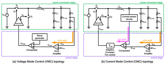
Figure 1.
Control topology of the conventional converter.
Many schemes have been proposed based on CMC, including constant on time (COT) and adaptive on time (AOT). In AOT and COT, AOT has a better transient response than COT [8]. For both COT and AOT, the switching frequency is not fixed, which varies according to the load conditions and output/input voltages. In addition, both COT and AOT have high efficiency in light load. Therefore, the switching frequency is lower in light load, and the switching loss is reduced to improve efficiency. However, this feature will make the electromagnetic interference (EMI) filter hard to design. Generally, the switching converter needs an EMI filter to prevent the coupled impact on the surrounding electrical circuits. Therefore, the constant switching frequency provides a good solution for the EMI issue [9,10].
From the perspective of the transient response, CMC is better than VMC. However, the inductor current sensor is required in CMC, as shown in Figure 1. In the next section, we will investigate various current sensors.
The organizational structure of the paper is as follows: Section 2 is an investigation on various current sensors. Section 3 presents the proposed control scheme and implementation. Section 4 introduces the theoretical analysis. Section 5 shows the SIMPLIS simulation results. Finally, conclusions are given in Section 6.
2. Current Sensor Investigation
Many kinds of current sensors are proposed in [11,12,13,14,15]. If the system requires isolation, the Hall sensor is a candidate. Nevertheless, the Hall-effect current sensors are susceptible to EMI [11]. Therefore, Aiello et al. [12] proposed an EMI-immune contactless current sensor using a split-drain MOS transistor (MagFET). Moreover, a Hall-effect-based current sensor immune to EMI was proposed in [13]. Low-cost isolation current sensors are proposed in [14,15], namely a giant magnetoresistance-effect-based sensor. These contactless current sensors are often used for electrical isolation requirements. Therefore, they may not be suitable for PMIC.
In contrast to the current contactless sensor, sensor-less solutions are more popular and are proposed in [16,17,18,19,20,21,22,23,24,25,26,27]. In Figure 2, the sensing method is straightforward [16,17]. The inductor current information can be obtained through the series resistor, Rdc. The drawback is the additional power consumption in Rdc.
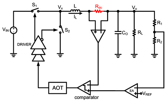
Figure 2.
Control scheme with current-sensing resistor.
In Figure 3, the sensing method uses a low-pass filter set with a parallel inductor, L, [18]. The drawback of this method is that the low-pass filter cannot be integrated into silicon.
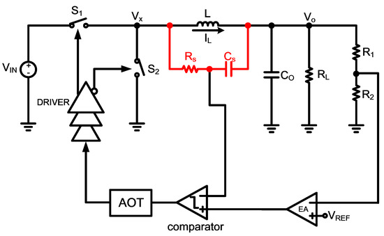
Figure 3.
Control scheme with the low-pass filter.
In Figure 4, the active current-sensing (ACS) circuit is proposed to detect the inductor current [19]. However, the drawback is that the sensing points suffer from significant voltage variation, increasing circuit design complexity.
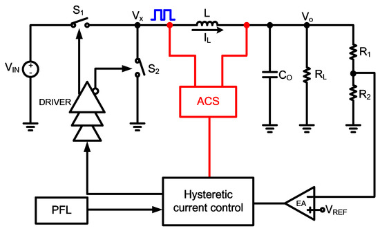
Figure 4.
Control scheme with active current-sensing circuits.
Similarly, in Figure 5, the proposed scheme can improve the transient response [20]. However, the sensing points are still the same as [19].
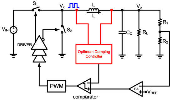
Figure 5.
Control scheme with optimum damping controller.
In Figure 6, the other ACS circuit is employed to sense the voltage, Vx [21]. However, the Vx has a large voltage swing, which increases the input range requirement of the ACS circuit.
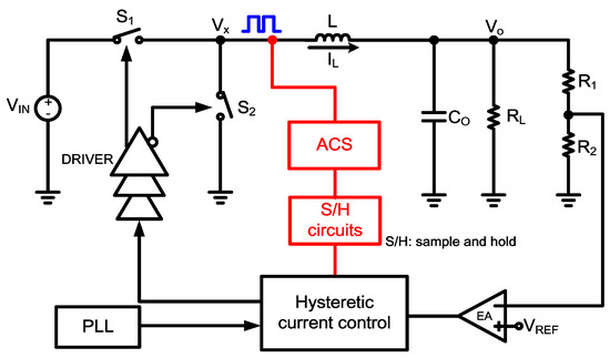
Figure 6.
Control scheme with other ACS circuits.
In Figure 7, the virtual inductor current circuit [21] is proposed to improve the drawback of [19,20,21]. However, this scheme has two drawbacks: (a) the switching frequency is not constant, and (b) the virtual inductor sensor needs the input/output voltages to determine the switch S1 ON time (TON). That means that two sets of voltage-to-current converters are required. Perhaps, the hardware may be further saved. Similarly, [23] proposed the dual loops mechanism buck converter, which uses the input/output voltages to generate TON, instead of the current sensor.
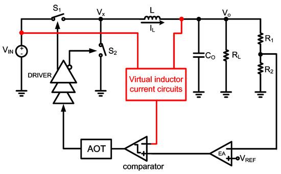
Figure 7.
Control scheme with virtual inductor current circuits.
In Figure 8, the COT buck converter uses an average current-sensing scheme to detect the load current [24]. The drawback is that the circuit that duplicates entire inductor current components increases current consumption as current replication parts increase.
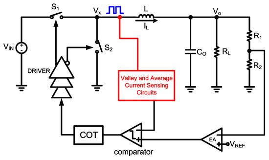
Figure 8.
Control scheme with valley and average current-sensing circuit.
In Figure 9, an AOT-based buck converter with transient-acceleration loops and V-cubic techniques is proposed in [25]. It utilized the techniques of adaptive on-time and V-cubic to stabilize the switching frequency and promote conversion efficiency. Moreover, it is necessary to add a slope-compensation circuit to accelerate the transient response and decrease the transient voltage.
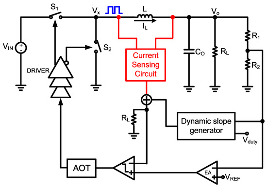
Figure 9.
Control scheme with current sensing circuit.
In Figure 10, a low-noise fast-transient-response continuous-time delta-sigma-modulator (CT-DSM) buck converter is proposed in [26]. The transient-accelerated circuits use a DCR current-sensing circuit and hysteresis-voltage-controlled (HVC) circuit to speed up the transient response. Therefore, the sensing method is similar to [18].
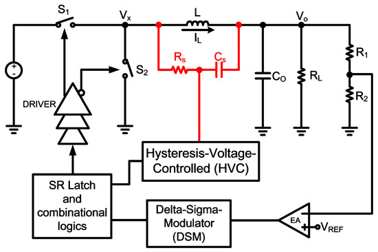
Figure 10.
Control scheme with current-sensing circuit.
A high-efficiency fast transient constant on-time (COT) control DC–DC buck converter with current reused current sensor is proposed in [27]. The current reused current sensor enhances the loop stability and improves the power conversion efficiency at light load.
In this paper, a novel scheme is proposed to simplify circuits further. The contribution and expected outcomes of the designed converter can be listed as (a) simple architecture: it is accessible to implementation, (b) suitable for mass production, (c) high design flexibility: the converter provides more flexible design parameters for various application, (d) the constant switching frequency feature dramatically reduces the difficulty in solving the EMI issue, and (e) good transient response.
3. Proposed Control Scheme, Implementation, and Advantages
3.1. Proposed Control Scheme
Figure 11 shows the proposed control scheme. The function blocks are described as follows:
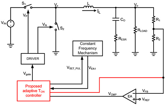
Figure 11.
Control topology of the proposed converter.
- (A)
- Proposed adaptive TON controllerThrough the Vo, the proposed adaptive TON controller module generates a ramp signal and decides TON. The differences from the previous works are listed as follows:
- (a)
- In [22], the TON is decided by the virtual inductor current circuit, which senses the Vin and Vo. Compared with [22], this work eliminates the function of the current sensor. In addition, this work has the feature of the constant switching frequency.
- (b)
- In [23], the TON is decided by the voltage (Vin-Vo). Unlike [23], the TON is decided only by Vo. Moreover, the constant switching frequency mechanism is not the function of Vo. From the methodology perspective, the proposed scheme is different from [22]. This paper proposes another solution for the TON decision. It can further reduce the hardware effort.
- (c)
- In [20], it uses the optimum-damping controller to sense the voltages of the inductor (Figure 5). Compared with [20], this paper dramatically reduces the hardware effort.
- (B)
- Constant frequency mechanism [28]The work of this module mainly makes the switching frequency constant. The module is composed of a frequency detector.
- (C)
- DRIVER:It mainly provides sufficient driving capacity to drive the MOS switches, S1 and S2.
3.2. Implementation and Operating Principle
The implementation of the proposed converter is shown in Figure 12. First, the proposed adaptive TON controller architecture is straightforward and suitable for integration. Second, the circuits do not require a special process to fabricate. Third, the converter uses the constant frequency mechanism module to keep the switching frequency constant instead of PLL. The operation steps of the converter are described as follows (Figure 12):
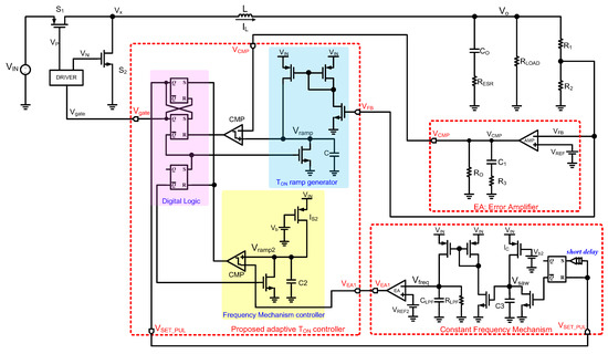
Figure 12.
Implementation of the proposed converter.
- Inductor-charging phase (the switch S1 is ON, and the switch S2 is OFF):The switch S1 ON time is labeled as TON. In Figure 12, the TON is decided by VCMP and Vramp. Once Vramp reaches VCMP, the TON is decided. TON is the function of Vramp. The relationships between TON, Vramp, VFB, and Vo are as follows:
- (a)
- TON is the function of Vramp.
- (b)
- Vramp is the function of VFB.
- (c)
- The relationship between Vo and VFB is a resistor division.
From (a)~(c), we can conclude that TON is the function of Vo. The larger Vo is, the shorter TON is. - Inductor-discharging phase (the switch S1 is OFF, and the switch S2 is ON):The switch S1 OFF time (TOFF) is decided by VEA1 and Vramp2. Once Vramp2 reaches VEA1, the TOFF is decided. The relationship between VEA1 and TOFF is the larger VEA1 and the longer TOFF. In addition, the VEA1 is controlled by the constant frequency mechanism module.
- When the system is stable, the VFB and the Vfreq are almost equal to the VREF and the VREF2, respectively. The VCMP and the VEA1 will eventually converge to their stable voltages. The fundamental waveforms of the converter are drawn in Figure 13.
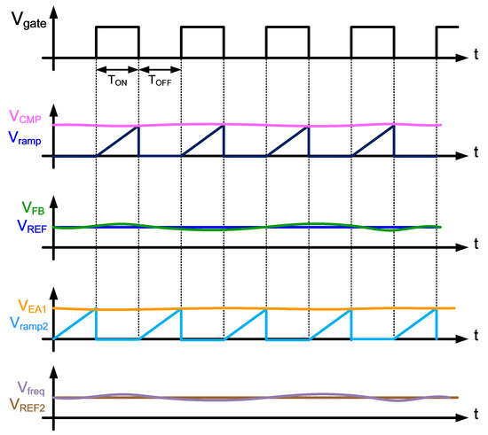 Figure 13. Key waveforms of the proposed converter.
The purpose of different colors in Figure 12 is to clearly show the main function of the proposed adaptive TON controller.
3.3. Proposed Converter Advantages and Disadvantages
3.3.1. Advantages
The proposed converter has four advantages, which are listed below:
- (A)
- The whole circuit does not require a particular process to fabricate.Because the whole circuit does not need special semiconductor devices to implement, there is no need for a specific process in fabrication.
- (B)
- There is no special layout/matching issue in the circuit.Layout is an important step in fabrication. Fortunately, there is no special matching issue in the proposed circuits.
- (C)
- The whole circuit is robust.Each crucial parameter has considered its design margin and the process variation.
- (D)
- The feature of constant switching frequency dramatically reduces the difficulty of solving the EMI issue.The variable switching frequency makes the electromagnetic interference (EMI) filter hard to design.
3.3.2. Disadvantages
The proposed converter has four disadvantages, which are listed below:
- (A)
- The proposed converter has a slight switching frequency drift. The switching frequency is approximately 1.01–1.05 MHz. The variation is about 3.5%. However, this slight variation is acceptable for solving the EMI issue.
- (B)
- The regulation capability is poor at the input voltage of 3.6 V and the output voltage of 1.0 V. The maximum ripple voltage of the output is about 11.2 mV. The performance of the boundary conditions is barely acceptable.
4. Theoretical Analysis
4.1. Mathematical Model
In this section, the mathematical model of the buck converter will be illustrated. It can assist in confirming stability. Many studies [29,30,31,32] about modeling ways are proposed. Chou et al. [22,28] presents the design procedure in detail. The mathematical model is built through Reference [32] in this paper. In Figure 14, the open-loop transfer function of the converter can be expressed as Equation (1). Equation (2) represents the GP(s) of the buck converter. A(s) represents the error amplifier composed of the transconductance, gm, and the compensation network.
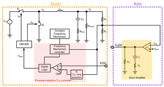
Figure 14.
Block diagram of the overall transfer function.
In Figure 14, the Ki, RO, R3, and C1 are the key parameters, and the relations are shown in Equations (1)–(3). The purpose of different colors in Figure 14 is to clearly find the function blocks in Figure 12. According to [29,30], in Equation (4), we locate the zero, wz, at the output pole of the buck converter. The pole, wp, is a free design parameter. Therefore, we choose a suitable wp to make the system stable. The design procedure is described in [22,28] and is verified by MathCAD and SIMPLIS.
where is the gain of the TON ramp generator, , , .
4.2. Design Parameters and Components Selection
By references [22,28], we can use MathCAD to calculate the design parameters of the converter. Compared with previous works, the external components and load conditions have not changed. The design parameters of this work are listed in Table 1.

Table 1.
Design parameters and component value.
5. Simulation Results
5.1. SIMPLIS Schematic
The SIMPLIS schematic of the proposed converter is built and shown in Figure 15.
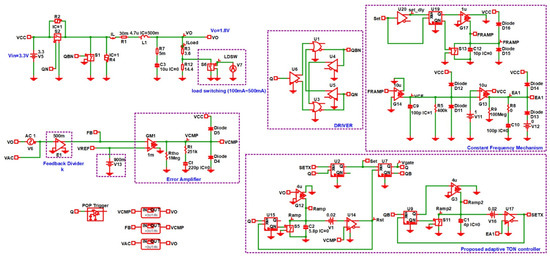
Figure 15.
Schematic of the proposed converter.
5.2. Transient Performance
The transient response at the load transition is shown in Figure 16 under the test conditions of 0.1–0.5 A load current and 3.3 V/1.8 V input/output voltage. The recovery time means that the output voltage recovers to 1% of 1.8 V at the load change.
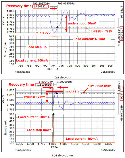
Figure 16.
Recovery times for load current transition between 100–500 mA.
In Figure 16, the step-up and step-down recovery times are 1.8 μs and 1.5 μs, respectively. From the results, the recovery time is less than 2 μs. In addition, Figure 16 shows that the overshoot/undershoot voltages are 21 mV/30 mV.
The converter specifies that Vin is 3.0–3.6 V and Vo is 1.0–2.5 V. Figure 17 illustrates that the maximum ripple voltage is 11.2 mV at the input voltage of 3.6 V and the output voltage of 1.0 V.
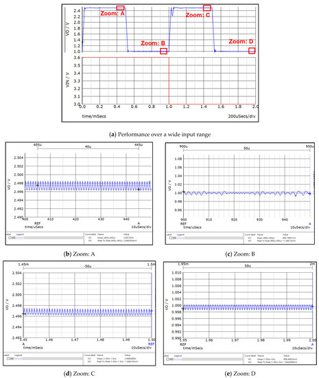
Figure 17.
Simulation results under different input/output voltages.
5.3. Load Regulation
The load regulation follows Equation (5). This specification indicates the output regulation capability when the load changes. The load regulation should be as small as possible for a good design. In this paper, the simulation conditions are the input/output voltages are 3.3 V/1.8 V, and the load current varies from 0.5 A to 0.1 A. As shown in Figure 18, the load regulation is nearly 0% by Equation (5).
where is the voltage at the 0.5 A load current, and is the voltage at the 0.1 A load current.
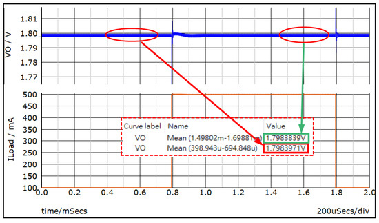
Figure 18.
Load regulation.
5.4. Line Regulation
The line regulation follows Equation (6). This specification indicates the output regulation capability when the supply voltage changes. The line regulation should be as small as possible for a good design. In this paper, the supply voltage varies from 3.0 V to 3.6 V. Therefore, by Equation (6), the simulation value is close to 0.
where ΔVin is the variation of the input voltage, and ΔVo is the variation of the output voltage.
5.5. Switching Frequency Regulation
Figure 19 illustrates the switching frequency of the different output voltages. The results show that: (a) At the output voltage of 1.0–2.5 V, the switching frequency is approximately 1.011–1.046 MHz. (b) The switching frequency is about 1.02 MHz at an output voltage of 1.8 V. (c) The frequency variation is roughly 3.5%. It has a slight frequency drift that results from the EA1 of the constant frequency mechanism module in Figure 12. The EA1 cannot regulate well the Vfreq to the VREF2 at the lower output voltage. The lower Vo leads to the lower Vfreq, slightly weakening the regulation ability.
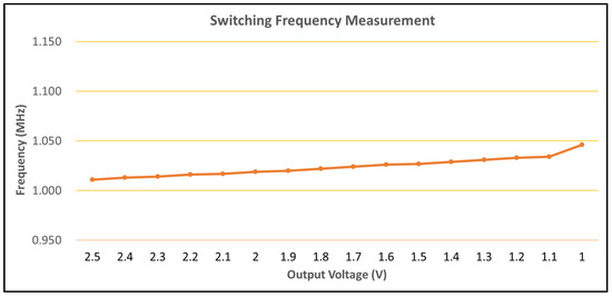
Figure 19.
Switching frequency results.
5.6. Performance List
The performance of the novel buck converter is summarized in Table 2. From 100 mA to 500 mA load current, the recovery time is less than 2 μs. The converter has a good performance under the supply voltage of 3.0–3.6 V and the output voltage of 1.8 V. Finally, the performance comparisons with reported converters are listed in Table 3. Table 3 shows that the performance is still different even in the same control scheme. The reason comes from the different switching methods and circuit schemes. Generally, the transient response is greatly affected by external components, such as the load capacitor, inductor, and load. Therefore, we need to use the same load conditions for fair comparisons.
Table 2.
Performance Summary.
Table 3.
Performance Comparisons with Reported Converters.
In Table 3, we compare this work to the others, make some discussions, and list as follows:
- (A)
- Compared with [33], the proposed scheme can provide better recovery time.
- (B)
- In [24,33], the output voltage is a fixed value. However, this work can provide greater flexibility for the output.
- (C)
- Compared with [23], although the performance on recovery time and switching frequency variation are slightly worse, the control scheme is simple and easy to implement, and these performance differences are not particularly obvious in application.
- (D)
- Compared with [22], this work can provide an approximately constant switching frequency.
- (E)
- Compared with [28], the most significant improvement is that the current sensor is not required. In addition, the proposed converter is straightforward.
- (F)
- Compared with [26], the switching frequency of this work is lower, and the switching loss is reduced. The [26] uses the DCR current-sensing and hysteresis-voltage-controlled (HVC) circuits to speed up the transient response. However, the circuits are more complicated than this work.
- (G)
- From Table 3, this work has a better transient response than [19,24,25,26,27], probably because this work is the simulation result.
- (H)
- Compared with [19], this work provides a simple scheme to keep the switching frequency constant. The [19] uses the PLL function block to achieve the switching frequency constant.
- (I)
- Compared with [25], the proposed scheme provides the output of 1.0–2.5 V. Additionally, [25] can provide a low output voltage of 0.4 V, suitable for low supply power systems. Moreover, [25] can adopt a lower inductor than this work.
- (J)
- In [24,27], the converters all use the COT control scheme. There is no feature of constant switching frequency in [24]. The [27] uses a current reused current sensor to enhance the loop stability. The [24] experiences a large overshoot/undershoot.
- (K)
- In [35], a current-mode hysteretic buck converter is presented in which the inductor current is sensed by a resistor-capacitor (RC) network. The sensing method is similar to [18]. (Figure 3) From Table 3, the undershoot/overshoot of the converter [34] is larger than 50 mV. In [35], the transient response of the converter is relatively poor.
- (L)
- Compared with [20,34,35,36,37], the proposed converter can provide a good transient response.
6. Conclusions
This paper proposes a novel buck converter with no current sensor. The performance of this converter is not inferior to that of CMC. The converter uses sensing of the Vo to generate the TON instead of the current sensor. There are four advantages to this converter. First, the whole circuit does not require a special process to fabricate. Second, there is no special layout-matching issue in the circuit. Third, the whole circuit is robust. Each crucial parameter has considered its design margin and process variation. Forth, the feature of constant switching frequency dramatically reduces the difficulty of solving the EMI issue. The design spec of the buck converter prototype is an output voltage of 1.0–2.5 V at the in-put voltage of 3.0–3.6 V. The driving capacity of the load current ranges from 100 mA to 500 mA. The scheme is verified by SIMPLIS. The simulation results show that the switching frequency variation is less than 3.5% at the output voltage of 1.0–2.5 V. The recovery time is less than 2 μs during the load change. The proposed converter can be implemented further with a 0.35 μm CMOS process.
Author Contributions
Conceptualization, H.-H.C.; Data curation, W.-H.L.; Methodology, H.-H.C.; Validation, H.-H.C.; Writing—original draft, H.-H.C.; Writing—review & editing, H.-H.C. and S.-F.W. All authors have read and agreed to the published version of the manuscript.
Funding
This research was funded by Ministry of Science and Technology, Taiwan, under Grants MOST 110-2222-E-346-001.
Conflicts of Interest
The authors declare no conflict of interest.
Abbreviations
| TON | switch S1 ON time |
| TOFF | switch S1 OFF time, (switch S1 is shown in Figure 11) |
References
- Redl, R.; Sun, J. Ripple-based control of switching regulators—An overview. IEEE Trans. Power Electron. 2009, 24, 2669–2680. [Google Scholar] [CrossRef]
- Chen, W.-C. Reduction of equivalent series inductor effect in delay-ripple reshaped constant on-time control for buck converter with multilayer ceramic capacitors. IEEE Trans. Power Electron. 2013, 28, 2366–2376. [Google Scholar] [CrossRef]
- Chen, J.J.; Lu, M.-X.; Wu, T.-H.; Hwang, Y.S. Sub-1-V fast response hysteresis-controlled CMOS buck converter using adaptive ramp techniques. IEEE Trans. Very Large Scale Syst. 2013, 21, 1608–1618. [Google Scholar] [CrossRef]
- Chen, J.J.; Hwang, Y.S.; Chen, J.H.; Ku, Y.T.; Yu, C.C. A New Fast-Response Current-Mode Buck Converter with Improved I2-Controlled Techniques. IEEE Trans. Very Large Scale Integr. Syst. 2018, 26, 903–911. [Google Scholar] [CrossRef]
- Chen, W.W.; Chen, J.F.; Liang, T.J.; Wei, L.C.; Ting, W.Y. Designing a Dynamic Ramp with an Invariant Inductor in Current-Mode Control for an On-Chip Buck Converter. IEEE Trans. Power Electron. 2014, 29, 750–758. [Google Scholar] [CrossRef]
- Saini, D.K.; Reatti, A.; Kazimierczuk, M.K. Average Current-Mode Control of Buck DC-DC Converter with Reduced Control Voltage Ripple. In Proceedings of the 42nd Annual Conference of the IEEE Industrial Electronics Society, IECON, Florence, Italy, 24–27 October 2016. [Google Scholar] [CrossRef][Green Version]
- Liu, J.M.; Wang, P.Y.; Kuo, T.H. A current-mode DC–DC buck converter with efficiency-optimized frequency control and reconfigurable compensation. IEEE Trans. Power Electron. 2012, 27, 3085–3094. [Google Scholar] [CrossRef]
- Li, Y.; Chen, C.; Tsai, C. A Constant On-Time Buck Converter with Analog Time-Optimized On-Time Control. IEEE Trans. Power Electron. 2020, 35, 3754–3765. [Google Scholar] [CrossRef]
- Zheng, Y.; Chen, H.; Leung, K.N. A fast-response pseudo-PWM buck converter with PLL-based hysteresis control. IEEE Trans. Very Large Scale Integr. Syst. 2012, 20, 1167–1174. [Google Scholar] [CrossRef]
- Yuan, B.; Liu, M.; Ng, W.T.; Lai, X. A Fast-Response RBAOT-Controlled Buck Converter with Pseudofixed Switching Frequency and Enhanced Output Accuracy. IEEE J. Emerg. Sel. Top. Power Electron. 2021, 9, 79–88. [Google Scholar] [CrossRef]
- Aiello, O. Hall-Effect Current Sensors Susceptibility to EMI: Experimental Study. Electronics 2019, 8, 1310. [Google Scholar] [CrossRef]
- Aiello, O.; Fiori, F. A New MagFET-Based Integrated Current Sensor Highly Immune to EMI. Microelectron. Reliab. 2013, 53, 573–581. [Google Scholar] [CrossRef]
- Dalessandro, L.; Karrer, N.; Kolar, J.W. High-Performance Planar Isolated Current Sensor for Power Electronics Applications. IEEE Trans. Power Electron. 2007, 22, 1682–1692. [Google Scholar] [CrossRef]
- Ouyang, Y.; He, J.; Hu, J.; Wang, S.X. A current sensor based on the giant magnetoresistance effect: Design and potential smart grid applications. Sensors 2012, 12, 15520–15541. [Google Scholar] [CrossRef] [PubMed]
- Jantaratana, P.; Sirisathitkul, C. Low-cost sensors based on the GMI effect in recycled transformer cores. Sensors 2008, 8, 1575–1584. [Google Scholar] [CrossRef] [PubMed]
- Sheehan, R. Understanding and Applying Current-Mode Control Theory. Texas Instruments Technical Document Application Reports. Literature Number: SNVA555. 2007. Available online: https://www.ti.com/lit/pdf/snva555 (accessed on 31 August 2021).
- Song, C. Accuracy Analysis of Constant-On Current-Mode DC-DC Converters for Powering Microprocessors. In Proceedings of the 2009 Twenty-Fourth Annual IEEE Applied Power Electronics Conference and Exposition, Washington, DC, USA, 21 March 2009. [Google Scholar] [CrossRef]
- Zhen, S.; Zeng, P.; Chen, J.; Zhou, W.; Wang, J.; Luo, P.; Zhang, B. Transient Response Improvement of DC-DC Converter by Current Mode Variable on Time Control. In Proceedings of the 2018 IEEE 61st International Midwest Symposium on Circuits and Systems (MWSCAS), Windsor, ON, Canada, 5–8 August 2018. [Google Scholar] [CrossRef]
- Chen, J.J.; Hwang, Y.S.; Ku, Y.T.; Li, Y.H.; Chen, J.A. A Current-Mode-Hysteretic Buck Converter with Constant-Frequency-Controlled and New Active-Current-Sensing Techniques. IEEE Trans. Power Electron. 2021, 36, 3126–3134. [Google Scholar] [CrossRef]
- Hwang, Y.S.; Chen, J.J.; Ku, Y.T.; Yang, J.Y. An Improved Optimum-Damping Current-Mode Buck Converter with Fast-Transient Response and Small-Transient Voltage Using New Current Sensing Circuits. IEEE Trans. Ind. Electron. 2021, 68, 9505–9514. [Google Scholar] [CrossRef]
- Chen, J.-J. An Active Current-Sensing Constant-Frequency HCC Buck Converter using Phase-Frequency-Locked Techniques. IEEE Trans. Ultrason. Ferroelectr. Freq. Control 2008, 55, 761–769. [Google Scholar] [CrossRef]
- Chou, H.-H.; Chen, H.-L.; Fan, Y.-H.; Wang, S.-F. Adaptive On-Time Control Buck Converter with a Novel Virtual Inductor Current Circuit. Electronics 2021, 10, 2143. [Google Scholar] [CrossRef]
- Chou, H.-H.; Luo, W.-H.; Chen, H.-L.; Wang, S.-F. A Novel Buck Converter with Dual Loops Control Mechanism. Electronics 2022, 11, 1256. [Google Scholar] [CrossRef]
- Jeon, I.; Min, K.; Park, J.; Roh, J.; Moon, D.; Kim, H. A Constant On-Time Buck Converter with Fully Integrated Average Current Sensing Scheme. In Proceedings of the 2021 18th International SoC Conference (ISOCC 2021), Jeju, Korea, 6–9 October 2021. [Google Scholar] [CrossRef]
- Chen, J.-J.; Hwang, Y.-S.; Jiang, W.-M.; Lai, C.-H.; Ku, J. A New Improved Ultra-Fast-Response Low-Transient-Voltage Buck Converter with Transient-Acceleration Loops and V-Cubic Techniques. IEEE Access 2022, 10, 3601–3607. [Google Scholar] [CrossRef]
- Chen, J.-J.; Hwang, Y.-S.; Liu, H., Jr.; Lai, C.-H.; Ku, Y. A Low-Noise Fast-Transient-Response Buck Converter Suitable for Sensor Networks with New Transient-Accelerated-Circuits. IEEE Sens. J. 2022, 22, 2868–2876. [Google Scholar] [CrossRef]
- ul Ain, Q.; Khan, D.; Jang, B.G.; Basim, M.; Shehzad, K.; Asif, M. A High-Efficiency Fast Transient COT Control DC–DC Buck Converter with Current Reused Current Sensor. IEEE Trans. Power Electron. 2021, 36, 9521–9535. [Google Scholar] [CrossRef]
- Chou, H.-H.; Chen, H.-L. A Novel Buck Converter with Constant Frequency Controlled Technique. Energies 2021, 14, 5911. [Google Scholar] [CrossRef]
- Li, J.; Lee, F.C. New modeling approach and equivalent circuit representation for current-mode control. IEEE Trans. Power Electron. 2010, 25, 1218–1230. [Google Scholar] [CrossRef]
- Enrique, J.M.; Barragán, A.J.; Durán, E.; Andújar, J.M.; Gómez, J.M.E.; Piña, A.J.B.; Aranda, E.D.; Márquez, J.M.A. Theoretical Assessment of DC/DC Power Converters’ Basic Topologies. A Common Static Model. Appl. Sci. 2017, 8, 19. [Google Scholar] [CrossRef]
- Suntio, T. Dynamic Modeling and Analysis of PCM-Controlled DCM-Operating Buck Converters—A Reexamination. Energies 2018, 11, 1267. [Google Scholar] [CrossRef]
- Ridley, R.B. An Accurate and Practical Small-Signal Model for Current-Mode Control. Available online: www.ridleyengineering.com (accessed on 24 July 2021).
- Jiang, C.R.; Chai, C.C.; Han, C.X.; Yang, Y.T. A high performance adaptive on-time controlled valley-current-mode DCDC buck converter. J. Semicond. 2020, 41, 062406. [Google Scholar] [CrossRef]
- Jeong, M.-G.; Kang, J.-G.; Park, J.; Yoo, C. A Current-Mode Hysteretic Buck Converter with Multiple-Reset RC-Based Inductor Current Sensor. IEEE Trans. Ind. Electron. 2019, 66, 8445–8453. [Google Scholar] [CrossRef]
- Nashed, M.; Fayed, A.A. Current-mode hysteretic buck converter with spur-free control for variable switching noise mitigation. IEEE Trans. Power Electron 2018, 33, 650–664. [Google Scholar] [CrossRef]
- Jung, D.-H.; Kim, K.; Joo, S.; Jung, S.-O. 0.293-mm2 fast transient response hysteretic quasi-V2 DC-DC converter with area-efficient timedomain-based controller in 0.35-μm CMOS. IEEE J. Solid-State Circuits 2018, 53, 1844–1855. [Google Scholar] [CrossRef]
- Chen, J.J.; Hwang, Y.S.; Lin, J.Y.; Ku, Y. A dead-beat-controlled fast-transient-response buck converter with active pseudo-current-sensing techniques. IEEE Trans. Very Large Scale Integr. Syst. 2019, 27, 1751–1759. [Google Scholar] [CrossRef]
Publisher’s Note: MDPI stays neutral with regard to jurisdictional claims in published maps and institutional affiliations. |
© 2022 by the authors. Licensee MDPI, Basel, Switzerland. This article is an open access article distributed under the terms and conditions of the Creative Commons Attribution (CC BY) license (https://creativecommons.org/licenses/by/4.0/).