Abstract
In-memory computing (IMC) aims to solve the performance gap between CPU and memories introduced by the memory wall. However, it does not address the energy wall problem caused by data transfer over memory hierarchies. This paper proposes the data-locality management unit (DMU) to efficiently transfer data from a DRAM memory to a computational SRAM (C-SRAM) memory allowing IMC operations. The DMU is tightly coupled within the C-SRAM and allows one to align the data structure in order to perform effective in-memory computation. We propose a dedicated instruction set within the DMU to issue data transfers. The performance evaluation of a system integrating C-SRAM within the DMU compared to a reference scalar system architecture shows an increase from to in speed-up and from to in energy reduction, versus a system integrating C-SRAM without any transfer mechanism compared to a reference scalar system architecture.
1. Introduction
Von Neumann architectures are limited by the performance bottleneck characterized by the “memory wall”, i.e., the performance limitation of memory units compared to CPU, and the “energy wall”, i.e., the gap between the energies consumed for computation and data transfers between different system components.
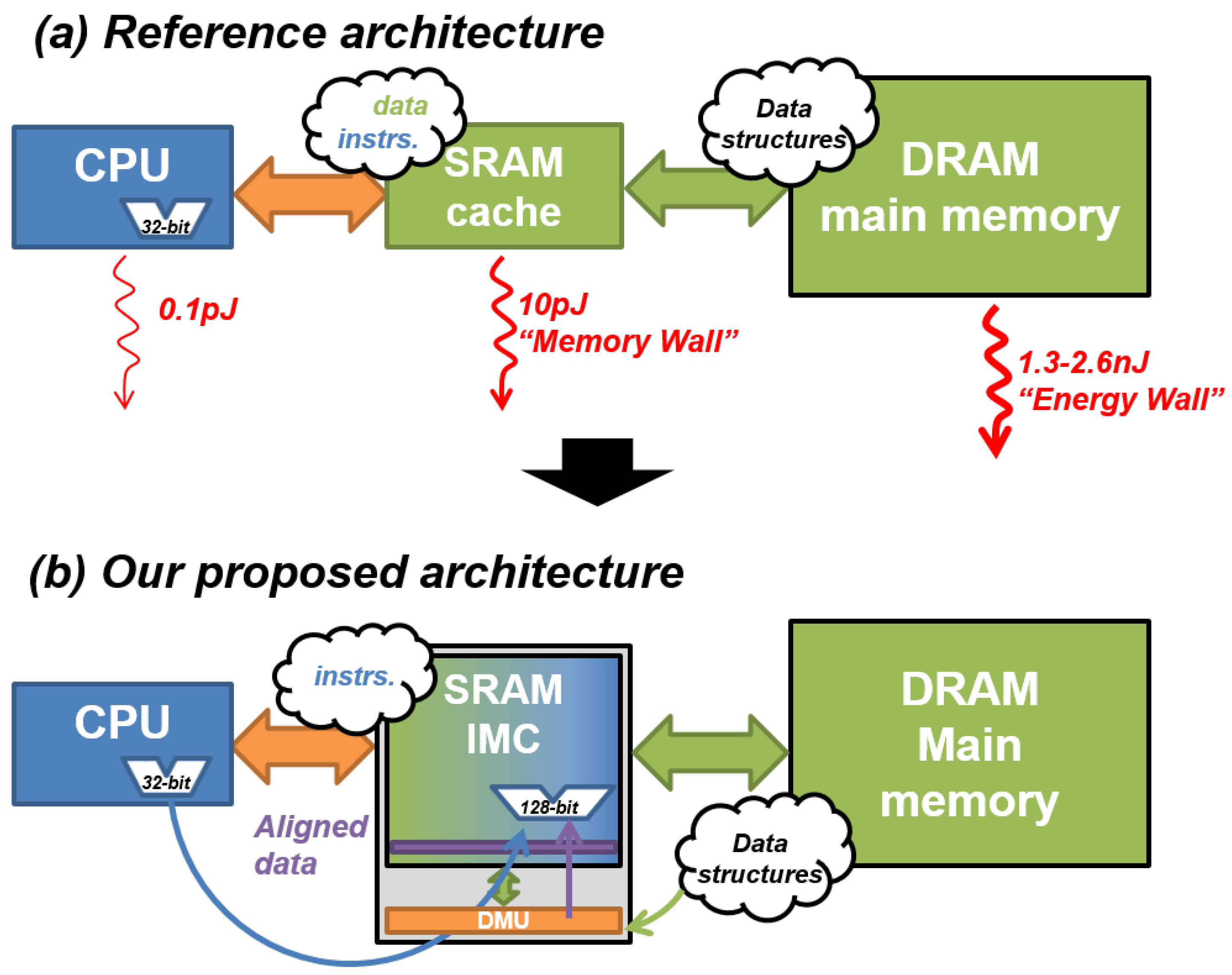
Figure 1a exposes the energy discrepancy between each component of a standard von Neumann architecture. We note that the energy increases by between the CPU and the cache memory, and by between the CPU and the DRAM memory [1]. In-memory computing (IMC) is a solution to implement non-von Neumann architectures and mitigate the memory wall by moving computation directly into memory units [2]. It allows the reduction of data transfers and thus energy consumption. However, the efficiency of IMC depends on the proper arrangement of data structures. Indeed, to be correctly computed in the memory, data should be arranged to respect a precise order (e.g., aligned in memory rows) imposed by IMC hardware design constraints.
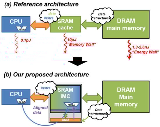
Figure 1.
(a) Performance bottlenecks of von Neumann architecture; energy costs are based on [1]. (b) Proposed architecture with IMC to mitigate the “memory wall” and a “DMU” block to mitigate the “energy wall” between IMC and low-latency memory.
While various state-of-the-art works propose IMC solutions, very few take into account their integration to complete computer systems while describing efficient methods to transfer data from IMC to high-latency memories or peripherals. This lack of consideration can be explained by the majority of IMC architectures being currently specialized for a few use cases, i.e., AI and big data, which limits their efficiency for general-purpose computing. We propose a data-locality management unit (DMU), a transfer block presented in Figure 1b, coupled to an SRAM-based IMC unit to generate efficient data transfer and reorganization through a dedicated instruction set. As IMC architecture, we consider the computational SRAM (C-SRAM), an SRAM-based bit-parallel IMC architecture detailed in [2,3,4], and able to perform logical and arithmetical operations in-parallel thanks to an arithmetic and logic unit (ALU) in its periphery. We integrate it within a CPU and a DRAM as main memory.
The system evaluation of C-SRAM and DMU on three applications—frame differencing, Sobel filter and matrix multiplication—versus a system integrating C-SRAM without a dedicated transfer mechanism shows an increase from to in speed-up and from to in energy reduction, according to a baseline scalar architecture.
2. Related Work
2.1. In-Memory Computing (IMC)
IMC architectures of the state-of-the-art can be differentiated by their technology and programming model [5]. Volatile memory-based IMC architectures include DRAM and SRAM technologies. DRAM-based IMC architectures propose to enhance DRAM memories with bulk-bitwise computation operators. These solutions offer cost and area efficiency and large parallelism, although their arithmetic support is limited to logical or specialized operators [6,7]. SRAM-based IMC architectures are less scalable than DRAM-based solutions in terms of design, but they implement more elaborated computation operators, either through strict IMC using bit-lines and sense amplifiers, or through near-memory computing by using an arithmetic logic unit (ALU) in the periphery of the bit-cell array [3,8,9]. Other approaches using emerging technologies such as MRAM or Re-RAM [10,11] have been explored. They present interesting opportunities in terms of access latency and nonvolatile capability, but have drawbacks in terms of cycle-to-cycle variability and analog-to-digital conversion of input data.
Despite all these technological differences, a common challenge regarding system integration is the specific memory management required to properly map data to be able to perform effective computations. A study of the literature presents three main mapping strategies of existing IMC architectures. First, bit-parallel mapping requires each operand of a given operation to be aligned on the same bit-cells to be computed, which induces the logical memory alignment of data [3,6]. Then, in bit-serial data mapping, operands are aligned on the same rows, and all bits of a given operand are aligned on the same bit-cell [8]. This requires data to be physically transposed in the array to be effectively computed. Third, crossbar mapping is a 2D mapping scheme used to perform computation in the form of convolutions between analog data driven through different word-lines and data along each bit-line [11]. Bit-serial and crossbar mapping schemes show advantages in terms of computation capabilities, but are difficult to integrate due to their data management constraints (data transposing for bit-serial and digital-to-analog conversion and rearrangement for crossbar) which conflict with the inherent bit-parallel nature of modern computer systems.
In this paper, we focus on an SRAM-based bit-parallel architecture, which shows a better compromise between computation capability, system integration and data compatibility [2,3,4].
2.2. Data Management Solutions for IMC
In this subsection, we focus on data management solutions devised by previous works for IMC architectures. First, IMC architectures based on emerging technologies evaluate their solutions while not considering the cost of external data transfers with high-latency memories or peripherals, as their architectures are not yet mature for system integration. We only retain two state-of-the-art solutions of data management when focusing on conventional technologies, e.g., DRAM and SRAM-based.
“PIM-enabled instructions” [12] (PEI) establishes the specifications for a generic IMC architecture while also defining its integration to the memory hierarchy. PEI computation units (PCU) are integrated within a hybrid memory cube, each managing a DRAM module to perform NMC on the main memory while a local PCU is coupled to the host CPU to perform NMC at the cache-level, e.g., on SRAM. While the paper proposes hardware and software mechanisms to ensure data coherency and locality management, the complexity of this solution makes this architecture difficult to implement and program. Moreover, the cost of data movements for PCUs computing on DRAM means that data management needs to be statically scheduled to reduce dynamic rearrangement as often as possible. Finally, PEI does not define specialized instructions for memory accesses, limiting the charge of data management to the host CPU and extending it to DRAM memory.
The duality cache [8] is designed to be implemented in the last-level cache (LLC). Its data management mechanism is based on the cache controller of the LLC to transfer data to different data banks. Other mechanisms such as the transpose memory unit (TMU) are implemented to transpose data from bit-parallel-in-DRAM to bit-serial-in-IMC. While the hardware and software environment of the duality cache make for an effective data management mechanism for its target applications (GPU kernels, especially AI), it is not explicitly programmable and it is constraining for developers. This limitation implies the static allocation and management of data before computation, and according to the hardware mechanisms of the duality cache.
The transfer mechanism we describe in this paper proposes a dedicated instruction set, integrated as an extension of the IMC ISA to offer explicit management on dynamically allocated data to developers. Compared to previous solutions, our interest is compatibility with general-purpose computing.
3. DMU Specification
3.1. Overview
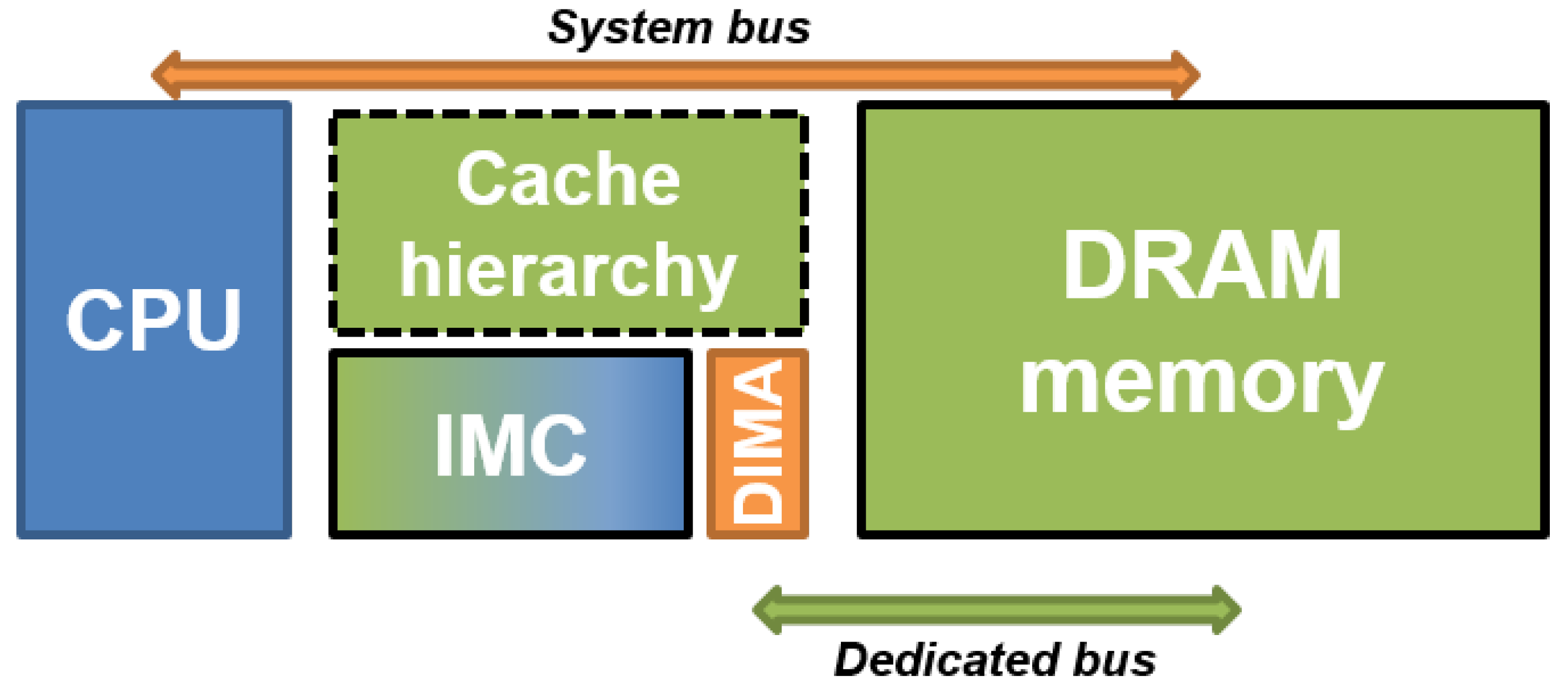
In this section, we present a DMU, a memory controller architecture to provide memory access instructions to IMC to efficiently transfer and reorganize data before computation. We implement in the DMU the control of source and destination offsets to enable fine-grain data reorganization in IMC as well as DRAM memory to address alignment constraints necessary for certain applications, and the implementation of two different operating modes makes online data padding available. Finally, the DMU implements a dedicated instruction set to program data transfers in a single clock cycle, compared to classical DMA solutions. This instruction set is implemented as a subset of the C-SRAM instruction set architecture. The DMU controller is proposed to be tightly coupled in the periphery of the IMC unit, as shown in Figure 2. This means that there is a direct interface between the DMU and IMC without going through the system bus, which is one of the main difference compared to existing DMA controllers.
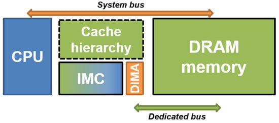
Figure 2.
The integration of DMU to IMC offers an instruction set for efficient data transfers as well as a dedicated transfer bus with the main memory.
3.2. Instruction Set Architecture
Table 1 shows the proposed instructions defined for the DMU. All instructions are nonblocking for the host architecture, and a BLOCKING_WAIT instruction is implemented to ensure synchronization between it and the C-SRAM.

Table 1.
Summary of DMU instructions.
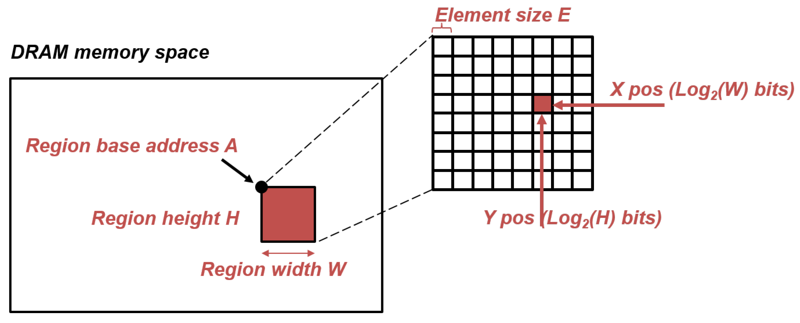
SET_SRC_DRAM_REGION and SET_DST_DRAM_REGION take as parameters 2D regions in DRAM memory space, characterized by: their base address A and their width and height, respectively, W and H. The number of bits required for A is architecture-dependent while the numbers of bits required to encode H and W are implementation-dependent. By defining in advance the source and destination data structures in DRAM, READ_TRANSFER and WRITE_TRANSFER instructions only require, respectively, the source and destination positions (X, Y) in the target region, which can be encoded in and bits. This indirect addressing effectively reduces the number of bits required for both instructions, which are the most frequently called instructions of the instruction set. Figure 3 illustrates this mechanism from the developer’s point of view.

Figure 3.
Representation of a 2D region in the DRAM memory space, defined by SET_DRAM_REGION, and a single element in said region. This decomposition allows reducing the number of bits required in transfer instructions for DRAM address.
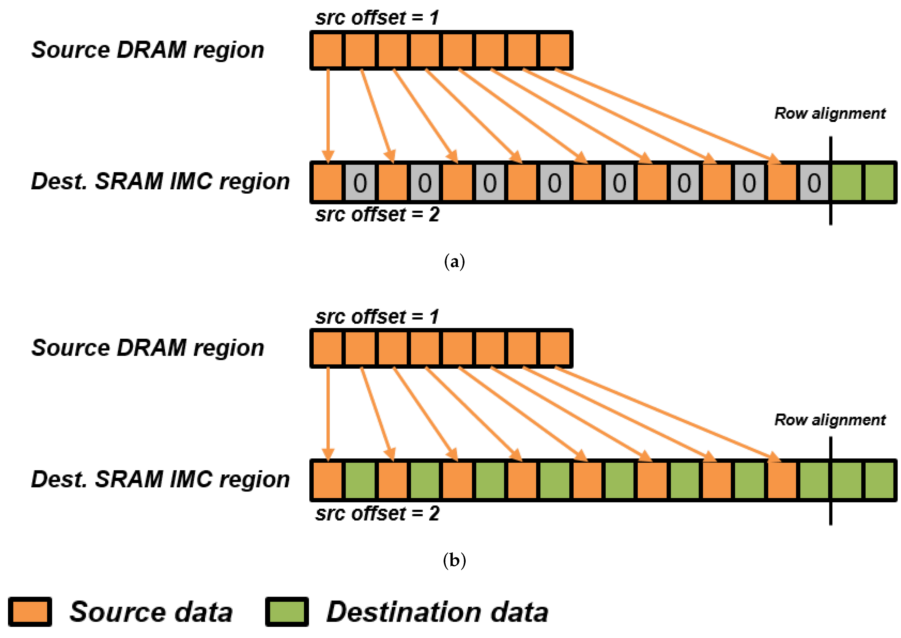
READ_TRANSFER, WRITE_TRANSFER and COPY can operate to transfer data and perform online reorganization. For example, the parameterizing of source and destination offsets allow the data to be padded upon arrival in the C-SRAM. To cover most use-cases induced with the configuration of the destination offset, we implement in the DMU two operating modes through the transfer_start register, illustrated in Figure 4. A zero-padding mode fills the blanks in between destination data with zeros to perform unsigned byte extension, while an overwriting mode preserves the data present in the destination C-SRAM row and updates only relevant bytes. The former is destructive but enables online byte extension to perform higher-precision arithmetic for workloads such as image processing or machine learning, while the latter is more suitable for nondestructive data movements. Since most iterative codes such as convolutions induce strong data redundancy, COPY can be used to duplicate data and mitigate accesses with the DRAM for better energy efficiency.
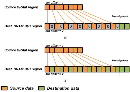
Figure 4.
DMU operating modes and their impact on destination memory, here an SRAM IMC memory. (a) Zero-padding mode. (b) Overwriting mode.
Algorithm 1 describes the side effects generated by the READ_TRANSFER instruction, according to its parameters and the offset mechanism described in Figure 4.
| Algorithm 1:READ_TRANSFER description. |
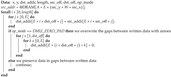 |
4. Evaluation and Results
4.1. Experimental Methodology
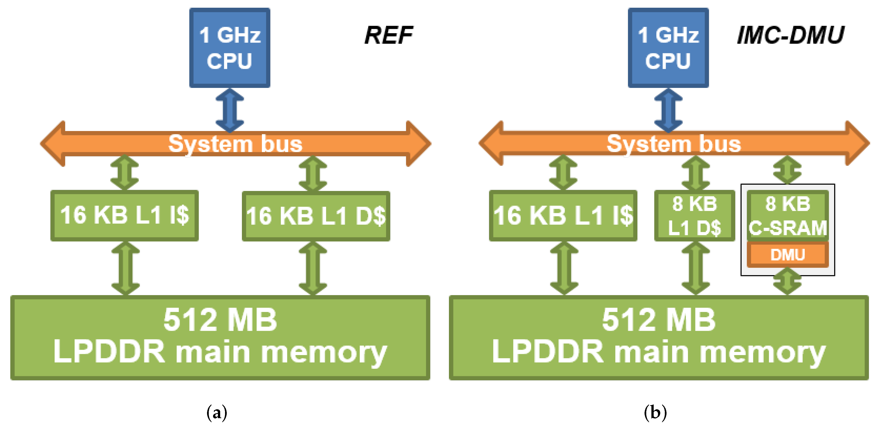
Figure 5a,b present, respectively, the reference and the experimental architecture for the evaluation. The reference architecture is a 1 GHz in-order scalar CPU with a single-level cache hierarchy of 16 kB data and instruction caches, and a 512 MB LP-DDR main memory. Our architecture substitutes the 16 kB data cache with an 8 kB data cache, an 8 kB C-SRAM unit and our DMU controller. Both architectures are equivalent in terms of memory capacity but differ by their computation capabilities and the usage of each of their memory units. For each architecture, the cache memories implement a write-through policy to ensure that the written output data are present in the main memory.
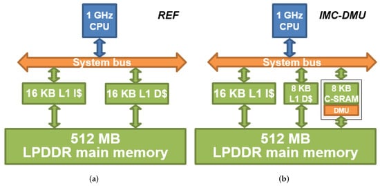
Figure 5.
Experimental memory architectures for the evaluation. All cache units have write-through policy. Our proposed architecture substitutes the 16 kB L1 D with an 8 kB L1 D, an 8 kB C-SRAM and a DMU. (a) Reference architecture; (b) proposed architecture.
Our simulation methodology is based on QEMU in order to perform system-level modeling and evaluation while performing ISA exploration for IMC as well as our DMU instruction [13]. We describe and generate events to model the energy and latency costs of our architecture, from CPU and IMC to the main memory and the cache hierarchy. Table 2 shows the memory parameters of, respectively, the reference architecture and our proposed IMC architecture. These parameters were extracted using CACTI [14] and the characterizations from [2]. Though the specifications of the C-SRAM architecture do not define fixed dimensions, e.g., a fixed row size and number of rows, we consider a 128-bit C-SRAM architecture for the rest of this paper.
Table 2.
Memory parameters of the reference and proposed architecture, used for the experimental evaluation.
4.2. Applications
We consider three applications to evaluate our proposed architecture (IMC-DMU) versus the reference scalar architecture (REF):
- Frame differencing is used in computer vision to perform motion detection [15], and performs saturated subtraction between two (or more) consecutive frames in a video stream to highlight pixel differences. It has linear complexity in both computing and memory.
- A Sobel filter applies two convolution kernels on an input image to generate its edge-highlighted output. It is a standard operator in Image processing as well as computer vision to perform edge detection [16]. It has linear arithmetic complexity and shows constant data redundancy ( reads per input pixel, on average).
- Matrix-matrix multiplication is used in various domains such as signal processing or physics modeling, and is a standard of linear algebra as the gemm operator [17]. It has cubic () complexity in computing and memory and shows quadratic () data redundancy.
4.3. DMU Programming and Data Optimization
Iterative codes using complex patterns such as convolution windows often require streams of consecutive and redundant data to be transferred and aligned before computation according to the mapping scheme of IMC. To reduce the overall transfer latency to populate IMC with said data, we use READ_TRANSFER to copy nonpresent data from the DRAM to IMC and COPY to directly duplicate redundant data instead of accessing the DRAM memory.
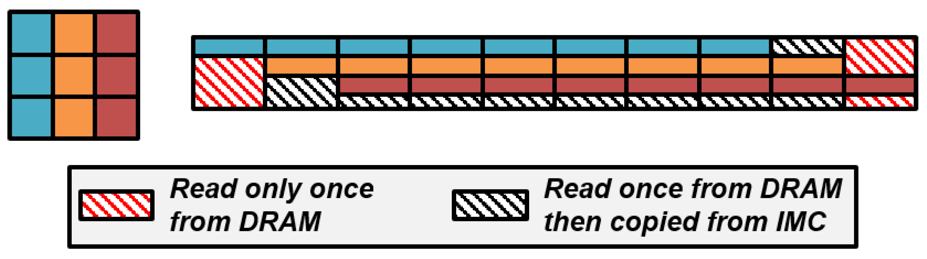
Figure 6 shows the memory access patterns performed for convolution windows at stride 1, each element but the very first and last on each row of the image during the visit is read from the DRAM only once. The rest at some point can be directly read from the C-SRAM to reduce the overall transfer latency. Figure 7 implements the data management described in Figure 6. This technique can be applied to other iterative codes such as stencils, though the appropriate address generations require effort from developers. We are currently developing a mechanism to automatically generate data transfers and duplication from programmable memory access patterns to effortlessly achieve quasi-optimal energy efficiency. We will soon publish our specifications and our results.
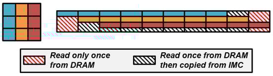
Figure 6.
A stream of convolution windows, transferred row-major, shows opportunities of data duplication to reduce transfer latency.
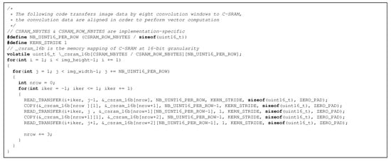
Figure 7.
Example code transferring convolution windows to C-SRAM using our DMU instruction set.
4.4. Results and Discussion
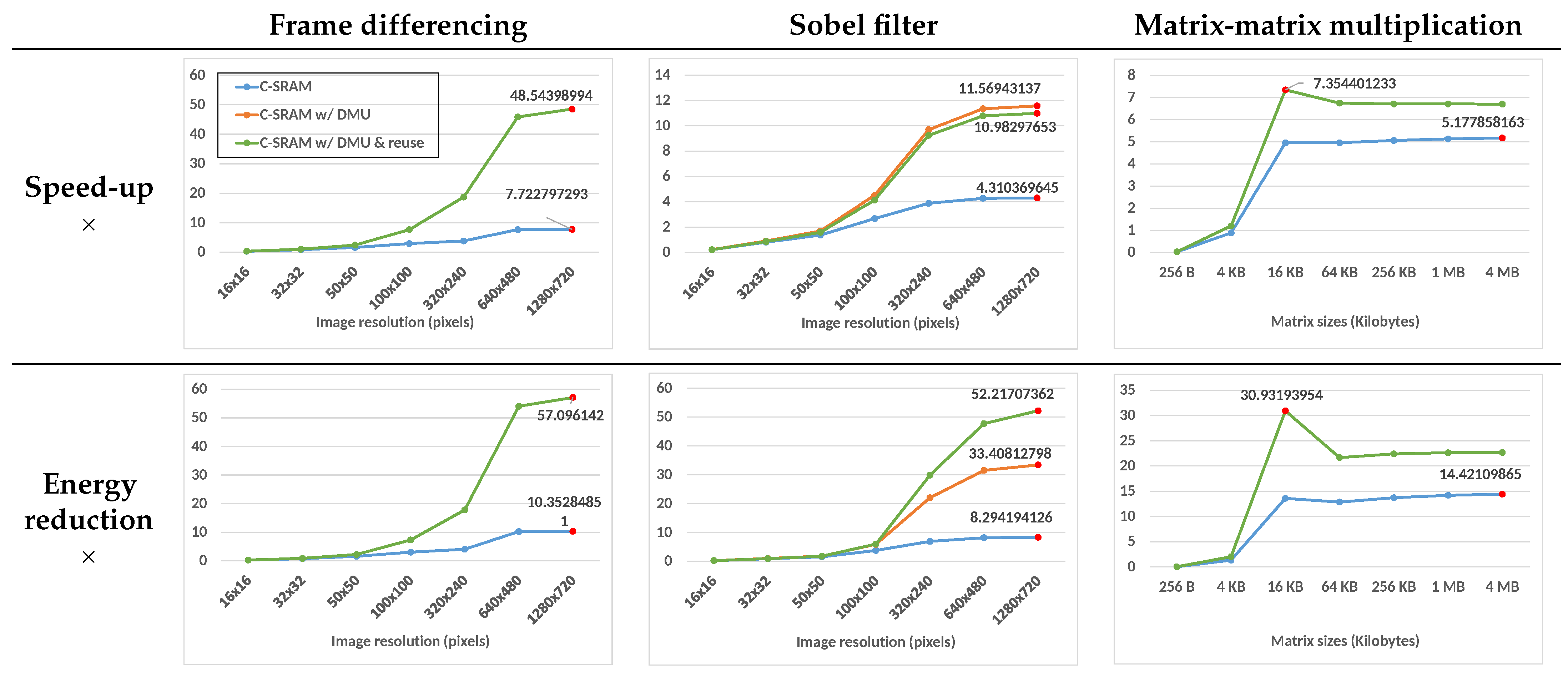
We evaluated the performance of our proposed architecture, according to a reference architecture, in terms of speed-ups and energy reductions. We considered three scenarios: (1) using the C-SRAM without DMU (C-SRAM-only), (2) using the C-SRAM with the proposed DMU controller to fetch input data strictly from the main memory and (C-SRAM+DMU) and (3) using the C-SRAM with the proposed DMU controller to perform data transfers and data reuse whenever possible. In case 1, the data are transferred from the L1 data cache to the C-SRAM by the CPU, while in cases 2 and 3, the CPU issues data transfers directly between the main memory and the C-SRAM using the DMU. Case 3 is particularly relevant to the Sobel filter, which presents data redundancy due to the application of the convolution filters on the input images.
Figure 8 shows the energy reduction and speed-up for the three applications, compared to the reference scalar architecture. The X-axis represents the size of the inputs, and Y-axis represents the improvement factors evaluated for each application (higher is better). Table 3 shows the average of the maximum speed-up and energy reductions evaluated for each implementation across all applications. While the C-SRAM-only implementation shows improvement compared to the scalar system, the integration of the DMU to the C-SRAM improves the speed-up and energy reduction, respectively, from and to and .
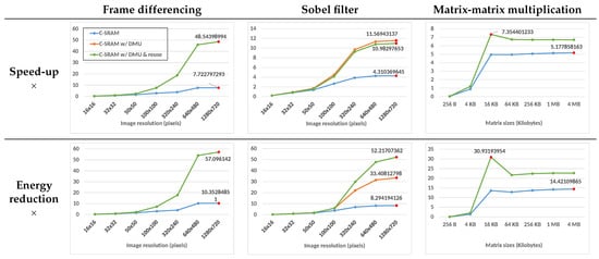
Figure 8.
Energy reduction and speed-up for all applications compared to the reference scalar architecture. The X and Y axes of the plots are, respectively, the data sizes and the improvement factors, i.e., higher is better.
Table 3.
Average maximum speed-up and energy reduction per evaluated implementation.
4.4.1. Frame Differencing
We observe that both the speed-up and the energy reduction are similar without and with the DMU for small resolutions, but are significantly improved by using the DMU starting image resolution, with peak factors achieved of, respectively, and , compared to and when using only the C-SRAM. Because the DMU offers a direct transfer bus between the main memory and C-SRAM, the entirety of the input data can be fetched directly from the C-SRAM without generating as much conflict misses on the L1 data cache. Our hypothesis is supported by the performance gap between the C-SRAM-only and the C-SRAM + DMU implementation getting wider as the images get larger starting resolution. The input and output sizes become too large for the L1 data cache.
4.4.2. Sobel Filter
Similar to frame differencing, the speed-up and energy consumption of the Sobel filter is consistently improved by the DMU. In addition, the Sobel filter offers the opportunity to perform data reuse between consecutive convolution windows by reading part of their components directly from the C-SRAM instead of the main memory. By using the DMU without reusing data, the peak speed-up and energy reduction compared to the reference scalar architecture is and , while the data reuse implementation shows factors of and , which shows a trade-off between the execution performance of C-SRAM + DMU and its energy efficiency. This trade-off is explained by the overhead of the address generation algorithm required for IMC data duplication. The overhead might change depending on the implementation of the algorithm and the CPU performance.
4.4.3. Matrix-Matrix Multiplication
The overall performance of matrix-matrix multiplication is almost similar with and without DMU on small matrices. However, for both implementations the speed-up and energy reduction compared to the reference architecture improve significantly starting from 16 kB matrices, to, respectively, and for the C-SRAM + DMU implementation. The improvement factors are higher for C-SRAM + DMU at this input size because only one of the two operand matrices is transferred through the L1 data cache in this implementation, contrary to the C-SRAM-only implementation, which transfers all input and output matrices through the L1 data cache. Furthermore, the performance drops for both implementations at a 64 kB input size, because the capacity of the L1 data cache has been attained on the experimental architecture to store the first operand matrix. The fact that this drop is more significant for the C-SRAM + DMU implementation compared to the C-SRAM-only variant shows the impact of the cache hierarchy on the performance of IMC architectures without any dedicated transfer mechanism.
5. Conclusions
We presented the DMU, a programmable memory controller architecture to efficiently transfer and reorganize data between the SRAM IMC memory and the main memory. We integrated the DMU in a C-SRAM architecture and evaluated the energy reduction and speed-up for three applications, compared to a reference scalar architecture. The integration of the DMU to C-SRAM improved the speed-up and energy reduction, respectively, from and to and .
Our future works include the physical implementation of the DMU on a test chip for the validation of our experiments and the compiler support of its ISA to implement an efficient programming model at the language level. We also plan to describe the specifications of a more elaborate instruction set, able to transfer complex data structures such as stencil kernels and convolution windows using pattern descriptors, in order to automate transfer optimizations at the hardware level.
Author Contributions
Conceptualization, K.M., H.-P.C., M.K. and J.D.; methodology, all authors; software, all authors; validation, all authors; formal analysis, all authors; investigation, all authots; resources, all authors; data curation, all authots; writing—original, K.M.; writing—review and editing, H.-P.C., M.K. and J.D.; visualization, all authors; supervision, H.-P.C. and M.K.; project administration, H.-P.C. and M.K.; funding acquisition, H.-P.C. and M.K. All authors have read and agreed to the published version of the manuscript.
Funding
This work was supported by the EU H2020 project 955606 “DEEPSEA” – Software for Exascale Architectures.
Data Availability Statement
Not applicable.
Conflicts of Interest
The authors declare no conflict of interest.
References
- Horowitz, M. 1.1 Computing’s energy problem (and what we can do about it). In Proceedings of the 2014 IEEE International Solid-State Circuits Conference Digest of Technical Papers (ISSCC), San Francisco, CA, USA, 9–13 February 2014; pp. 10–14. [Google Scholar]
- Noel, J.P.; Pezzin, M.; Gauchi, R.; Christmann, J.F.; Kooli, M.; Charles, H.P.; Ciampolini, L.; Diallo, M.; Lepin, F.; Blampey, B.; et al. A 35.6 TOPS/W/mm² 3-Stage Pipelined Computational SRAM with Adjustable Form Factor for Highly Data-Centric Applications. IEEE Solid-State Circuits Lett. 2020, 3, 286–289. [Google Scholar] [CrossRef]
- Kooli, M.; Charles, H.P.; Touzet, C.; Giraud, B.; Noel, J.P. Smart Instruction Codes for In-Memory Computing Architectures Compatible with Standard SRAM Interfaces. In Proceedings of the 2018 Design, Automation & Test in Europe Conference & Exhibition (DATE), Dresden, Germany, 19–23 March 2018; p. 6. [Google Scholar]
- Gauchi, R.; Egloff, V.; Kooli, M.; Noel, J.P.; Giraud, B.; Vivet, P.; Mitra, S.; Charles, H.P. Reconfigurable tiles of computing-in-memory SRAM architecture for scalable vectorization. In Proceedings of the ACM/IEEE International Symposium on Low Power Electronics and Design, Boston, MA, USA, 10–12 August 2020; pp. 121–126. [Google Scholar]
- Bavikadi, S.; Sutradhar, P.R.; Khasawneh, K.N.; Ganguly, A.; Pudukotai Dinakarrao, S.M. A Review of In-Memory Computing Architectures for Machine Learning Applications. In Proceedings of the 2020 on Great Lakes Symposium on VLSI, Virtual, China, 7–9 September 2020; pp. 89–94. [Google Scholar]
- Seshadri, V.; Lee, D.; Mullins, T.; Hassan, H.; Boroumand, A.; Kim, J.; Kozuch, M.A.; Mutlu, O.; Gibbons, P.B.; Mowry, T.C. Ambit: In-Memory Accelerator for Bulk Bitwise Operations Using Commodity DRAM Technology. In Proceedings of the 2017 50th Annual IEEE/ACM International Symposium on Microarchitecture (MICRO), Boston, MA, USA, 14–17 October 2017; pp. 273–287. [Google Scholar]
- Deng, Q.; Zhang, Y.; Zhang, M.; Yang, J. LAcc: Exploiting Lookup Table-based Fast and Accurate Vector Multiplication in DRAM-based CNN Accelerator. In Proceedings of the 56th Annual Design Automation Conference, Las Vegas, NV, USA, 2–6 June 2019; pp. 1–6. [Google Scholar]
- Fujiki, D.; Mahlke, S.; Das, R. Duality Cache for Data Parallel Acceleration. In Proceedings of the 46th International Symposium on Computer Architecture, Phoenix, AZ, USA, 22–26 June 2019; pp. 1–14. [Google Scholar]
- Lee, K.; Jeong, J.; Cheon, S.; Choi, W.; Park, J. Bit Parallel 6T SRAM In-memory Computing with Reconfigurable Bit-Precision. In Proceedings of the 2020 57th ACM/IEEE Design Automation Conference (DAC), San Francisco, CA, USA, 20–24 July 2020; pp. 1–6. [Google Scholar]
- Bhattacharjee, D.; Devadoss, R.; Chattopadhyay, A. ReVAMP: ReRAM based VLIW architecture for in-memory computing. In Proceedings of the Design, Automation & Test in Europe Conference & Exhibition (DATE), Lausanne, Switzerland, 27–31 March 2017; pp. 782–787. [Google Scholar]
- Ezzadeen, M.; Bosch, D.; Giraud, B.; Barraud, S.; Noel, J.P.; Lattard, D.; Lacord, J.; Portal, J.M.; Andrieu, F. Ultrahigh-Density 3-D Vertical RRAM with Stacked Junctionless Nanowires for In-Memory-Computing Applications. IEEE Trans. Electron Devices 2020, 67, 4626–4630. [Google Scholar] [CrossRef]
- Ahn, J.; Yoo, S.; Mutlu, O.; Choi, K. Pim-enabled instructions: A low-overhead, locality-aware processing-in-memory architecture. In Proceedings of the 2015 ACM/IEEE 42nd Annual International Symposium on Computer Architecture (ISCA), Portland, OR, USA, 13–17 June 2015; pp. 336–348. [Google Scholar]
- Mambu, K.; Charles, H.-P.; Dumas, J.; Kooli, M. Instruction Set Design Methodology for In-Memory Computing through QEMU-Based System Emulator. 2021. Available online: https://hal.archives-ouvertes.fr/hal-03449840/document (accessed on 14 December 2021).
- Muralimanohar, N.; Balasubramonian, R.; Jouppi, N.P. Cacti 6.0: A Tool to Model Large Caches; HP Laboratories: Palo Alto, CA, USA, 2009. [Google Scholar]
- Zhang, H.; Wu, K. A Vehicle Detection Algorithm Based on Three-Frame Differencing and Background Subtraction. In Proceedings of the 2012 Fifth International Symposium on Computational Intelligence and Design, Hangzhou, China, 28–29 October 2012; Volume 1, pp. 148–151. [Google Scholar]
- Khronos Vision Working Group. The OpenVX Specification Version 1.2. Available online: https://www.google.co.th/url?sa=t&rct=j&q=&esrc=s&source=web&cd=&cad=rja&uact=8&ved=2ahUKEwjB65aM0sn2AhUkxzgGHa-sDlMQFnoECAgQAQ&url=https%3A%2F%2Fwww.khronos.org%2Fregistry%2FOpenVX%2Fspecs%2F1.2%2FOpenVX_Specification_1_2.pdf&usg=AOvVaw18k11o92s0PEjGw7rZ5Sm8 (accessed on 11 October 2017).
- Basic Linear Algebra Subprograms Technical (BLAST) Forum Standard, Basic Linear Algebra Subprograms Technical Forum. Available online: https://www.google.co.th/url?sa=t&rct=j&q=&esrc=s&source=web&cd=&cad=rja&uact=8&ved=2ahUKEwj6orG00sn2AhU_zjgGHcvDADoQFnoECAgQAQ&url=http%3A%2F%2Fwww.netlib.org%2Futk%2Fpeople%2FJackDongarra%2FPAPERS%2F135_2002_basic-linear-algebra-subprograms-techinal-blas-forum-standard.pdf&usg=AOvVaw3GQ_wyRmkgT9TG9mwuCS0I (accessed on 21 August 2001).

Publisher’s Note: MDPI stays neutral with regard to jurisdictional claims in published maps and institutional affiliations. |
© 2022 by the authors. Licensee MDPI, Basel, Switzerland. This article is an open access article distributed under the terms and conditions of the Creative Commons Attribution (CC BY) license (https://creativecommons.org/licenses/by/4.0/).