Article

Stable Electron Concentration Si-doped β-Ga2O3 Films Homoepitaxial Growth by MOCVD

State Key Laboratory on Integrated Optoelectronics, College of Electronic Science and Engineering, Jilin University, Qianjin Street 2699, Changchun 130012, China
*
Author to whom correspondence should be addressed.
Coatings 2021, 11(5), 589; https://doi.org/10.3390/coatings11050589
Submission received: 7 April 2021 / Revised: 12 May 2021 / Accepted: 13 May 2021 / Published: 17 May 2021
(This article belongs to the Special Issue Epitaxial Thin Films: Properties and Applications)

Abstract

:
To obtain high-quality n-type doped β-Ga2O3 films, silane was used as an n-type dopant to grow Si-doped β-Ga2O3 films on (100) β-Ga2O3 substrates by metal-organic chemical vapor deposition (MOCVD). The electron concentrations of the Si-doped β-Ga2O3 films obtained through experiments can be stably controlled in the range of 6.5 × 1016 cm−3 to 2.6 × 1019 cm−3, and the ionization energy of Si donors is about 30 meV, as determined by analysis and calculation. The full width at half maxima of the rocking curves of the (400) crystal plane of all doped films was less than 500 arcsec, thus showing high crystal quality, while the increase of the doping concentration increased the defect density in the β-Ga2O3 films, which had an adverse effect on the crystal quality and surface morphology of the films. Compared with heteroepitaxial Si-doped β-Ga2O3 films, homoepitaxial Si-doped β-Ga2O3 films exhibited higher quality, lower defect density, and more stable electron concentration, which make them more conductive for preparing Ga2O3-based power devices.

1. Introduction

Ga2O3 is an ultra-wide band gap semiconductor material. As the most stable phase of Ga2O3, β-Ga2O3 has become one of the most promising semiconductor materials for power devices due to its band gap of 4.9 eV, its breakdown electric field of 8 MV/cm, and its Barriga figure of merit of 3444 [1]. In addition, β-Ga2O3 has high transmittance to UV–visible light and sensitivity to a variety of gases [2], which makes β-Ga2O3 at the forefront of development in the field of light detection, light-emitting devices, and gas sensing [3,4,5,6,7,8,9]. Great progress has been made recently in large-sized Ga2O3 single crystal preparation, which provides favorable support for the preparation of device-applied Ga2O3 films by homoepitaxy [10,11]. Ga2O3-based devices with excellent performance require the films to not only have higher crystal quality but also stable and controllable carrier concentration. Therefore, obtaining a stable carrier concentration of β-Ga2O3 films is the key step in Ga2O3-based device fabrication [12]. The Si is considered as a reliable n-type doping source for its good stability. However, according to an earlier report [13], the stability of electrical properties of β-Ga2O3 films is greatly affected by intrinsic defects, which is detrimental to the performance of Ga2O3 devices. This problem has not been solved yet at present.
In this article, Si-doped β-Ga2O3 films are grown on (100) Ga2O3 substrates by MOCVD. The films with different Si-doping concentrations are measured and analyzed.

2. Materials and Methods

2.1. Materials

In the experiment, the (100) β-Ga2O3 substrates were prepared by floating zone melting. High-purity O2 (5N) and trimethylgallium (TMGa, 6N) were used as an oxygen source and metal organic source, respectively. Silane (SiH4; diluent: high-purity N2; 50 ppm) was used as the n-type doping source. High-purity Ar (5N) worked as the carrier gas.

2.2. Experiment

Before the experiment, the substrates were ultrasonically cleaned by acetone, ethanol, and deionized water for 5 min in turn, then dried with N2 and placed in the MOCVD reaction chamber. The MOCVD system used was the Emcore-D180 (Emcore, Alhambra, CA, USA). The TMGa in the stainless-steel bubbler was maintained at 1 °C by a water bath. During the growth process, we kept the temperature and pressure of the reaction chamber at 750 °C and 40 mbar. The flow rates of O2 and Ar were set to 400 sccm and 60 sccm, respectively. Growth time was set to 1 h. β-Ga2O3 films with different doping concentrations were obtained by setting the SiH4 flow rate to increase from 0 to 14 sccm (0, 2, 4, 6, 8, 10, 14 sccm).

2.3. Characterization

The crystal structure and quality of the films were characterized by X-ray diffraction and grazing incidence X-ray diffraction (XRD and GIXRD; Rigaku, Ultima IV, Tokyo, Japan, λ = 1.54 Å). A field emission scanning electron microscope (FESEM, JOEL, JSM-7610, Tokyo, Japan) and an atomic force microscope (AFM, Veeco, PlainView, NY, USA) were used to observe the surface morphology of the films. The optical properties of the films were characterized by a photoluminescence system consisting of a spectrometer (Horiba, iHR550, Paris, France) and a YAG laser, with an excitation wavelength of 235 nm. The carrier concentrations of the films were measured by a Hall effect device (Accent, HL5500PC, Hertfordshire, UK).

3. Results

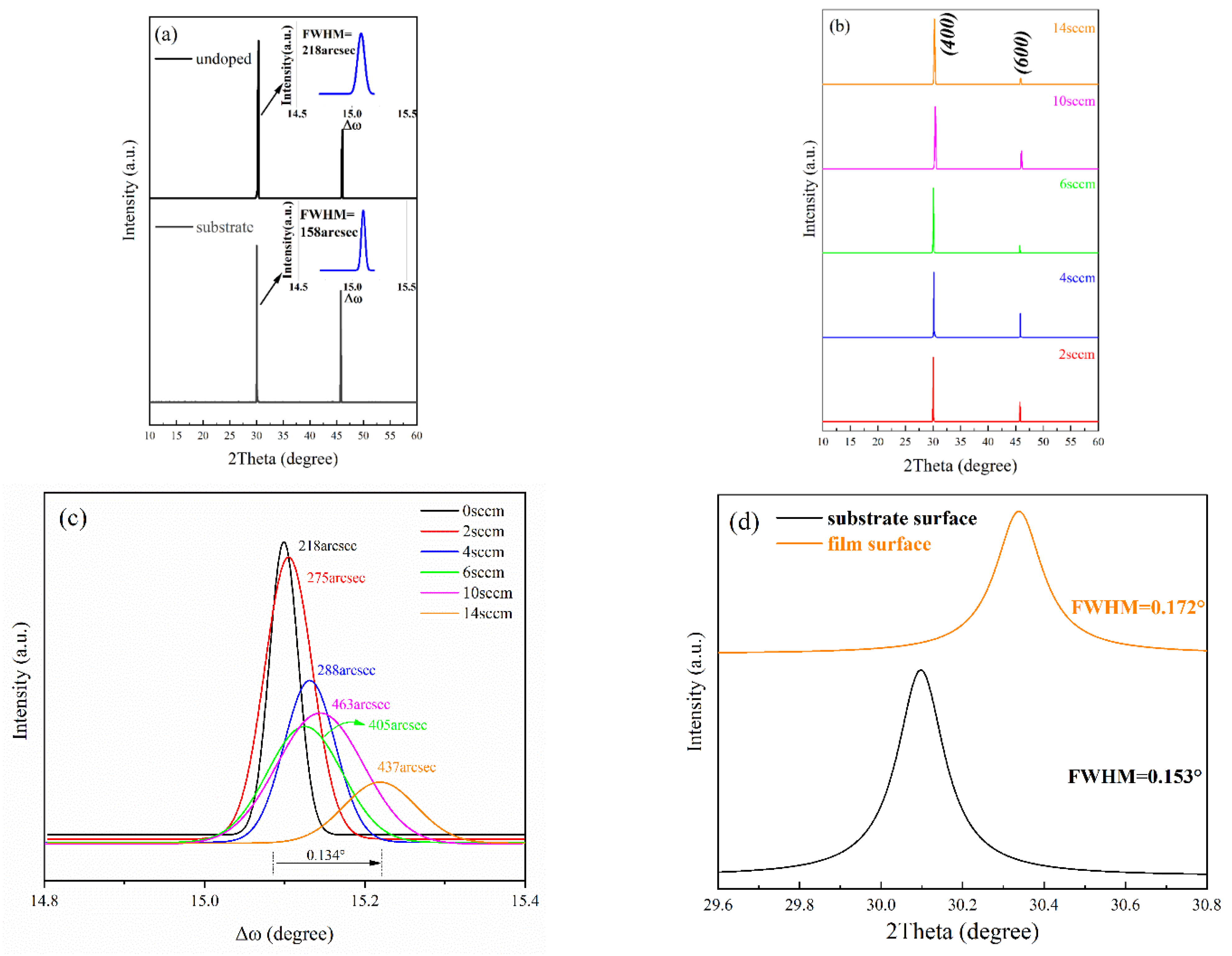
3.1. Crystal Structure Analysis

Figure 1 shows the 2θ–ω scan curve and the double crystal rocking curve of the β-Ga2O3 substrate and the films obtained under different SiH4 flow rate. From Figure 1a, the crystal quality of the β-Ga2O3 film is slightly degraded compared to the substrate. The full width at half maxima (FWHM) of film is 218 arcsec, which is slightly higher than the 158 arcsec of the substrate, which is consistent with previous reports [14]. As shown in Figure 1b, all doped β-Ga2O3 films only exhibit sharp diffraction peaks corresponding to (400) and (600) planes, which indicates that the doped β-Ga2O3 films still present high crystal quality. Figure 1c shows the (400) double crystal rocking curve of β-Ga2O3 films with different SiH4 flow rates. From the figure, with the increase of SiH4 flow rate, the relative intensity of the rocking curve peak decreases and the FWHM increases gradually (from 218 to 463 arcsec). The diffraction peak is found shifted by 0.134° to a high angle. This can be explained by the fact that the migration speed of the Ga and O atoms on the surface of the films during the growth process is affected by the doped Si atoms. This in turn changes the energy distribution in different growth directions and leads to the weakening of the (100) directional growth. In addition, because the Si4+ radius (0.041 nm) is smaller than the Ga3+ radius (0.062 nm), the lattice constant decreases after the atom Si replaces Ga, which is consistent with the Scherer’s formula shown in Equation (1) [15]:
D = K γ B cos θ
where K is the Scherrer constant (K = 0.89), D is the average thickness of the crystal grain perpendicular to the crystal plane, B is the FWHM of the rocking curve of (400) crystal plane, θ is the Bragg angle, and γ is the X-ray wavelength (γ = 1.54 Å).
In the above XRD analysis, the diffraction peaks of the film and those of the substrate overlapped due to the large penetration depth of X-rays. Therefore, The GIXRD was performed separately on the substrate surface and on the surface of the film obtained at a SiH4 flow rate of 14 sccm. The grazing incidence angle was set to 0.3°, and the result is shown in Figure 1d. Compared with the substrate surface, the diffraction peak of the (400) interference surface of the film surface obviously shifted to a higher angle, and the FWHM was slightly increased. This reveals the change in diffraction peaks formed by the superposition of the substrate and the film, which originated in the change in the quality of the film.

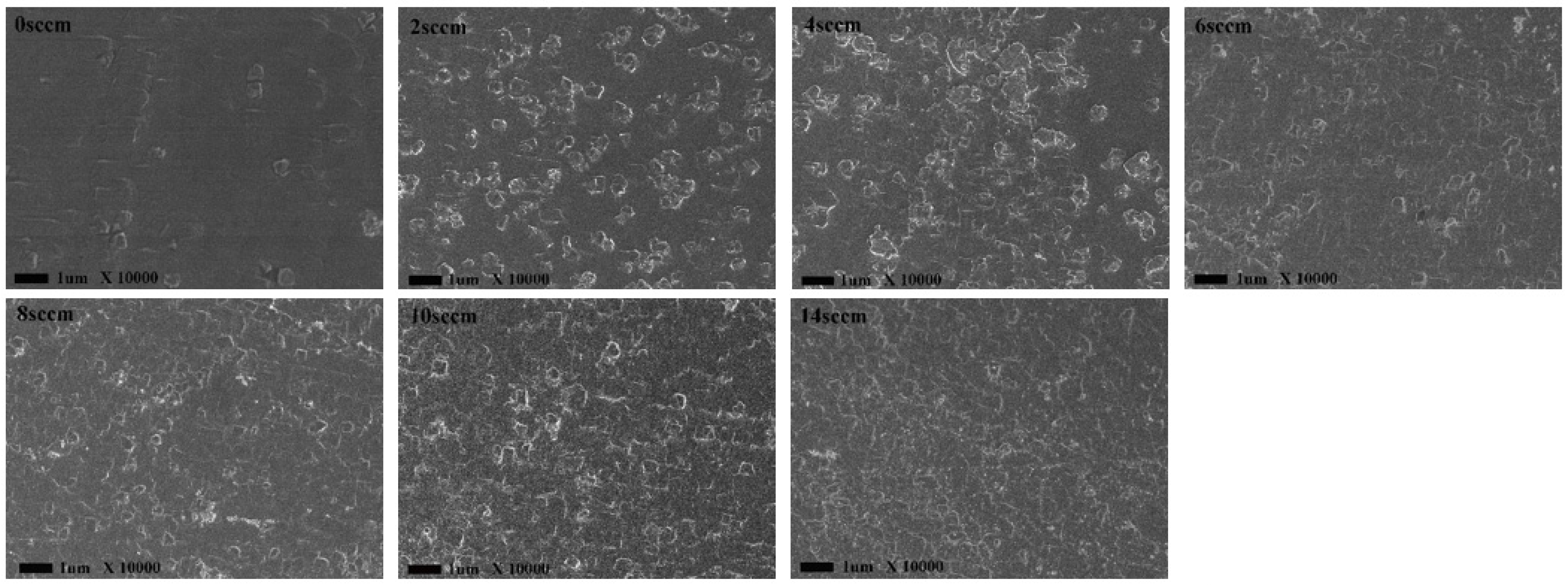
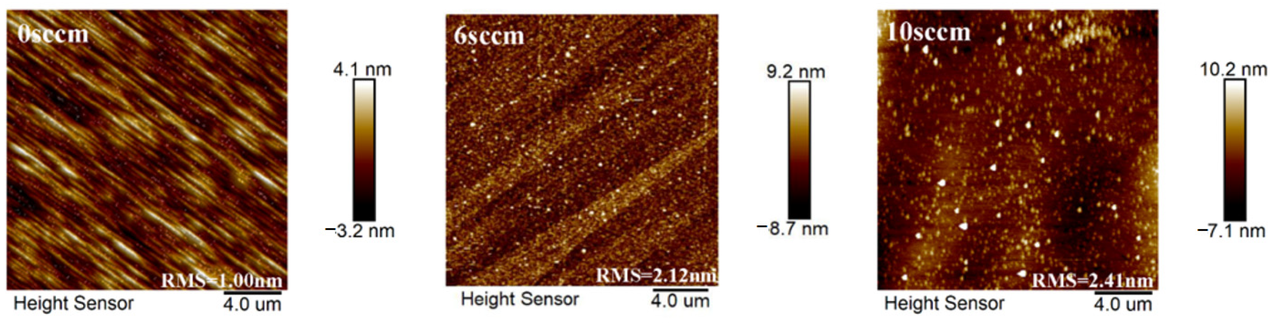
3.2. Surface Morphological Analysis

Figure 2 shows the SEM images of the doped β-Ga2O3 films obtained under different SiH4 flow rates. It can be seen that the surface morphology of the films strongly depends on the Si-doping concentration. The surface of the undoped sample is flat and compact. Numerous hexagon columns in the same direction can be found connected horizontally. It should be noted that a lot of protrusions appear on the surface when the doping concentration increases. The number of protrusions increase significantly, resulting in the films surface becoming rough and disordered gradually. According to our previous research [16], the growth rate of unintentionally doped (UID) β-Ga2O3 films was about 300 nm/30 min under the same conditions. Therefore, it can be estimated that the thickness of the doped β-Ga2O3 films obtained in this experiment is about 600 nm.
To further characterize the three-dimensional morphology of the films surface, the β-Ga2O3 films were characterized by AFM, as shown in Figure 3. As the flow rate of SiH4 increased from 0 to 10 sccm, the root mean square (RMS) roughness of the films increased from 1.00 to 2.41 nm. The diameter of the protrusions on the surface of the films increased significantly, which was mainly caused by the mutual stacking of protrusions. It is worth noting that the surface of the films obtained at a SiH4 flow rate of 0 sccm and 6 sccm was composed of multiple bands, which is probably caused by the step growth mode of the films. This is quite different from the film surface obtained at a SiH4 flow rate of 10 sccm. Combining the SEM and AFM analysis, it can be concluded that the introduction of Si atoms can greatly affect the film growth process and even change the film growth mode, resulting in the deterioration of the film surface, especially for processes with slow films growth rates such as MOCVD.

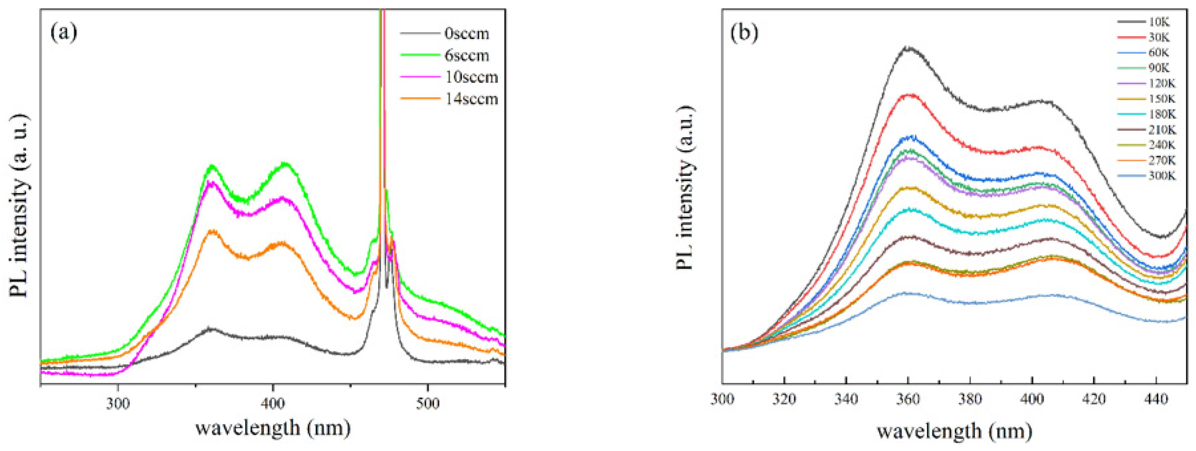
3.3. PL Characteristics Analysis

The PL spectrums of β-Ga2O3 films are shown in Figure 4. Figure 4a is the room temperature PL spectrums of β-Ga2O3 films obtained under different SiH4 flow rates. From the figure, in addition to excitation light, two main emission bands at 360 and 410 nm can be observed. The UV peak (≈360 nm) is formed by the radiation combination of self-trapped holes (STHs) and electrons [17,18,19], and the blue peak (≈410 nm) is related to the radiation recombination of the donor–acceptor pairs [20,21]. The donors in the undoped β-Ga2O3 films were mainly oxygen vacancies (VO) and interstitial gallium (Gai), while Si donors are the mainly donors in the Si-doped β-Ga2O3 films, followed by VO and Gai. The acceptors in the β-Ga2O3 films are mainly gallium vacancies (VGa) and gallium–oxygen vacancies pairs (VGa–VO) [22]. The intensities of the two emission peaks of the doped β-Ga2O3 films are stronger than that of the undoped film. This is because compared to the undoped β-Ga2O3 films, the Si donor levels in the doped films can excite more electrons that participate in radiative recombination. In addition, the emission intensities of the doped β-Ga2O3 films are negatively correlated with the SiH4 flow rate. The increase in doping concentration increases the defect density in the films, thus introducing more defect levels into the band gap, which leads to the enhancement of a nonradiative recombination of electrons and holes on donor, acceptor, and defect levels. The increase in defect density is one of the reasons for the deterioration of the crystal quality of doped β-Ga2O3 films, which is consistent with the conclusion of XRD analysis.
The doped β-Ga2O3 film obtained at a SiH4 flow rate of 6 sccm exhibited the highest photoluminescence intensity at room temperature. Therefore, a temperature-dependent PL was performed on the film obtained under this condition to test the relationship between the luminescence characteristics and the temperature. The result is shown in Figure 4b. The emission intensities of UV and blue peaks were the strongest when the temperature was 10 K. As the temperature increased, the emission intensities gradually decreased. This is because the higher temperature can aggravate the thermal decomposition of STHs and can make the electrons and holes on the donor and acceptor levels excited to the conduction band and valence band, respectively. However, compared to UV peak, the intensity of blue peak decreased more slowly, and so the emission intensity of the blue peak was higher than that of UV peak at room temperature. This shows that STHs are more severely affected by temperature. β-Ga2O3 exhibits complex PL behavior because of its low-symmetry structure and the existence of trapped polarons [23,24].

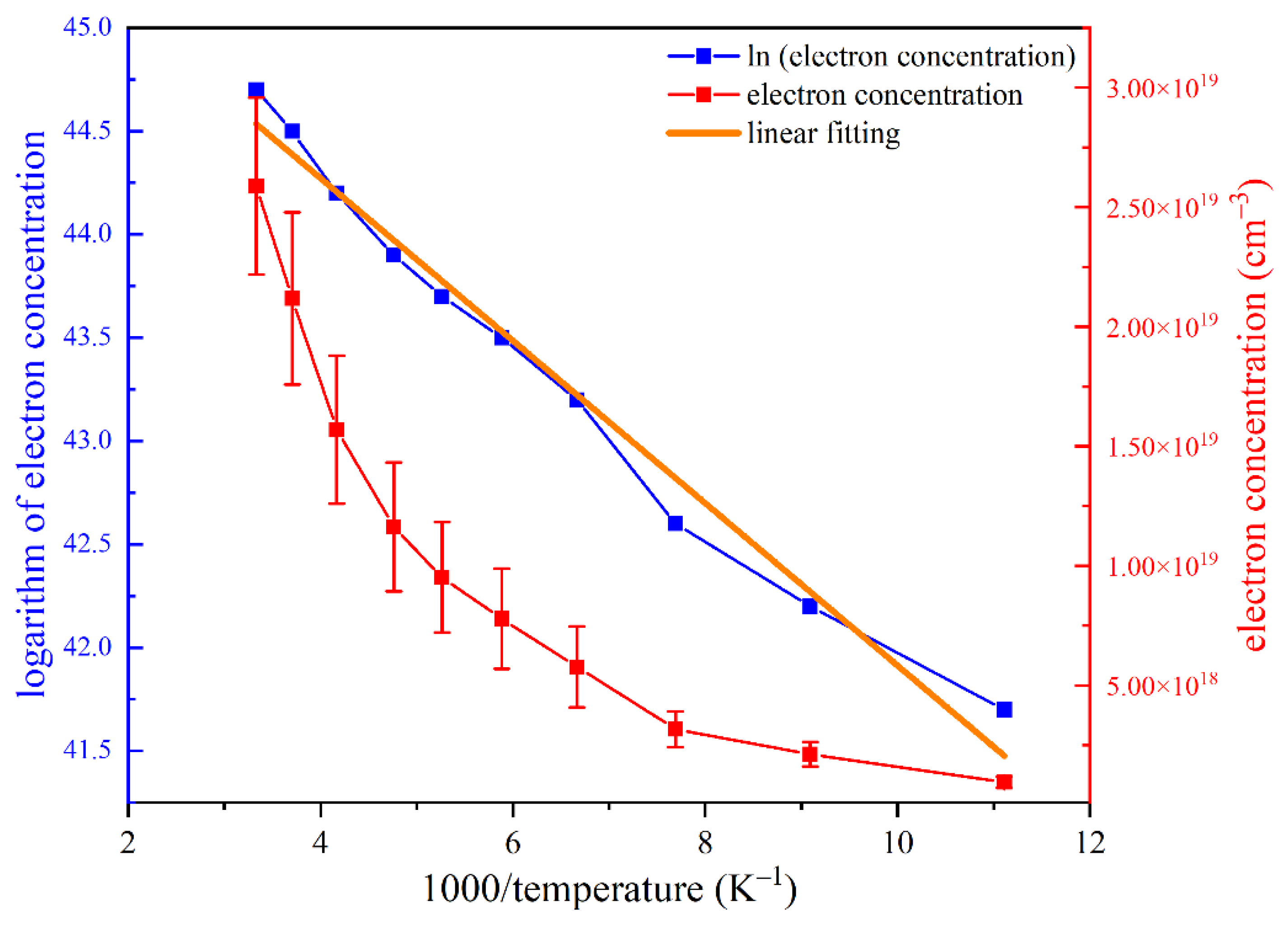
3.4. Electron Concentration Analysis

To reduce the inaccuracy caused by the numerical fluctuations in the results of the hall test, we conducted three tests on each film and calculated the average and standard error of the results. The averages of electron concentrations of films are shown in Table 1. From the table, the electron concentrations increase with the increase of the SiH4 flow rates [25,26], but it should be noted that the increase rates of electron concentrations gradually decrease. This is mainly because the effective electron concentration is limited by the solubility of the dopant in a higher SiH4 flow rate, or the secondary phase of the oxide [23,27]. To evaluate the effect of defects’ density, especially the VO or Gai, the oxygen annealing was performed at 900 °C for one hour. Figure 5 exhibits the error bar of the electron concentrations of the films grown under different SiH4 flow rates before and after annealing. The electron concentrations of the annealed films had a slight decrease compared to the as-grown films. The decrease was much slighter than that of heteroepitaxial β-Ga2O3 films [28], which indicates that the homoepitaxial films have lower defect density. Although the annealing process did not have an obvious effect for the high crystal quality of the films, the electrical stability of the films can be improved to a certain extent.
In addition, a temperature-dependent electron concentration test was conducted on the β-Ga2O3 film obtained at a SiH4 flow rate of 14 sccm to further study the stability of the electrical properties of the films. The error bar of the results is shown in Figure 6. It can be found from the red curve in the figure that as the temperature decreased, the electron concentrations of the film decreased significantly. Within the test temperature range, the electron concentrations of the film differed by an order of magnitude. The relationships between the ionization energy of the donors and the electron concentrations are exhibited in Equations (2) and (3).
N = N 0 e Δ E k T
l n N = l n N 0 Δ E 1000 k 1000 T
where N is the electron concentrations, ΔE is the ionization energy of the donors, and k is the Boltzmann constant. The relationship between lnN and 1000/T is shown in the blue curve in Figure 6. The yellow curve in Figure 6 is the result of linear fitting to the blue curve. According to the slope of the yellow curve, the donors ionization energy of the film is about 30 meV.
To verify the stability of the electron concentrations of the films, the Hall tests were performed again on the β-Ga2O3 films two months later (shown in Table 2). It was found that compared to the results obtained two months ago, the electron concentrations of the films fluctuate in a small range, but the order of magnitudes of the electron concentrations remain the same, indicating that the films have low defect densities and the electron concentrations are less affected by the environment.

4. Conclusions

The stable electron concentration Si-doped β-Ga2O3 films were grown on (100) β-Ga2O3 single crystal substrates by MOCVD. The electron concentrations of the films can be reasonably controlled by adjusting the SiH4 flow rate. During the growth process, the Si atoms changed the migration rate of the Ga atom and the O atom, which changed the energy distribution of the atoms, resulting in the growth weakening of (100) orientation and the enhancement of the surface morphology disorder. The temperature-dependent hall effect test showed that the ionization energy of Si donors was about 30 meV. In addition, the defect density in the films increased with the increase of the doping concentration, thereby weakening the PL emission intensity. The temperature-dependent PL showed that PL emission intensity is closely related to temperature. High temperature can accelerate the thermal desorption of STHs and make the electrons and holes on the donor and acceptor levels excited to the conduction band and valence band, respectively, thus reducing the radiation recombination intensity. Si-doped n-type homoepitaxial β-Ga2O3 with high crystal quality and stable electron concentration can be obtained, which offers an effective method to fabricate the Ga2O3-based devices.

Author Contributions

Conceptualization, T.J. and Z.L. (Zeming Li); methodology, W.C.; software, T.J.; validation, W.C.; formal analysis, Z.D.; investigation, Z.L. (Zeming Li); resources, B.Z.; data curation, Y.Z.; writing—original draft preparation, T.J.; writing—review and editing, X.D.; visualization, Z.L. (Zhengda Li); supervision, X.D.; project administration, X.D.; funding acquisition, X.D. All authors have read and agreed to the published version of the manuscript.

Funding

This research was funded by the National Natural Science Foundation of China, grant numbers 61774072, 61734001, 61574069, and 61674068; the National Key Research and Development Program, grant number 2018YFB0406703; the National Natural Science Foundation of China, Grant Numbers 62074069, 61734001 and 61674068; the Science and Technology Developing Project of Jilin Province, grant number 20200801013GH.

Institutional Review Board Statement

Not Applicable.

Informed Consent Statement

Not Applicable.

Data Availability Statement

Data is contained within the article.

Conflicts of Interest

The authors declare no conflict of interest.

References

  1. Peelaers, H.; Van De Walle, C.G. Brillouin zone and band structure of β-Ga2O3. Phys. Status solidi 2015, 252, 828–832. [Google Scholar] [CrossRef]
  2. Ueda, N.; Hosono, H.; Waseda, R.; Kawazoe, H. Anisotropy of electrical and optical properties in β-Ga2O3 single crystals. Appl. Phys. Lett. 1997, 71, 933–935. [Google Scholar] [CrossRef]
  3. Li, X.; Zhen, X.; Meng, S.; Xian, J.; Shao, Y.; Fu, X.; Li, D. Structuring β-Ga2O3 Photonic Crystal Photocatalyst for Efficient Degradation of Organic Pollutants. Environ. Sci. Technol. 2013, 47, 9911–9917. [Google Scholar] [CrossRef] [PubMed]
  4. Zhong, M.; Wei, Z.; Meng, X.; Wu, F.; Li, J. High-performance single crystalline UV photodetectors of β-Ga2O3. J. Alloy. Compd. 2015, 619, 572–575. [Google Scholar] [CrossRef]
  5. Wang, J.; Ye, L.; Wang, X.; Zhang, H.; Li, L.; Kong, C.; Li, W. High transmittance β-Ga2O3 thin films deposited by magnetron sputtering and post-annealing for solar-blind ultraviolet photodetector. J. Alloy. Compd. 2019, 803, 9–15. [Google Scholar] [CrossRef]
  6. Yang, J.; Ren, F.; Tadjer, M.; Pearton, S.J.; Kuramata, A. 2300V Reverse Breakdown Voltage Ga2O3Schottky Rectifiers. ECS J. Solid State Sci. Technol. 2018, 7, Q92–Q96. [Google Scholar] [CrossRef]
  7. Wong, M.H.; Sasaki, K.; Kuramata, A.; Yamakoshi, S.; Higashiwaki, M. Field-Plated Ga2O3MOSFETs With a Breakdown Voltage of Over 750 V. IEEE Electron. Device Lett. 2016, 37, 212–215. [Google Scholar] [CrossRef]
  8. Kozlov, A.; Krivozubov, O.; Kurdukova, E.; Lila, M. Gas sensors on Ga2O3-In2O3 thin films. In Proceedings of the 2012 28th International Conference on Microelectronics Proceedings, Institute of Electrical and Electronics Engineers (IEEE), Nis, Serbia, 13–16 May 2012; pp. 165–168. [Google Scholar]
  9. Jang, S.B.; Heo, G.-S.; Kim, E.-M.; Park, H.-G.; Lee, J.H.; Jung, Y.H.; Jeong, H.-C.; Han, J.-M.; Seo, D.-S. Homogeneous alignment of liquid crystals on low-temperature solution-derived gallium oxide films via IB irradiation method. Liq. Cryst. 2016, 43, 1–7. [Google Scholar] [CrossRef]
  10. Víllora, E.G.; Shimamura, K.; Yoshikawa, Y.; Aoki, K.; Ichinose, N. Large-size β-Ga2O3 single crystals and wafers. J. Cryst. Growth 2004, 270, 420–426. [Google Scholar] [CrossRef]
  11. Kuramata, A.; Koshi, K.; Watanabe, S.; Yamaoka, Y.; Masui, T.; Yamakoshi, S. High-quality β-Ga2O3single crystals grown by edge-defined film-fed growth. Jpn. J. Appl. Phys. 2016, 55, 1202A2. [Google Scholar] [CrossRef]
  12. Gogova, D.; Schmidbauer, M.; Kwasniewski, A.K. Homo- and heteroepitaxial growth of Sn-doped β-Ga2O3 layers by MOVPE. Cryst. Eng. Comm. 2015, 17, 6744–6752. [Google Scholar] [CrossRef]
  13. Pearton, S.J.; Yang, J.; Iv, P.H.C.; Ren, F.; Kim, J.; Tadjer, M.J.; Mastro, M.A. A review of Ga2O3materials, processing, and devices. Appl. Phys. Rev. 2018, 5, 011301. [Google Scholar] [CrossRef] [Green Version]
  14. Murakami, H.; Nomura, K.; Goto, K.; Sasaki, K.; Kawara, K.; Thieu, Q.T.; Togashi, R.; Kumagai, Y.; Higashiwaki, M.; Kuramata, A.; et al. Homoepitaxial growth of β-Ga2O3layers by halide vapor phase epitaxy. Appl. Phys. Express 2015, 8, 015503. [Google Scholar] [CrossRef]
  15. Li, Z.; Jiao, T.; Yu, J.; Hu, D.; Lv, Y.; Li, W.; Dong, X.; Zhang, B.; Zhang, Y.; Feng, Z.; et al. Single crystalline β-Ga2O3 homoepitaxial films grown by MOCVD. Vacuum 2020, 178, 109440. [Google Scholar] [CrossRef]
  16. O’Leary, S.K.; Foutz, B.E.; Shur, M.S.; Eastman, L.F. Steady-State and Transient Electron Transport Within the III–V Nitride Semiconductors, GaN, AlN, and InN: A Review. J. Mater. Sci. Mater. Electron. 2006, 17, 87–126. [Google Scholar] [CrossRef]
  17. Wang, Y.; Dickens, P.T.; Varley, J.B.; Ni, X.; Lotubai, E.; Sprawls, S.; Liu, F.; Lordi, V.; Krishnamoorthy, S.; Blair, S.; et al. Incident wavelength and polarization dependence of spectral shifts in β-Ga2O3 UV photoluminescence. Sci. Rep. 2018, 8, 1–7. [Google Scholar] [CrossRef] [Green Version]
  18. Armstrong, A.M.; Crawford, M.H.; Jayawardena, A.; Ahyi, A.; Dhar, S. Role of self-trapped holes in the photoconductive gain of β-gallium oxide Schottky diodes. J. Appl. Phys. 2016, 119, 103102. [Google Scholar] [CrossRef]
  19. Frodason, Y.K.; Johansen, K.M.; Vines, L.; Varley, J.B. Self-trapped hole and impurity-related broad luminescence in β-Ga2O3. J. Appl. Phys. 2020, 127, 075701. [Google Scholar] [CrossRef]
  20. Wang, C.-C.; Lee, B.-C.; Shieu, F.-S.; Shih, H.C. Characterization and photoluminescence of Sn-doped β-Ga2O3 nanowires formed by thermal evaporation. Chem. Phys. Lett. 2020, 753, 137624. [Google Scholar] [CrossRef]
  21. Lyons, J.L. A survey of acceptor dopants for β-Ga2O3. Semicond. Sci. Technol. 2018, 33, 05LT02. [Google Scholar] [CrossRef]
  22. Ho, Q.D.; Frauenheim, T.; Deák, P. Origin of photoluminescence in β-Ga2O3. Phys. Rev. B 2018, 97, 115163. [Google Scholar] [CrossRef]
  23. Wang, Z.; Chen, X.; Ren, F.-F.; Gu, S.; Ye, J. Deep-level defects in gallium oxide. J. Phys. D Appl. Phys. 2021, 54, 043002. [Google Scholar] [CrossRef]
  24. Shimamura, K.; Víllora, E.G.; Ujiie, T.; Aoki, K. Excitation and photoluminescence of pure and Si-doped β-Ga2O3 single crystals. Appl. Phys. Lett. 2008, 92, 201914. [Google Scholar] [CrossRef]
  25. Feng, Z.; Karim, R.; Zhao, H. Low pressure chemical vapor deposition of β-Ga2O3thin films: Dependence on growth parameters. APL Mater. 2019, 7, 022514. [Google Scholar] [CrossRef] [Green Version]
  26. Du, X.; Li, Z.; Luan, C.; Wang, W.; Wang, M.; Feng, X.; Xiao, H.; Ma, J. Preparation and characterization of Sn-doped β-Ga2O3 homoepitaxial films by MOCVD. J. Mater. Sci. 2015, 50, 3252–3257. [Google Scholar] [CrossRef]
  27. Zhang, J.; Shi, J.; Qi, D.-C.; Chen, L.; Zhang, K.H.L. Recent progress on the electronic structure, defect, and doping properties of Ga2O3. APL Mater. 2020, 8, 020906. [Google Scholar] [CrossRef] [Green Version]
  28. Jiao, T.; Li, Z.; Li, W.; Dong, X.; Zhang, Y.; Zhang, B.; Du, G. Stable Low Electron Concentration β-Ga2O3 Films Grown by Metal-Organic Chemical Vapor Deposition. ECS J. Solid State Sci. Technol. 2020, 9, 055013. [Google Scholar] [CrossRef]
Figure 1. (a) XRD patterns of β-Ga2O3 substrates and undoped β-Ga2O3 films. (b) 2θ scan curves of β-Ga2O3 films obtained under different SiH4 flow rates. (c) Double crystal rocking curves of β-Ga2O3 films obtained under different SiH4 flow rates. (d) GIXRD patterns of the film surface and substrate surface of the sample obtained at a SiH4 flow rates of 14 sccm.
Coatings 11 00589 g001
Figure 2. SEM images of β-Ga2O3 films obtained under different SiH4 flow rates.
Coatings 11 00589 g002
Figure 3. AFM images of β-Ga2O3 films obtained at SiH4 flow rates of 0, 6, and 10 sccm.
Coatings 11 00589 g003
Figure 4. (a) Room temperature PL spectra of β-Ga2O3 films obtained under different SiH4 flow rates. (b) Temperature-dependent PL spectra of Si-doped β-Ga2O3 film (SiH4 flow rate is 6 sccm).
Coatings 11 00589 g004
Figure 5. The electron concentration of the films obtained under different conditions varies with the SiH4 flow rates: (a) as-grown; (b) annealed for an hour.
Coatings 11 00589 g005
Figure 6. Temperature-dependent electron concentration of β-Ga2O3 film obtained at a SiH4 flow rate of 14 sccm.
Coatings 11 00589 g006
Table 1. Electron concentrations obtained under different SiH4 flow rates.
SiH4 Flow (sccm)
Annealing Time (h)
24681014
06.5 × 10164.3 × 10171.6 × 10183.3 × 10187.3 × 10182.6 × 1019
15.4 × 10163.8 × 10171.4 × 10183.0 × 10186.5 × 10182.1 × 1019
Table 2. Electron concentrations of the films after two months.
SiH4 Flow Rates24681014
Electron concentrations3.6 × 10165.2 × 10172.3 × 10183.3 × 10188.0 × 10182.1 × 1019
Publisher’s Note: MDPI stays neutral with regard to jurisdictional claims in published maps and institutional affiliations.

